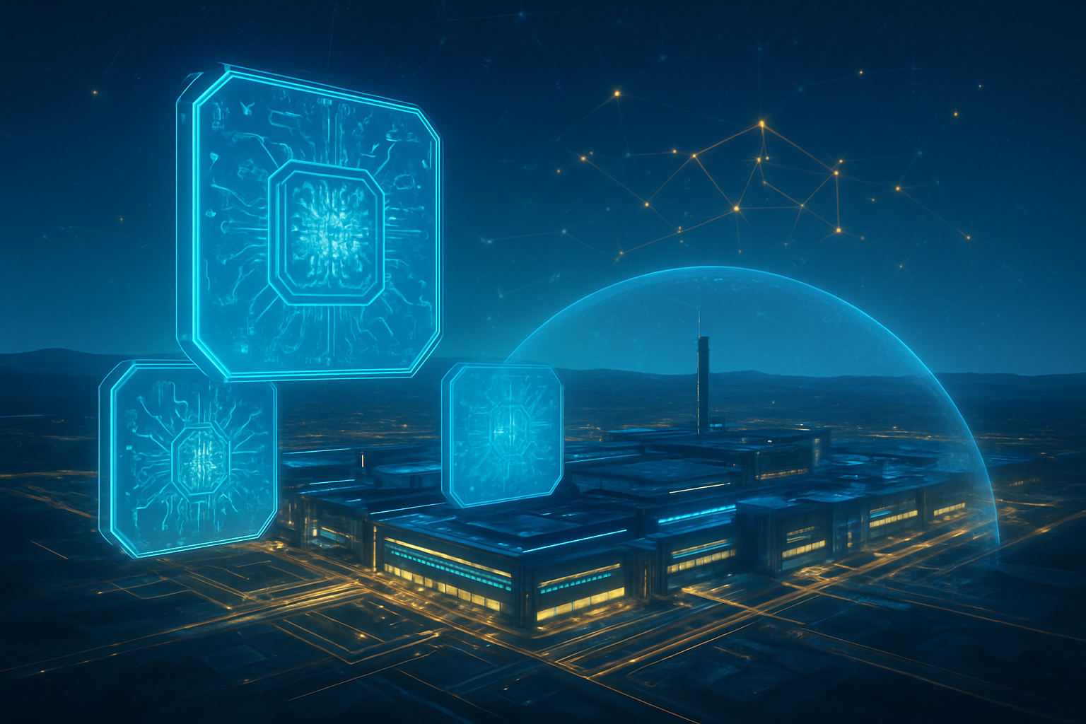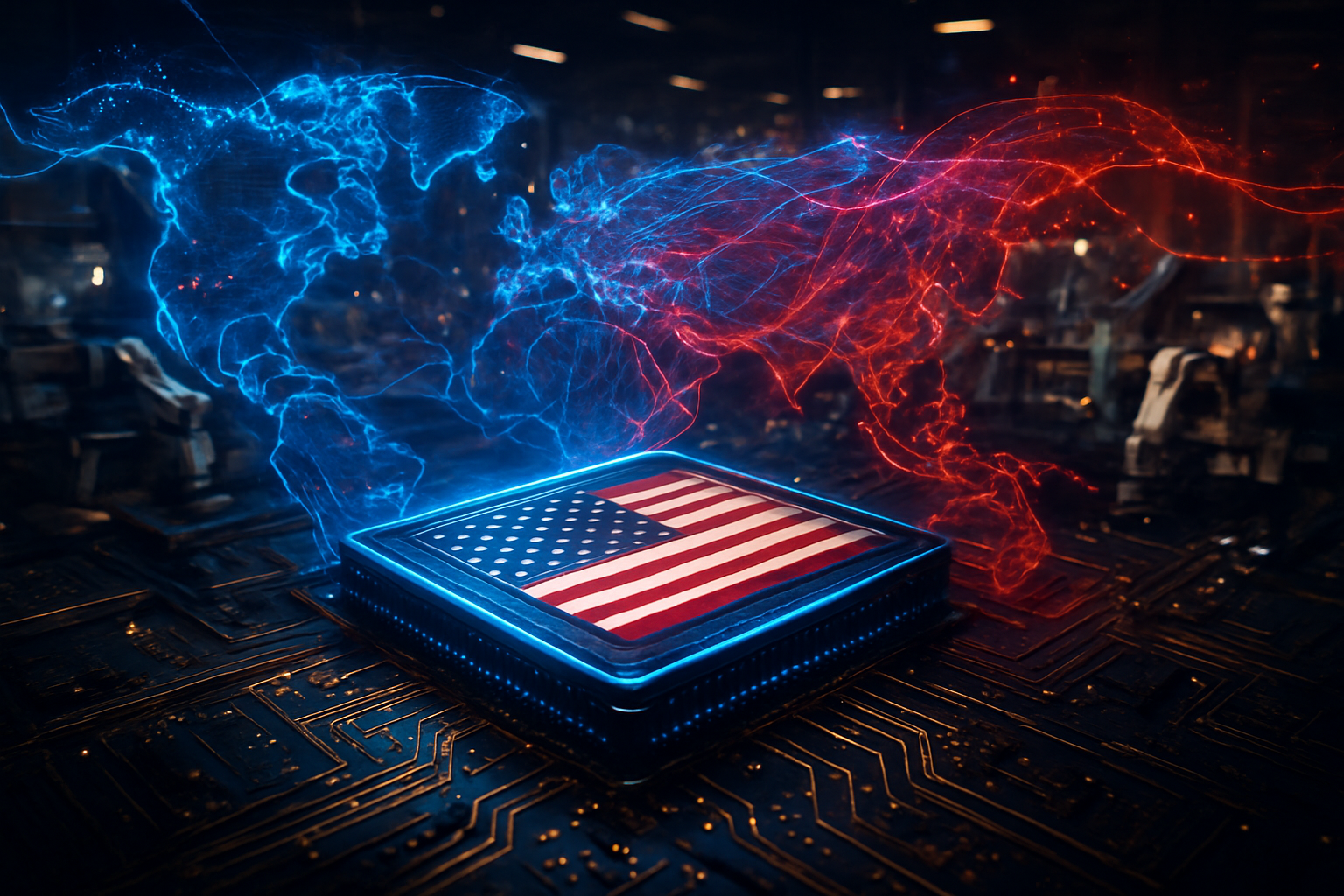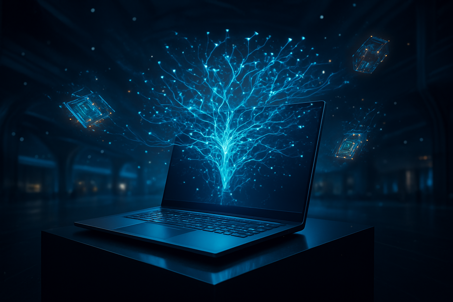
The tech industry has officially crossed the Rubicon. Following the conclusion of CES 2026 in Las Vegas, the narrative surrounding artificial intelligence has shifted from experimental cloud-based chatbots to "Silicon Sovereignty"—the ability for personal devices to execute complex, multi-step "Agentic AI" tasks without ever sending data to a remote server. This transition marks the end of the AI prototype era and the beginning of large-scale, edge-native deployment, where the operating system itself is no longer just a file manager, but a proactive digital agent.
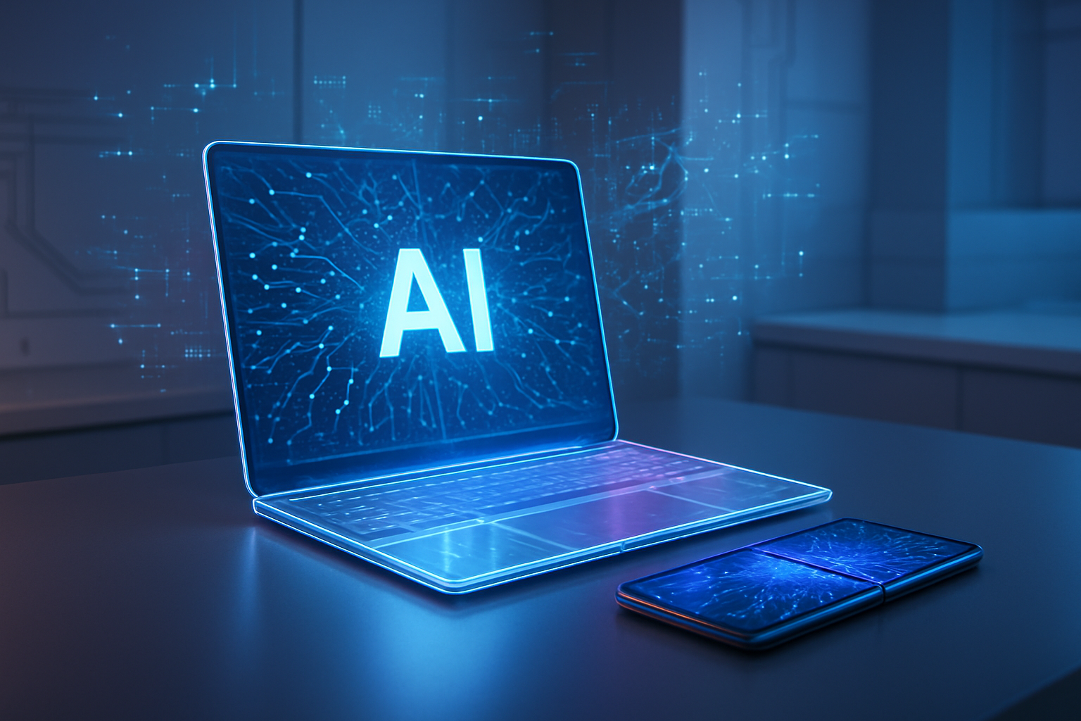
The significance of this shift cannot be overstated. For the past two years, AI was largely something you visited via a browser or a specialized app. As of January 2026, AI is something your hardware is. With the introduction of standardized Neural Processing Units (NPUs) delivering upwards of 50 to 80 TOPS (Trillion Operations Per Second), the "AI PC" and the "AI-native smartphone" have moved from marketing buzzwords to essential hardware requirements for the modern workforce and consumer.
The 50 TOPS Threshold: A New Baseline for Local Intelligence
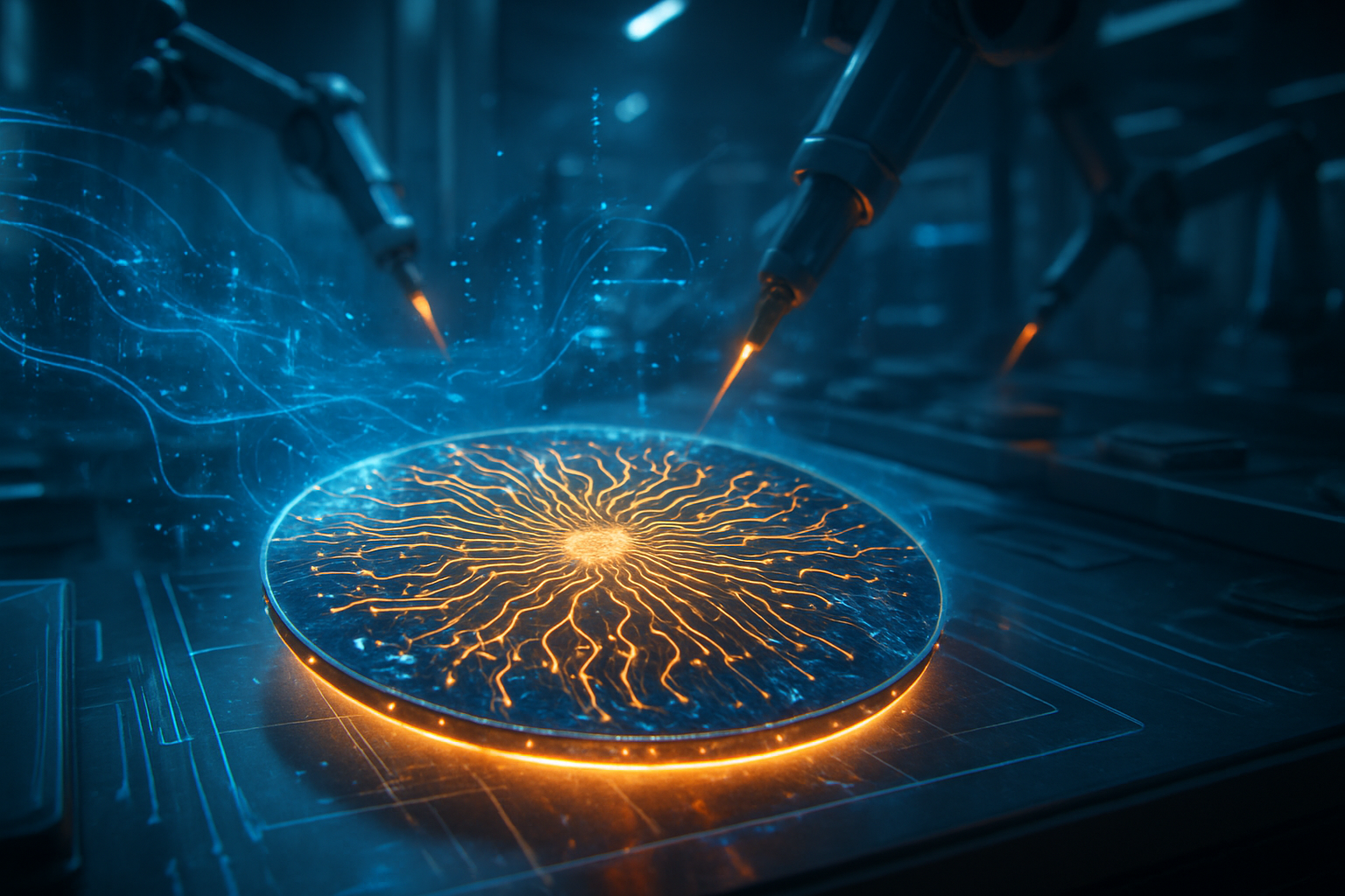
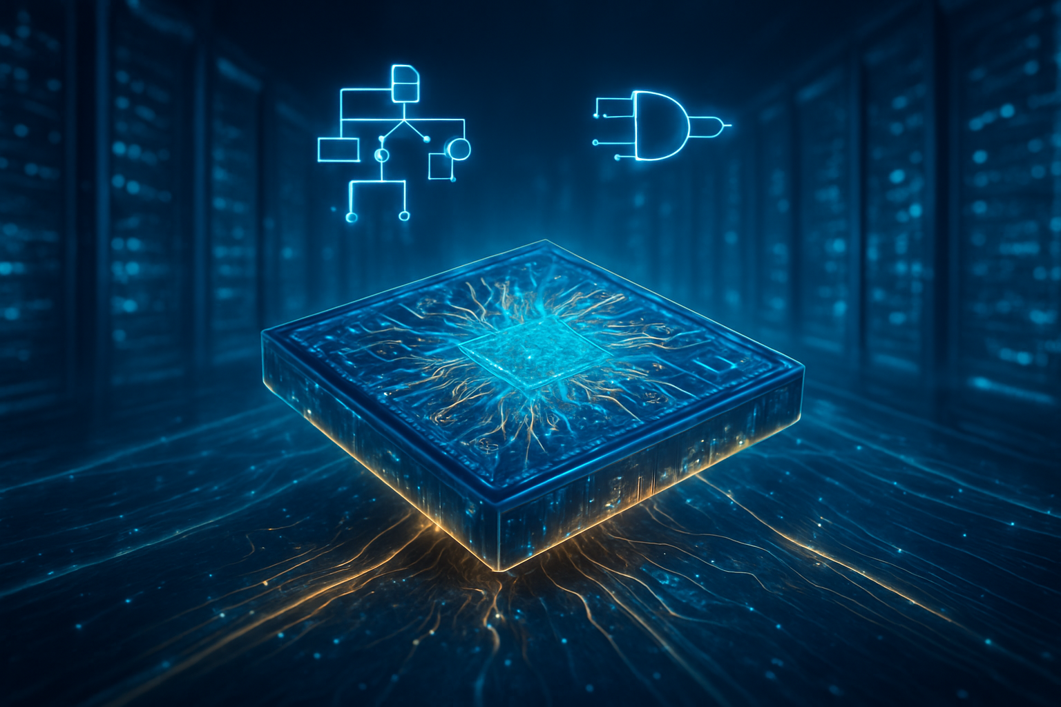
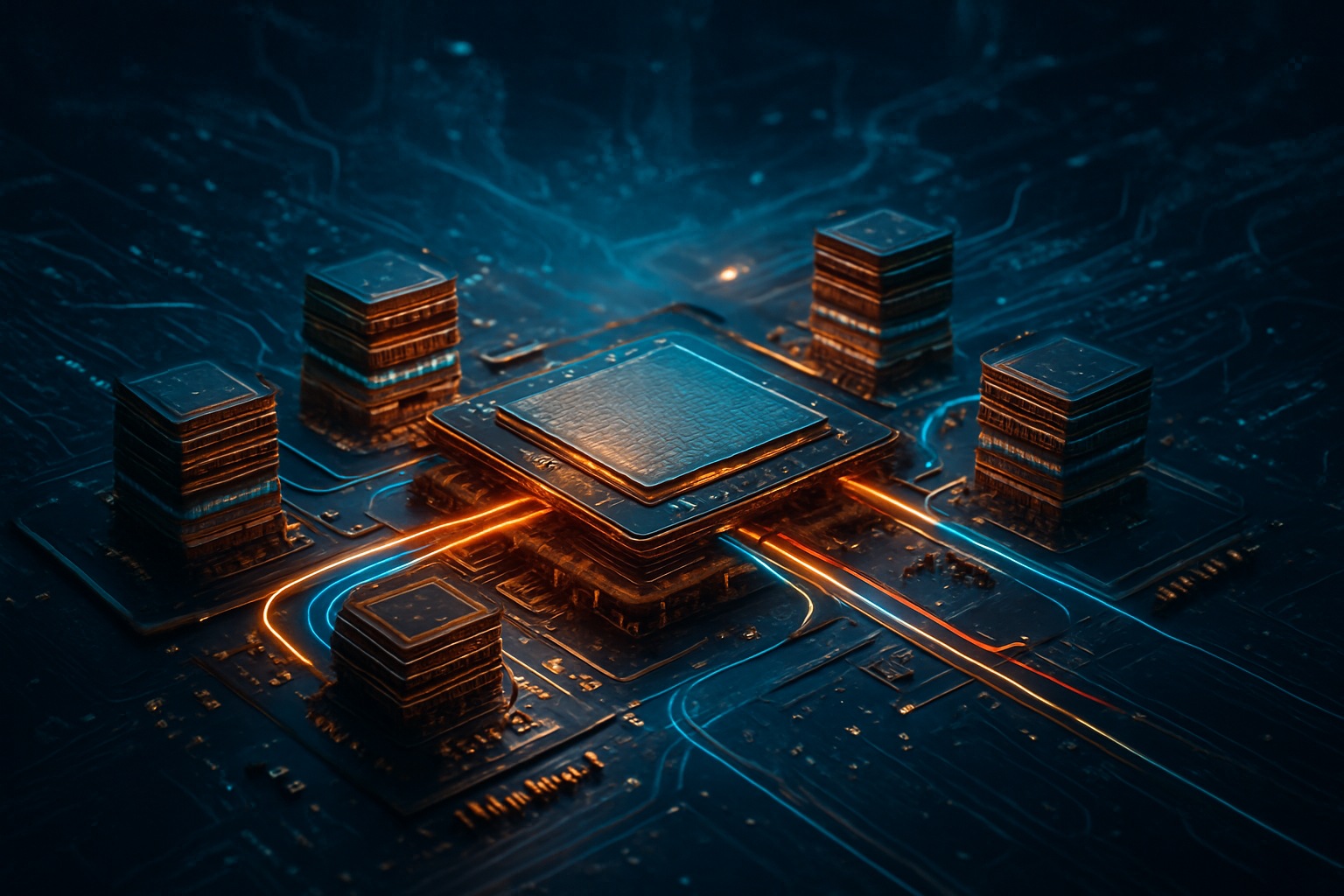
At the heart of this revolution is a massive leap in specialized silicon. Intel (NASDAQ: INTC) dominated the CES stage with the official launch of its Core Ultra Series 3 processors, codenamed "Panther Lake." Built on the cutting-edge Intel 18A process node, these chips feature the NPU 5, which delivers a dedicated 50 TOPS. When combined with the integrated Arc B390 graphics, the platform's total AI throughput reaches a staggering 180 TOPS. This allows for the local execution of large language models (LLMs) with billions of parameters, such as a specialized version of Mistral or Meta’s (NASDAQ: META) Llama 4-mini, with near-zero latency.
AMD (NASDAQ: AMD) countered with its Ryzen AI 400 Series, "Gorgon Point," which pushes the NPU envelope even further to 60 TOPS using its second-generation XDNA 2 architecture. Not to be outdone in the mobile and efficiency space, Qualcomm (NASDAQ: QCOM) unveiled the Snapdragon X2 Plus for PCs and the Snapdragon 8 Elite Gen 5 for smartphones. The X2 Plus sets a new efficiency record with 80 NPU TOPS, specifically optimized for "Local Fine-Tuning," a feature that allows the device to learn a user’s writing style and preferences entirely on-device. Meanwhile, NVIDIA (NASDAQ: NVDA) reinforced its dominance in the high-end enthusiast market with the GeForce RTX 50 Series "Blackwell" laptop GPUs, providing over 3,300 TOPS for local model training and professional generative workflows.
The technical community has noted that this shift differs fundamentally from the "AI-enhanced" laptops of 2024. Those earlier devices primarily used NPUs for simple tasks like background blur in video calls. The 2026 generation uses the NPU as the primary engine for "Agentic AI"—systems that can autonomously manage files, draft complex responses based on local context, and orchestrate workflows across different applications. Industry experts are calling this the "death of the NPU idle state," as these units are now consistently active, powering a persistent "AI Shell" that sits between the user and the operating system.
The Disruption of the Subscription Model and the Rise of the Edge
This hardware surge is sending shockwaves through the business models of the world’s leading AI labs. For the last several years, the $20-per-month subscription model for premium chatbots was the industry standard. However, the emergence of powerful local hardware is making these subscriptions harder to justify for the average user. At CES 2026, Samsung (KRX: 005930) and Lenovo (HKG: 0992) both announced that their core "Agentic" features would be bundled with the hardware at no additional cost. When your laptop can summarize a 100-page PDF or edit a video via voice command locally, the need for a cloud-based GPT or Claude subscription diminishes.
Cloud hyperscalers like Microsoft (NASDAQ: MSFT), Alphabet (NASDAQ: GOOGL), and Amazon (NASDAQ: AMZN) are being forced to pivot. While their cloud infrastructure remains vital for training massive models like GPT-5.2 or Claude 4, they are seeing a "hollowing out" of low-complexity inference revenue. Microsoft’s response, the "Windows AI Foundry," effectively standardizes how Windows 12 offloads tasks between local NPUs and the Azure cloud. This creates a hybrid model where the cloud is reserved only for "heavy reasoning" tasks that exceed the local 50-80 TOPS threshold.
Smaller, more agile AI startups are finding new life in this edge-native world. Mistral has repositioned itself as the "on-device default," partnering with Qualcomm and Intel to optimize its "Ministral" models for specific NPU architectures. Similarly, Perplexity is moving from being a standalone search engine to the "world knowledge layer" for local agents like Lenovo’s new "Qira" assistant. In this new landscape, the strategic advantage has shifted from who has the largest server farm to who has the most efficient model that can fit into a smartphone's thermal envelope.
Privacy, Personal Knowledge Graphs, and the Broader AI Landscape
The move to local AI is also a response to growing consumer anxiety over data privacy. A central theme at CES 2026 was the "Personal Knowledge Graph" (PKG). Unlike cloud AI, which sees only what you type into a chat box, these new AI-native devices index everything—emails, calendar invites, local files, and even screen activity—to create a "perfect context" for the user. While this enables a level of helpfulness never before seen, it also creates significant security concerns.
Privacy advocates at the show raised alarms about "Privilege Escalation" and "Metadata Leaks." If a local agent has access to your entire financial history to help you with taxes, a malicious prompt or a security flaw could theoretically allow that data to be exported. To mitigate this, manufacturers are implementing hardware-isolated vaults, such as Samsung’s "Knox Matrix," which requires biometric authentication before an AI agent can access sensitive parts of the PKG. This "Trust-by-Design" architecture is becoming a major selling point for enterprise buyers who are wary of cloud-based data leaks.
This development fits into a broader trend of "de-centralization" in AI. Just as the PC liberated computing from the mainframe in the 1980s, the AI PC is liberating intelligence from the data center. However, this shift is not without its challenges. The EU AI Act, now fully in effect, and new California privacy amendments are forcing companies to include "Emergency Kill Switches" for local agents. The landscape is becoming a complex map of high-performance silicon, local privacy vaults, and stringent regulatory oversight.
The Future: From Apps to Agents
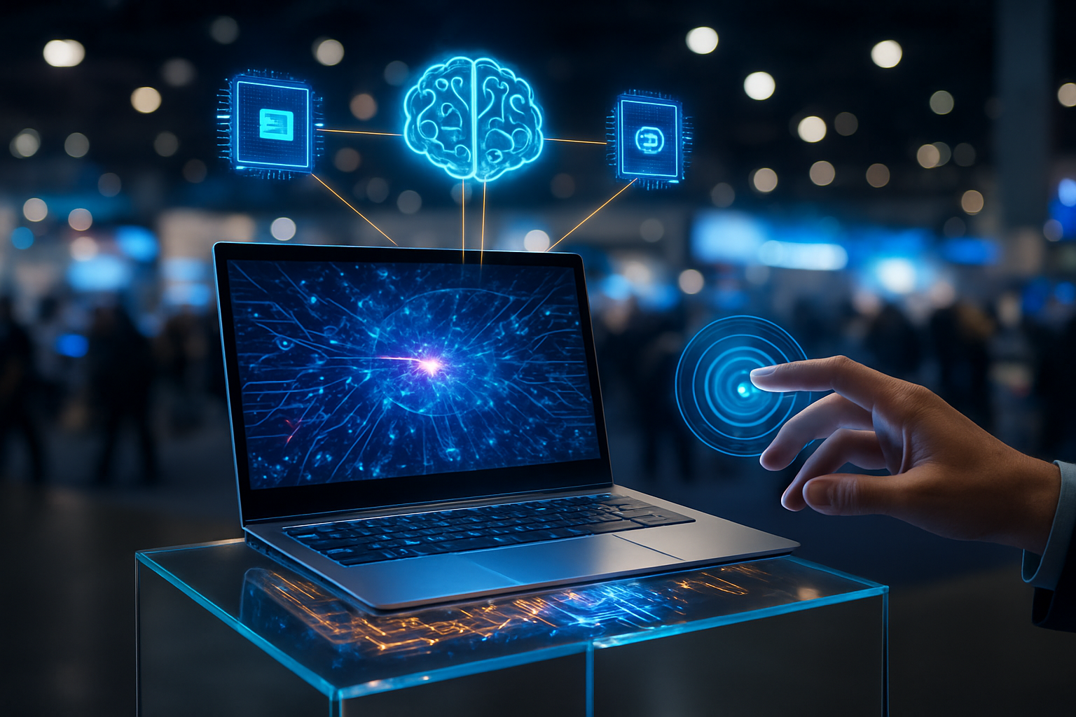
Looking toward the latter half of 2026 and into 2027, experts predict the total disappearance of the "app" as we know it. We are entering the "Post-App Era," where users interact with a single agentic interface that pulls functionality from various services in the background. Instead of opening a travel app, a banking app, and a calendar app to book a trip, a user will simply tell their AI-native phone to "Organize my trip to Tokyo," and the local agent will coordinate the entire process using its access to the user's PKG and secure payment tokens.
The next frontier will be "Ambient Intelligence"—the ability for your AI agents to follow you seamlessly from your phone to your PC to your smart car. Lenovo’s "Qira" system already demonstrates this, allowing a user to start a task on a Motorola smartphone and finish it on a ThinkPad with full contextual continuity. The challenge remaining is interoperability; currently, Samsung’s agents don’t talk to Apple’s (NASDAQ: AAPL) agents, creating new digital silos that may require industry-wide standards to resolve.
A New Chapter in Computing History
The emergence of AI PCs and AI-native smartphones at CES 2026 will likely be remembered as the moment AI became invisible. Much like the transition from dial-up to broadband, the shift from cloud-laggy chatbots to instantaneous, local agentic intelligence changes the fundamental way we interact with technology. The hardware is finally catching up to the software’s promises, and the 50 TOPS NPU is the engine of this change.
As we move forward into 2026, the tech industry will be watching the adoption rates of these new devices closely. With the "Windows AI Foundry" and new Android AI shells becoming the standard, the pressure is now on developers to build "Agentic-first" software. For consumers, the message is clear: the most powerful AI in the world is no longer in a distant data center—it’s in your pocket and on your desk.
This content is intended for informational purposes only and represents analysis of current AI developments.
TokenRing AI delivers enterprise-grade solutions for multi-agent AI workflow orchestration, AI-powered development tools, and seamless remote collaboration platforms.
For more information, visit https://www.tokenring.ai/.