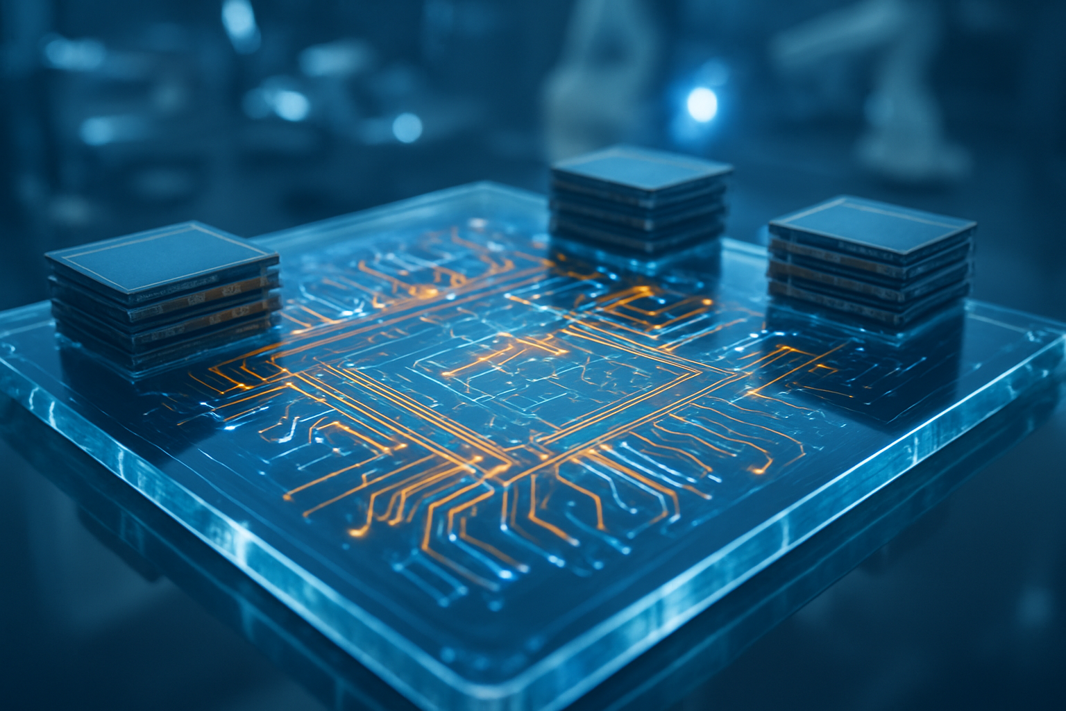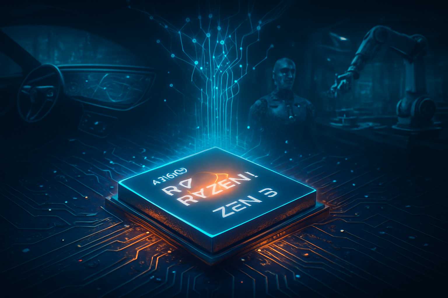
LAS VEGAS — At the 2026 Consumer Electronics Show (CES), Advanced Micro Devices (NASDAQ: AMD) officially signaled its intent to dominate the rapidly expanding edge AI market. The company announced the launch of the Ryzen AI Embedded P100 and X100 series, a groundbreaking family of processors designed to bring high-performance "Physical AI" to the industrial and automotive sectors. By integrating the latest Zen 5 CPU architecture with a dedicated XDNA 2 Neural Processing Unit (NPU), AMD is positioning itself as the primary architect for the intelligent machines of the future, from humanoid robots to fully digital vehicle cockpits.
The announcement marks a pivotal shift in the embedded computing landscape. Historically, high-level AI inference was relegated to power-hungry discrete GPUs or remote cloud servers. With the P100 and X100 series, AMD (NASDAQ: AMD) delivers up to 50 TOPS (Trillions of Operations Per Second) of dedicated AI performance in a power-efficient, single-chip solution. This development is expected to accelerate the deployment of autonomous systems that require immediate, low-latency decision-making without the privacy risks or connectivity dependencies of the cloud.
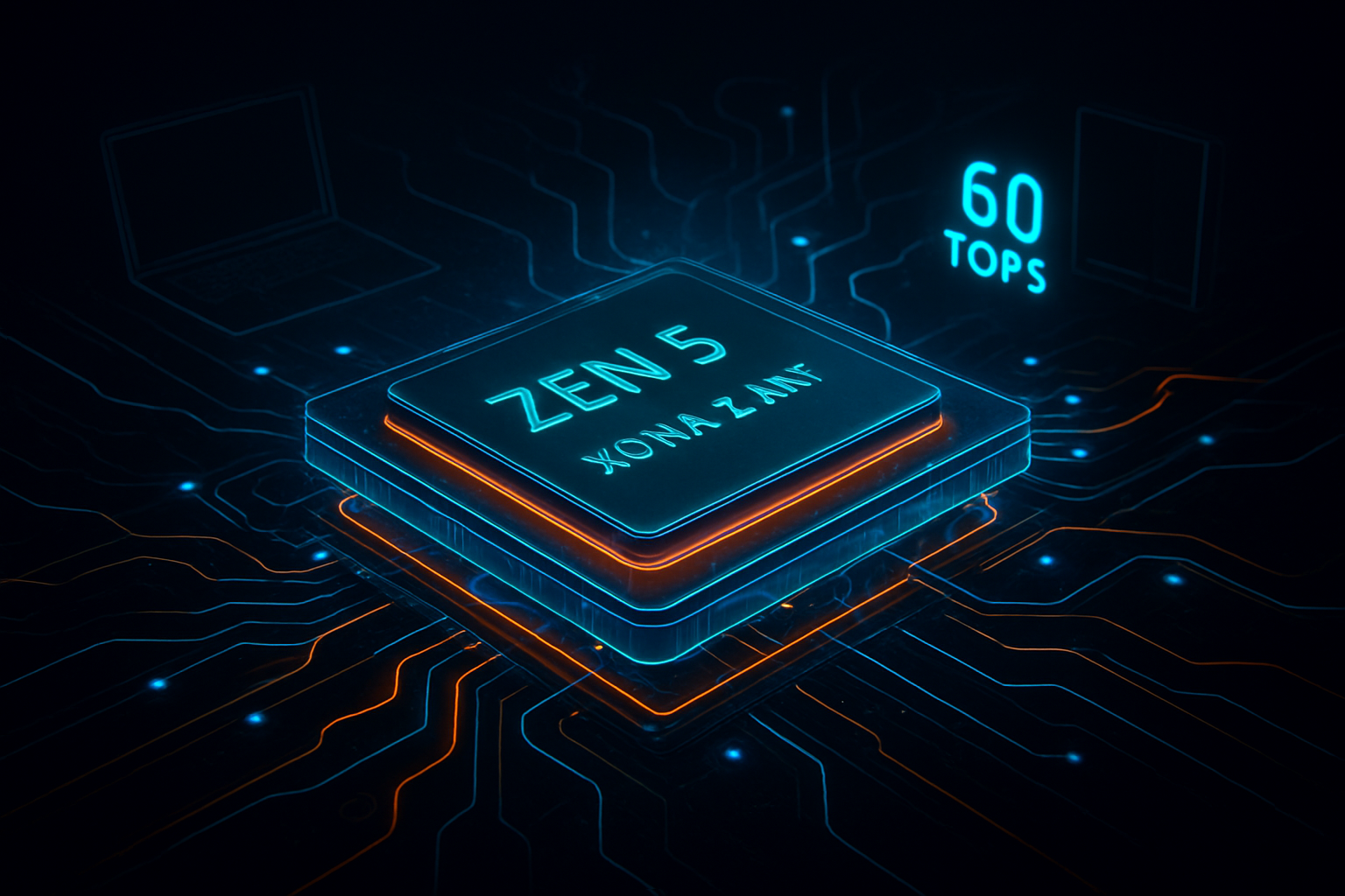
Technical Prowess: Zen 5 and the 50 TOPS Threshold
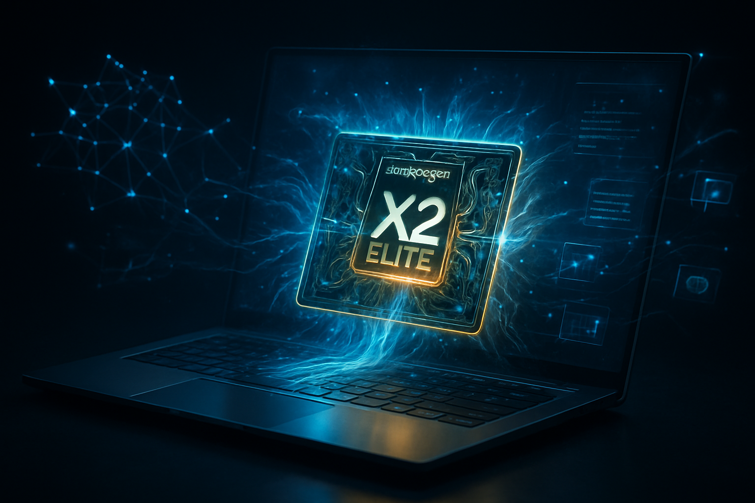
The Ryzen AI Embedded P100 and X100 series are built on a cutting-edge 4nm process, utilizing a hybrid architecture of "Zen 5" high-performance cores and "Zen 5c" efficiency cores. This combination allows the processors to handle complex multi-threaded workloads—such as running a vehicle's infotainment system while simultaneously monitoring driver fatigue—with a 2.2X performance-per-watt improvement over the previous Ryzen Embedded 8000 generation. The flagship X100 series scales up to 16 cores, providing the raw computational horsepower needed for the most demanding "Physical AI" applications.
The true centerpiece of this new silicon is the XDNA 2 NPU. Delivering a massive 3x jump in AI throughput compared to its predecessor, the XDNA 2 architecture is optimized for vision transformers and compact Large Language Models (LLMs). For the first time, embedded developers can run sophisticated generative AI models locally on the device. Complementing the AI engine is the RDNA 3.5 graphics architecture, which supports up to four simultaneous 4K displays. This makes the P100 series a formidable choice for automotive digital cockpits, where high-fidelity 3D maps and augmented reality overlays must be rendered in real-time with zero lag.
Initial reactions from the industrial research community have been overwhelmingly positive. Experts note that the inclusion of Time-Sensitive Networking (TSN) and ECC memory support makes these chips uniquely suited for "deterministic" AI—where timing is critical. Unlike consumer-grade chips, the P100/X100 series are AEC-Q100 qualified, meaning they can operate in the extreme temperature ranges (-40°C to +105°C) required for automotive and heavy industrial environments.
Shifting the Competitive Landscape: AMD vs. NVIDIA and Intel
This move places AMD in direct competition with NVIDIA (NASDAQ: NVDA) and its dominant Jetson platform. While NVIDIA has long held the lead in edge AI through its CUDA ecosystem, AMD is countering with an "open-source first" strategy. By leveraging the ROCm 7 software stack and the unified Ryzen AI software flow, AMD allows developers to port AI models seamlessly from EPYC-powered cloud servers to Ryzen-powered edge devices. This interoperability could disrupt the market for startups and OEMs who are wary of the "vendor lock-in" associated with proprietary AI platforms.
Intel (NASDAQ: INTC) also finds itself in a tightening race. While Intel’s Core Ultra "Panther Lake" embedded chips offer competitive AI features, AMD’s integration of the XDNA 2 NPU currently leads in raw TOPS-per-watt for the embedded sector. Market analysts suggest that AMD’s aggressive 10-year production lifecycle guarantee for the P100/X100 series will be a major selling point for industrial giants like Siemens and Bosch, who require long-term hardware stability for factory automation lines that may remain in service for over a decade.
For the automotive sector, the P100 series targets the "multi-domain" architecture trend. Rather than having separate chips for the dashboard, navigation, and driver assistance, car manufacturers can now consolidate these functions into a single AMD-powered module. This consolidation reduces vehicle weight, lowers power consumption, and simplifies the complex software supply chain for next-generation electric vehicles (EVs).
The Rise of Physical AI and the Local Processing Revolution
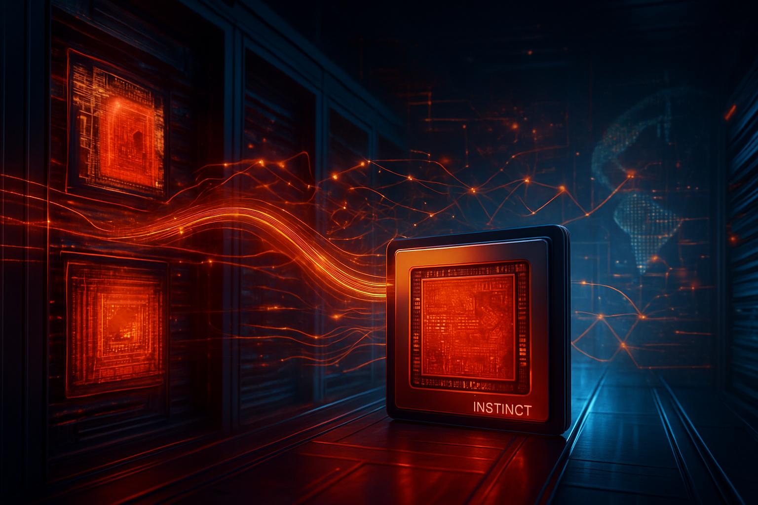
The launch of the X100 series specifically targets the nascent field of humanoid robotics. As companies like Tesla (NASDAQ: TSLA) and Figure AI race to bring general-purpose robots to factory floors, the need for "on-robot" intelligence has become paramount. A humanoid robot must process vast amounts of visual and tactile data in milliseconds to navigate a dynamic environment. By providing 50 TOPS of local NPU performance, AMD enables these machines to interpret natural language commands and recognize objects without sending data to a central server, ensuring both speed and data privacy.
This transition from cloud-centric AI to "Edge AI" is a defining trend of 2026. As AI models become more efficient through techniques like quantization, the hardware's ability to execute these models locally becomes the primary bottleneck. AMD’s expansion reflects a broader industry realization: for AI to be truly ubiquitous, it must be invisible, reliable, and decoupled from the internet. This "Local AI" movement addresses growing societal concerns regarding data harvesting and the vulnerability of critical infrastructure to network outages.
Furthermore, the environmental impact of this shift cannot be understated. By moving inference from massive, water-cooled data centers to efficient edge chips, the carbon footprint of AI operations is significantly reduced. AMD’s focus on the Zen 5c efficiency cores demonstrates a commitment to sustainable computing that resonates with ESG-conscious corporate buyers in the industrial sector.
Looking Ahead: The Future of Autonomous Systems
In the near term, expect to see the first wave of P100-powered vehicles and industrial controllers hit the market by mid-2026. Early adopters are likely to be in the high-end EV space and advanced logistics warehouses. However, the long-term potential lies in the democratization of sophisticated robotics. As the cost of high-performance AI silicon drops, we may see the X100 series powering everything from autonomous delivery drones to robotic surgical assistants.
Challenges remain, particularly in the software ecosystem. While ROCm 7 is a significant step forward, NVIDIA still holds a massive lead in developer mindshare. AMD will need to continue its aggressive outreach to the AI research community to ensure that the latest models are optimized for XDNA 2 out of the box. Additionally, as AI becomes more integrated into physical safety systems, regulatory scrutiny over "deterministic AI" performance will likely increase, requiring AMD to work closely with safety certification bodies.
A New Chapter for Embedded AI
The introduction of the Ryzen AI Embedded P100 and X100 series is more than just a hardware refresh; it is a declaration of AMD's (NASDAQ: AMD) vision for the next decade of computing. By bringing the power of Zen 5 and XDNA 2 to the edge, AMD is providing the foundational "brains" for a new generation of autonomous, intelligent, and efficient machines.
The significance of this development in AI history lies in its focus on "Physical AI"—the bridge between digital intelligence and the material world. As we move through 2026, the success of these chips will be measured not just by benchmarks, but by the autonomy of the robots they power and the safety of the vehicles they control. Investors and tech enthusiasts should keep a close eye on AMD’s upcoming partnership announcements with major automotive and robotics firms in the coming months, as these will signal the true scale of AMD's edge AI ambitions.
This content is intended for informational purposes only and represents analysis of current AI developments.
TokenRing AI delivers enterprise-grade solutions for multi-agent AI workflow orchestration, AI-powered development tools, and seamless remote collaboration platforms.
For more information, visit https://www.tokenring.ai/.