In a move that has sent shockwaves through the global technology sector, Advanced Micro Devices (NASDAQ: AMD) and OpenAI have finalized a strategic partnership that fundamentally redefines the artificial intelligence hardware landscape. The deal, announced in late 2025, centers on a massive deployment of AMD’s next-generation MI450 accelerators within a dedicated 1-gigawatt (GW) data center facility. This unprecedented infrastructure project is not merely a supply agreement; it includes a transformative equity arrangement granting OpenAI a warrant to acquire up to 160 million shares of AMD common stock—effectively a 10% ownership stake in the chipmaker—tied to the successful rollout of the new hardware.
This partnership represents the most significant challenge to the long-standing dominance of NVIDIA (NASDAQ: NVDA) in the AI compute market. By securing a massive, guaranteed supply of high-performance silicon and a direct financial interest in the success of its primary hardware vendor, OpenAI is insulating itself against the supply chain bottlenecks and premium pricing that have characterized the H100 and Blackwell eras. For AMD, the deal provides a massive $30 billion revenue infusion for the initial phase alone, cementing its status as a top-tier provider of the foundational infrastructure required for the next generation of artificial general intelligence (AGI) models.
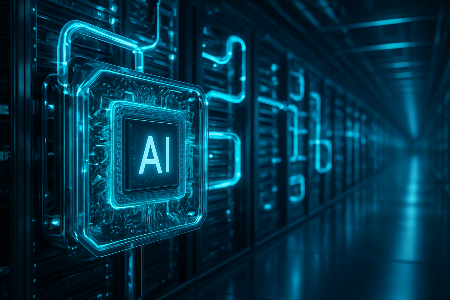
The MI450 Breakthrough: A New Era of Compute Density
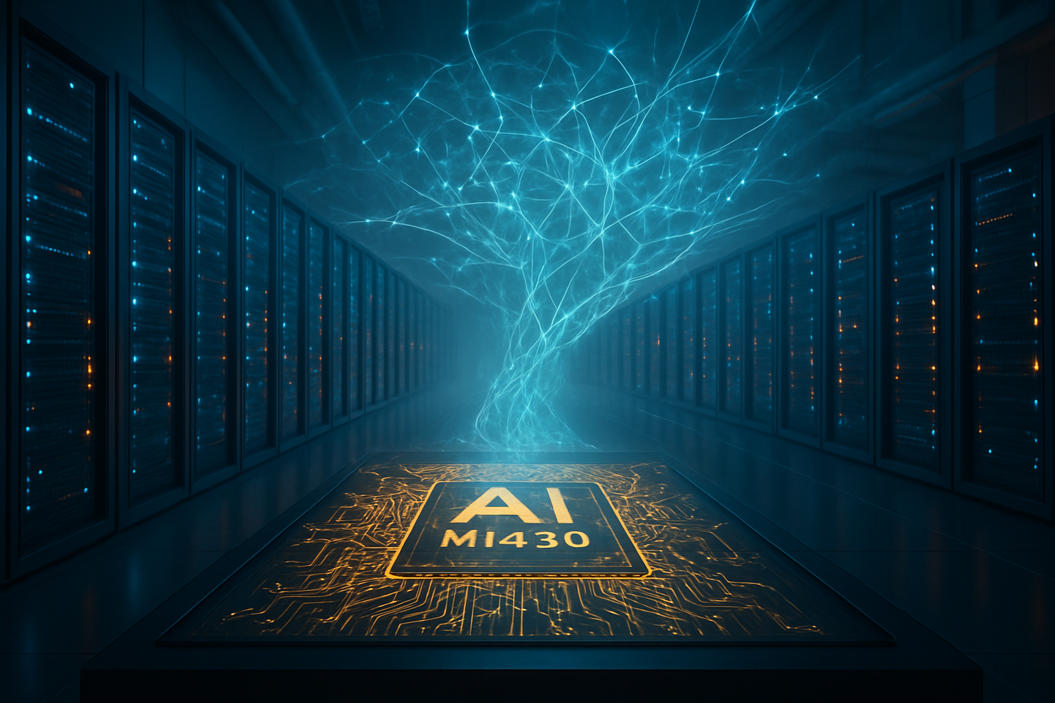
The technical cornerstone of this alliance is the AMD Instinct MI450, a chip that industry analysts are calling AMD’s "Milan moment" for the AI era. Built on a cutting-edge 3nm-class process using advanced CoWoS-L packaging, the MI450 is designed specifically to handle the massive parameter counts of OpenAI's upcoming models. Each GPU boasts an unprecedented memory capacity ranging from 288 GB to 432 GB of HBM4 memory, delivering a staggering 18 TB/s of sustained bandwidth. This allows for the training of models that were previously memory-bound, significantly reducing the overhead of data movement across clusters.
In terms of raw compute, the MI450 delivers approximately 50 PetaFLOPS of FP4 performance per card, placing it in direct competition with NVIDIA’s Rubin architecture. To support this density, AMD has introduced the Helios rack-scale system, which clusters 128 GPUs into a single logical unit using the new UALink connectivity and an Ethernet-based Infinity Fabric. This "IF128" configuration provides 6,400 PetaFLOPS of compute per rack, though it comes with a significant power requirement, with each individual GPU drawing between 1.6 kW and 2.0 kW.
Initial reactions from the AI research community have been overwhelmingly positive, particularly regarding AMD’s commitment to open software ecosystems. While NVIDIA’s CUDA has long been the industry standard, OpenAI has been a primary driver of the Triton programming language, which allows for high-performance kernel development across different hardware backends. The tight integration between OpenAI’s software stack and AMD’s ROCm platform on the MI450 suggests that the "CUDA moat" may finally be narrowing, as developers find it increasingly easy to port state-of-the-art models to AMD hardware without performance penalties.
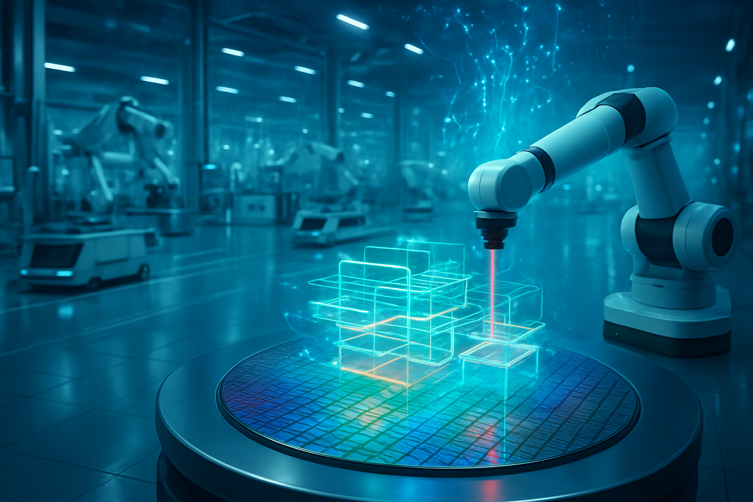
The 1-gigawatt facility itself, located in Abilene, Texas, as part of the broader "Project Stargate" initiative, is a marvel of modern engineering. This facility is the first of its kind to be designed from the ground up for liquid-cooled, high-density AI clusters at this scale. By dedicating the entire 1 GW capacity to the MI450 rollout, OpenAI is creating a homogeneous environment that simplifies orchestration and maximizes the efficiency of its training runs. The facility is expected to be fully operational by the second half of 2026, marking a new milestone in the physical scale of AI infrastructure.
Market Disruption and the End of the GPU Monoculture
The strategic implications for the tech industry are profound, as this deal effectively ends the "GPU monoculture" that has favored NVIDIA for the past three years. By diversifying its hardware providers, OpenAI is not only reducing its operational risks but also gaining significant leverage in future negotiations. Other major AI labs, such as Anthropic and Google (NASDAQ: GOOGL), are likely to take note of this successful pivot, potentially leading to a broader industry shift toward AMD and custom silicon solutions.
NVIDIA, while still the market leader, now faces a competitor that is backed by the most influential AI company in the world. The competitive landscape is shifting from a battle of individual chips to a battle of entire ecosystems and supply chains. Microsoft (NASDAQ: MSFT), which remains OpenAI’s primary cloud partner, is also a major beneficiary, as it will host a significant portion of this AMD-powered infrastructure within its Azure cloud, further diversifying its own hardware offerings and reducing its reliance on a single vendor.
Furthermore, the 10% stake option for OpenAI creates a unique "vendor-partner" hybrid model that could become a blueprint for future tech alliances. This alignment of interests ensures that AMD’s product roadmap will be heavily influenced by OpenAI’s specific needs for years to come. For startups and smaller AI companies, this development is a double-edged sword: while it may lead to more competitive pricing for AI compute in the long run, it also risks a scenario where the most advanced hardware is locked behind exclusive partnerships between the largest players in the industry.
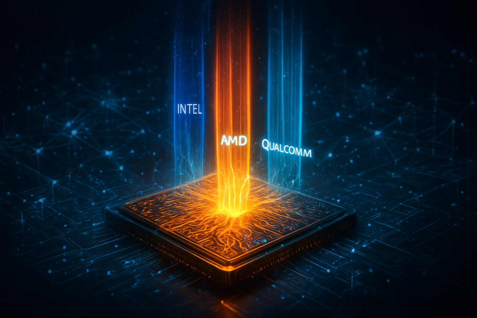
The financial markets have reacted with cautious optimism for AMD, seeing the deal as a validation of their long-term AI strategy. While the dilution from OpenAI’s potential 160 million shares is a factor for current shareholders, the guaranteed $100 billion in projected revenue over the next four years is a powerful counter-argument. The deal also places pressure on other chipmakers like Intel (NASDAQ: INTC) to prove their relevance in the high-end AI accelerator market, which is increasingly being dominated by a duopoly of NVIDIA and AMD.
Energy, Sovereignty, and the Global AI Landscape
On a broader scale, the 1-gigawatt facility highlights the escalating energy demands of the AI revolution. The sheer scale of the Abilene site—equivalent to the power output of a large nuclear reactor—underscores the fact that AI progress is now as much a challenge of energy production and distribution as it is of silicon design. This has sparked renewed discussions about "AI Sovereignty," as nations and corporations scramble to secure the massive amounts of power and land required to host these digital titans.
This milestone is being compared to the early days of the Manhattan Project or the Apollo program in terms of its logistical and financial scale. The move toward 1 GW sites suggests that the era of "modest" data centers is over, replaced by a new paradigm of industrial-scale AI campuses. This shift brings with it significant environmental and regulatory concerns, as local grids struggle to adapt to the massive, constant loads required by MI450 clusters. OpenAI and AMD have addressed this by committing to carbon-neutral power sources for the Texas site, though the long-term sustainability of such massive power consumption remains a point of intense debate.
The partnership also reflects a growing trend of vertical integration in the AI industry. By taking an equity stake in its hardware provider and co-designing the data center architecture, OpenAI is moving closer to the model pioneered by Apple (NASDAQ: AAPL), where hardware and software are developed in tandem for maximum efficiency. This level of integration is seen as a prerequisite for achieving the next major breakthroughs in model reasoning and autonomy, as the hardware must be perfectly tuned to the specific architectural quirks of the neural networks it runs.
However, the deal is not without its critics. Some industry observers have raised concerns about the concentration of power in a few hands, noting that an OpenAI-AMD-Microsoft triad could exert undue influence over the future of AI development. There are also questions about the "performance-based" nature of the equity warrant, which could incentivize AMD to prioritize OpenAI’s needs at the expense of its other customers. Comparisons to previous milestones, such as the initial launch of the DGX-1 or the first TPU, suggest that while those were technological breakthroughs, the AMD-OpenAI deal is a structural breakthrough for the entire industry.
The Horizon: From MI450 to AGI
Looking ahead, the roadmap for the AMD-OpenAI partnership extends far beyond the initial 1 GW rollout. Plans are already in place for the MI500 series, which is expected to debut in 2027 and will likely feature even more advanced 2nm processes and integrated optical interconnects. The goal is to scale the total deployed capacity to 6 GW by 2029, a scale that was unthinkable just a few years ago. This trajectory suggests that OpenAI is betting its entire future on the belief that more compute will continue to yield more capable and intelligent systems.
Potential applications for this massive compute pool include the development of "World Models" that can simulate physical reality with high fidelity, as well as the training of autonomous agents capable of long-term planning and scientific discovery. The challenges remain significant, particularly in the realm of software orchestration at this scale and the mitigation of hardware failures in clusters containing hundreds of thousands of GPUs. Experts predict that the next two years will be a period of intense experimentation as OpenAI learns how to best utilize this unprecedented level of heterogeneous compute.
As the first tranche of the equity warrant vests upon the completion of the Abilene facility, the industry will be watching closely to see if the MI450 can truly match the reliability and software maturity of NVIDIA’s offerings. If successful, this partnership will be remembered as the moment the AI industry matured from a wild-west scramble for chips into a highly organized, vertically integrated industrial sector. The race to AGI is now a race of gigawatts and equity stakes, and the AMD-OpenAI alliance has just set a new pace.
Conclusion: A New Foundation for the Future of AI
The partnership between AMD and OpenAI is more than just a business deal; it is a foundational shift in the hierarchy of the technology world. By combining AMD’s increasingly competitive silicon with OpenAI’s massive compute requirements and software expertise, the two companies have created a formidable alternative to the status quo. The 1-gigawatt facility in Texas stands as a physical monument to this ambition, representing a scale of investment and technical complexity that few other entities on Earth can match.
Key takeaways from this development include the successful diversification of the AI hardware supply chain, the emergence of the MI450 as a top-tier accelerator, and the innovative use of equity to align the interests of hardware and software giants. As we move into 2026, the success of this alliance will be measured not just in stock prices or benchmarks, but in the capabilities of the AI models that emerge from the Abilene super-facility. This is a defining moment in the history of artificial intelligence, signaling the transition to an era of industrial-scale compute.
In the coming months, the industry will be focused on the first "power-on" tests in Texas and the subsequent software optimization reports from OpenAI’s engineering teams. If the MI450 performs as promised, the ripple effects will be felt across every corner of the tech economy, from energy providers to cloud competitors. For now, the message is clear: the path to the future of AI is being paved with AMD silicon, powered by gigawatts of energy, and secured by a historic 10% stake in the future of computing.
This content is intended for informational purposes only and represents analysis of current AI developments.
TokenRing AI delivers enterprise-grade solutions for multi-agent AI workflow orchestration, AI-powered development tools, and seamless remote collaboration platforms.
For more information, visit https://www.tokenring.ai/.