Advanced Micro Devices (NASDAQ:AMD) is mounting its most formidable challenge yet to NVIDIA’s (NASDAQ:NVDA) long-standing dominance in the AI hardware market. With the official launch of the Instinct MI350 series, featuring the flagship MI355X, AMD has introduced a powerhouse accelerator that finally achieves performance parity—and in some cases, superiority—over NVIDIA’s Blackwell B200 architecture. This release marks a pivotal shift in the AI industry, signaling that the "CUDA moat" is no longer the impenetrable barrier it once was for the world's largest AI developers.
The significance of the MI350 series lies not just in its raw compute power, but in its strategic focus on memory capacity and cost efficiency. As of late 2025, the demand for inference—running already-trained AI models—has overtaken the demand for training, and AMD has optimized the MI350 series specifically for this high-growth sector. By offering 288GB of high-bandwidth memory (HBM3E) per chip, AMD is enabling enterprises to run the world's largest models, such as Llama 4 and GPT-5, on fewer nodes, significantly reducing the total cost of ownership for data center operators.
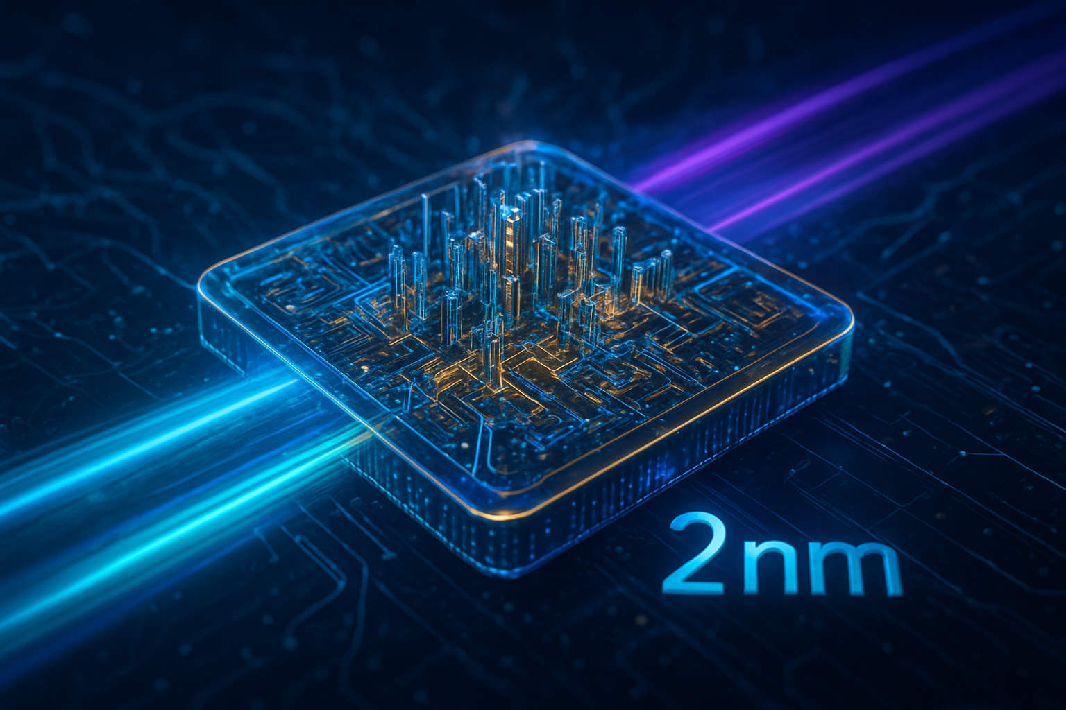
Redefining the Standard: The CDNA 4 Architecture and 3nm Innovation
At the heart of the MI350 series is the new CDNA 4 architecture, built on TSMC’s (NYSE:TSM) cutting-edge 3nm (N3P) process. This transition from the 5nm node used in the previous MI300 generation has allowed AMD to cram 185 billion transistors into its compute chiplets, representing a 21% increase in transistor density. The most striking technical advancement is the introduction of native support for ultra-low-precision FP4 and FP6 datatypes. These formats are essential for modern LLM inference, allowing for massive throughput increases without sacrificing the accuracy of the model's outputs.
The flagship MI355X is a direct assault on the specifications of NVIDIA’s B200. It boasts a staggering 288GB of HBM3E memory with 8 TB/s of bandwidth—roughly 1.6 times the capacity of a standard Blackwell GPU. This allows the MI355X to handle massive "KV caches," the temporary memory used by AI models to track long conversations or documents, far more effectively than its competitors. In terms of raw performance, the MI355X delivers 10.1 PFLOPs of peak AI performance (FP4/FP8 sparse), which AMD claims results in a 35x generational improvement in inference tasks compared to the MI300 series.
Initial reactions from the industry have been overwhelmingly positive, particularly regarding AMD's thermal management. The MI350X is designed for traditional air-cooled environments, while the high-performance MI355X utilizes Direct Liquid Cooling (DLC) to manage its 1400W power draw. Industry experts have noted that AMD's decision to maintain a consistent platform footprint allows data centers to upgrade from MI300 to MI350 with minimal infrastructure changes, a logistical advantage that NVIDIA’s more radical Blackwell rack designs sometimes lack.
A New Market Reality: Hyperscalers and the End of Monoculture
The launch of the MI350 series is already reshaping the strategic landscape for tech giants and AI startups alike. Meta Platforms (NASDAQ:META) has emerged as AMD’s most critical partner, deploying the MI350X at scale for its Llama 3.1 and early Llama 4 deployments. Meta’s pivot toward AMD is driven by its "PyTorch-first" infrastructure, which allows it to bypass NVIDIA’s proprietary software in favor of AMD’s open-source ROCm 7 stack. This move by Meta serves as a blueprint for other hyperscalers looking to reduce their reliance on a single hardware vendor.
Microsoft (NASDAQ:MSFT) and Oracle (NYSE:ORCL) have also integrated the MI350 series into their cloud offerings, with Azure’s ND MI350 v6 virtual machines now serving as a primary alternative to NVIDIA-based instances. For these cloud providers, the MI350 series offers a compelling economic proposition: AMD claims a 40% better "Tokens per Dollar" ratio than Blackwell systems. This cost efficiency is particularly attractive to AI startups that are struggling with the high costs of compute, providing them with a viable path to scale their services without the "NVIDIA tax."
Even the most staunch NVIDIA loyalists are beginning to diversify. In a significant market shift, both OpenAI and xAI have confirmed deep design engagements with AMD for the upcoming MI400 series. This indicates that the competitive pressure from AMD is forcing a "multi-sourcing" strategy across the entire AI ecosystem. As supply chain constraints for HBM3E continue to linger, having a second high-performance option like the MI350 series is no longer just a cost-saving measure—it is a requirement for operational resilience.
The Broader AI Landscape: From Training to Inference Dominance
The MI350 series arrives at a time when the AI landscape is maturing. While the initial "gold rush" focused on training massive foundational models, the industry's focus in late 2025 has shifted toward the sustainable deployment of these models. AMD’s 35x leap in inference performance aligns perfectly with this trend. By optimizing for the specific bottlenecks of inference—namely memory bandwidth and capacity—AMD is positioning itself as the "inference engine" of the world, leaving NVIDIA to defend its lead in the more specialized (but slower-growing) training market.
This development also highlights the success of the open-source software movement within AI. The rapid improvement of ROCm has largely neutralized the advantage NVIDIA held with CUDA. Because modern AI frameworks like JAX and PyTorch are now hardware-agnostic, the underlying silicon can be swapped with minimal friction. This "software-defined" hardware market is a major departure from previous semiconductor cycles, where software lock-in could protect a market leader for decades.
However, the rise of the MI350 series also brings concerns regarding power consumption and environmental impact. With the MI355X drawing up to 1400W, the energy demands of AI data centers continue to skyrocket. While AMD has touted improved performance-per-watt, the sheer scale of deployment means that energy availability remains the primary bottleneck for the industry. Comparisons to previous milestones, like the transition from CPUs to GPUs for general compute, suggest we are in the midst of a once-in-a-generation architectural shift that will define the power grid requirements of the next decade.
Looking Ahead: The Road to MI400 and Helios AI Racks
The MI350 series is merely a stepping stone in AMD’s aggressive annual release cycle. Looking toward 2026, AMD has already begun teasing the MI400 series, which is expected to utilize the CDNA "Next" architecture and HBM4 memory. The MI400 is projected to feature up to 432GB of memory per GPU, further extending AMD’s lead in capacity. Furthermore, AMD is moving toward a "rack-scale" strategy with its Helios AI Racks, designed to compete directly with NVIDIA’s GB200 NVL72.
The Helios platform will integrate the MI400 with AMD’s upcoming Zen 6 "Venice" EPYC CPUs and Pensando "Vulcano" 800G networking chips. This vertical integration is intended to provide a turnkey solution for exascale AI clusters, targeting a 10x performance improvement for Mixture of Experts (MoE) models. Experts predict that the battle for the "AI Rack" will be the next major frontier, as the complexity of interconnecting thousands of GPUs becomes the new primary challenge for AI infrastructure.
Conclusion: A Duopoly Reborn
The launch of the AMD Instinct MI350 series marks the official end of the NVIDIA monopoly in high-performance AI compute. By delivering a product that matches the Blackwell B200 in performance while offering superior memory and better cost efficiency, AMD has cemented its status as the definitive second source for AI silicon. This development is a win for the entire industry, as competition will inevitably drive down prices and accelerate the pace of innovation.
As we move into 2026, the key metric to watch will be the rate of enterprise adoption. While hyperscalers like Meta and Microsoft have already embraced AMD, the broader enterprise market—including financial services, healthcare, and manufacturing—is still in the early stages of its AI hardware transition. If AMD can continue to execute on its roadmap and maintain its software momentum, the MI350 series will be remembered as the moment the AI chip war truly began.
This content is intended for informational purposes only and represents analysis of current AI developments.
TokenRing AI delivers enterprise-grade solutions for multi-agent AI workflow orchestration, AI-powered development tools, and seamless remote collaboration platforms.
For more information, visit https://www.tokenring.ai/.