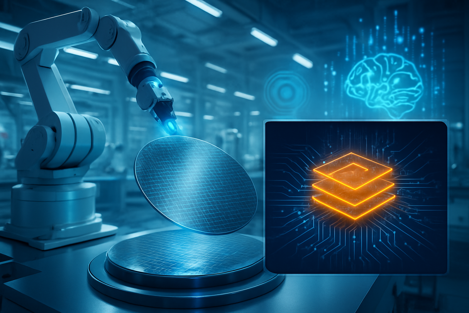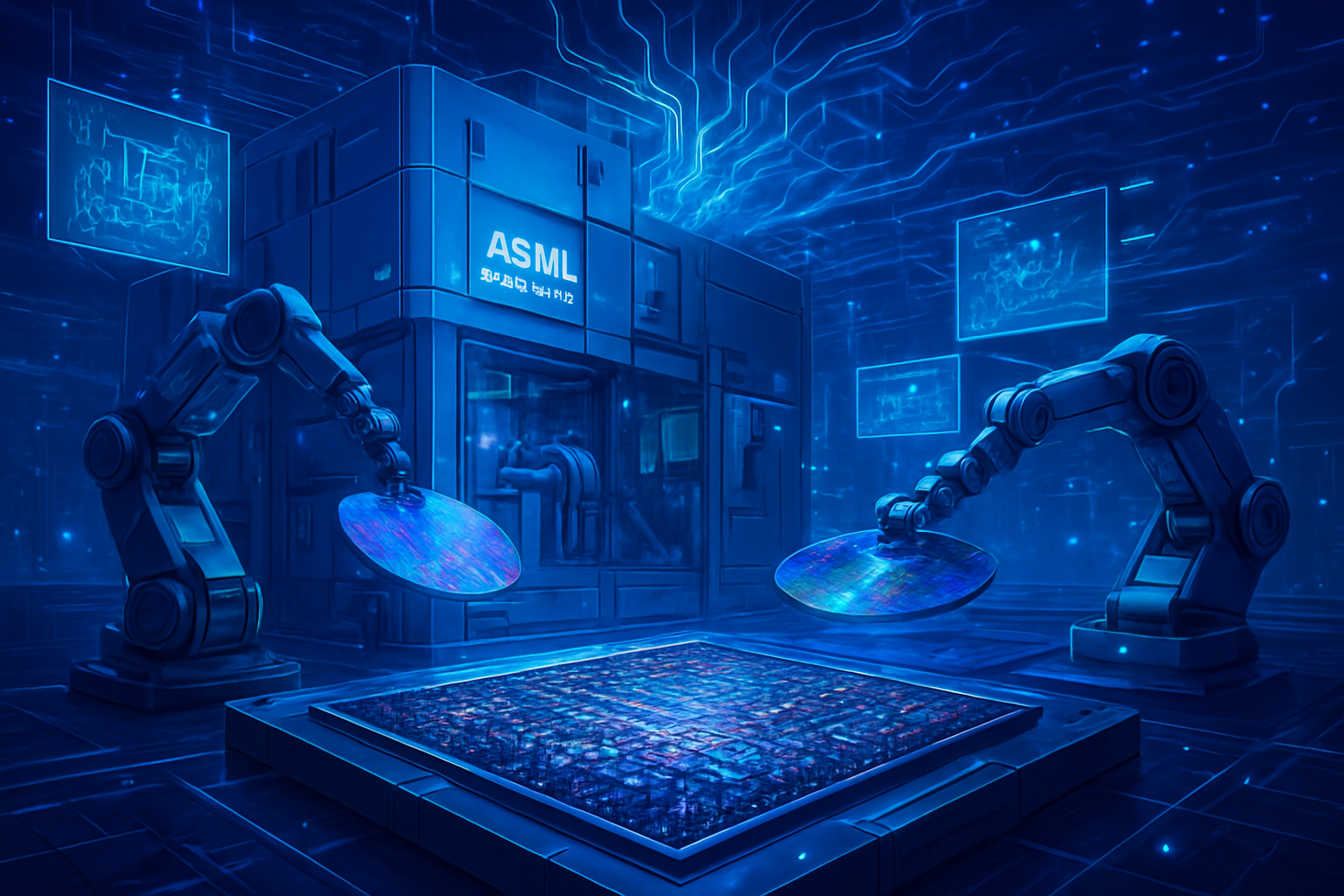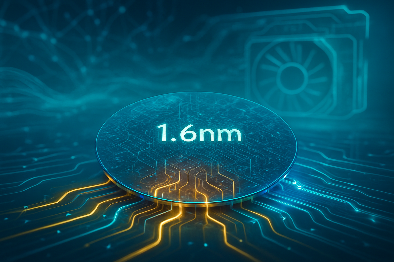
The semiconductor industry has officially crossed the threshold into the "Angstrom Era," a paradigm shift where transistor dimensions are no longer measured in nanometers but in the sub-nanometer scale. At the heart of this transition is Taiwan Semiconductor Manufacturing Company (NYSE: TSM), which has solidified its roadmap for the A16 process—a 1.6nm-class technology. With mass production scheduled to commence in late 2026, the A16 node represents more than just a shrink in scale; it introduces a radical re-architecting of how power is delivered to chips, catering specifically to the insatiable energy demands of next-generation artificial intelligence.
The immediate significance of the A16 announcement lies in its first confirmed major partner: NVIDIA (NASDAQ: NVDA). While Apple (NASDAQ: AAPL) has historically been the debut customer for TSMC’s cutting-edge nodes, reports from early 2026 indicate that NVIDIA has secured the initial capacity for its upcoming "Feynman" GPU architecture. This pivot underscores the central role that high-performance computing (HPC) now plays in driving the semiconductor industry, as the world moves toward massive AI models that require hardware capabilities far beyond current consumer-grade electronics.
The Super Power Rail: Redefining Transistor Efficiency
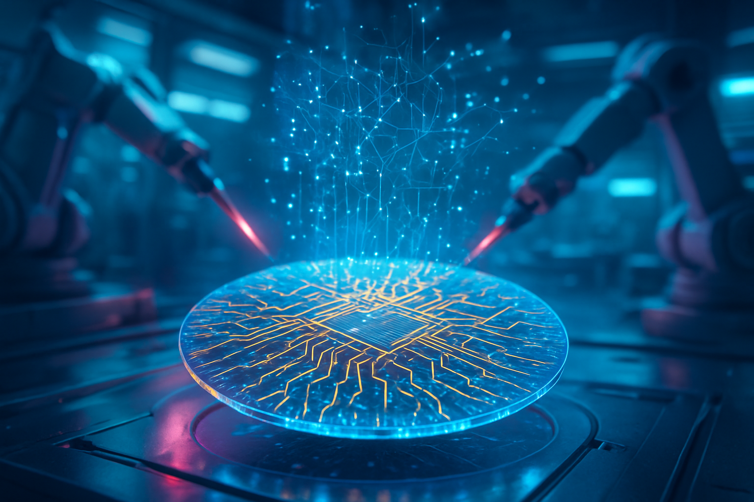
Technically, the A16 node is distinguished by the introduction of TSMC’s "Super Power Rail" (SPR) technology. This is a proprietary implementation of Backside Power Delivery Network (BSPDN), a method that moves the power distribution lines from the front side of the wafer to the back. In traditional chip design, power and signal lines compete for space on the top layers, leading to congestion and "IR drop"—a phenomenon where voltage is lost as it travels through complex wiring. By moving power to the backside, the Super Power Rail connects directly to the transistor’s source and drain, virtually eliminating these bottlenecks.
The shift to SPR provides staggering performance gains. Compared to the previous N2P (2nm) node, the A16 process offers an 8–10% improvement in speed at the same voltage or a 15–20% reduction in power consumption at the same speed. More importantly, the removal of power lines from the front of the chip frees up approximately 20% more space for signal routing, allowing for a 1.1x increase in transistor density. This architectural change is what allows A16 to leapfrog existing Gate-All-Around (GAA) implementations that still rely on front-side power.
Industry experts have reacted with a mix of awe and strategic calculation. The consensus is that while the 2nm node was a refinement of existing GAA technology, A16 is the true "breaking point" where physical limits necessitated a complete rethink of the chip's vertical stack. Unlike previous transitions that focused primarily on the transistor gate itself, A16 addresses the "wiring wall," ensuring that the increased density of the Angstrom Era doesn't result in a chip that is too power-hungry or heat-congested to function.
NVIDIA and the "Feynman" Gambit: A Strategic Shift in Foundry Leadership
The announcement that NVIDIA is likely the lead customer for A16 marks a historic shift in the foundry-client relationship. For over a decade, Apple was the undisputed king of TSMC’s "First-at-Node" status. However, as of early 2026, NVIDIA’s "Feynman" GPU architecture has become the industry's new North Star. Named after physicist Richard Feynman, this architecture is designed specifically for the post-Generative AI world, where clusters of thousands of GPUs work in unison.
NVIDIA is reportedly skipping the standard 2nm (N2) node for its most advanced accelerators, moving directly to A16 to leverage the Super Power Rail. This "node skip" is a strategic move driven by the thermal and power constraints of data centers. With modern AI racks consuming upwards of 2,000 watts, the 15-20% power efficiency gain from A16 is not just a benefit—it is a requirement for the continued scaling of large language models. The Feynman architecture will also integrate the Vera CPU (built on custom ARM-based "Olympus" cores) and utilize HBM4 or HBM5 memory, creating a tightly coupled ecosystem that maximizes the benefits of the 1.6nm process.
This development positions TSMC and NVIDIA as an almost unbreakable duo in the AI space, making it increasingly difficult for competitors to gain ground. By securing early A16 capacity, NVIDIA effectively locks in a multi-year performance advantage over rival chip designers who may still be grappling with the yields of 2nm or the complexities of competing processes. For TSMC, the partnership with NVIDIA provides a high-margin, high-volume anchor that justifies the multi-billion dollar investment in A16 fabs.
The Angstrom Arms Race: Intel, Samsung, and the Global Landscape
The broader AI landscape is currently witnessing a fierce "Angstrom Arms Race." While TSMC is targeting late 2026 for A16, Intel (NASDAQ: INTC) is pushing its 14A (1.4nm) process with a focus on ASML (NASDAQ: ASML) High-NA EUV lithography. Intel’s PowerVia technology—their version of backside power—actually beat TSMC to the market in a limited capacity at 18A, but TSMC’s A16 is widely seen as the more mature, high-yield solution for massive AI silicon. Samsung (KRX: 005930), meanwhile, is refining its 1.4nm (SF1.4) node, focusing on a four-nanosheet GAA structure to improve current drive.
This competition is crucial because it determines the physical limits of AI intelligence. The transition to the Angstrom Era signifies that we are reaching the end of traditional silicon scaling. The impacts are profound: as chip manufacturing becomes more expensive and complex, only a handful of "mega-corps" can afford to design for these nodes. This leads to concerns about market consolidation, where the barrier to entry for a new AI hardware startup is no longer just the software or the architecture, but the hundreds of millions of dollars required just to tape out a single 1.6nm chip.
Comparisons to previous milestones, like the move to FinFET at 22nm or the introduction of EUV at 7nm, suggest that the A16 transition is more disruptive. It is the first time that the "packaging" and the "power" of the chip have become as important as the transistor itself. In the coming years, the success of a company will be measured not just by how many transistors they can cram onto a die, but by how efficiently they can feed those transistors with electricity and clear the resulting heat.
Beyond A16: The Future of Silicon and Post-Silicon Scaling
Looking forward, the roadmap beyond 2026 points toward the 1.4nm and 1nm thresholds, where TSMC is already exploring the use of 2D materials like molybdenum disulfide (MoS2) and carbon nanotubes. Near-term, we can expect the A16 process to be the foundation for "Silicon Photonics" integration. As chip-to-chip communication becomes the primary bottleneck in AI clusters, integrating optical interconnects directly onto the A16 interposer will be the next major development.
However, challenges remain. The cost of manufacturing at the 1.6nm level is astronomical, and yield rates for the Super Power Rail will be the primary metric to watch throughout 2027. Experts predict that as we move toward 1nm, the industry may shift away from monolithic chips entirely, moving toward "3D-stacked" architectures where logic and memory are layered vertically to reduce latency. The A16 node is the essential bridge to this 3D future, providing the power delivery infrastructure necessary to support multi-layered chips.
Conclusion: A New Chapter in Computing History
The announcement of TSMC’s A16 roadmap and its late 2026 mass production marks the beginning of a new chapter in computing history. By integrating the Super Power Rail and securing NVIDIA as the vanguard customer for the Feynman architecture, TSMC has effectively set the pace for the entire technology sector. The move into the Angstrom Era is not merely a naming convention; it is a fundamental shift in semiconductor physics that prioritizes power delivery and interconnectivity as the primary drivers of performance.
As we look toward the latter half of 2026, the key indicators of success will be the initial yield rates of the A16 wafers and the first performance benchmarks of NVIDIA’s Feynman silicon. If TSMC can deliver on its efficiency promises, the gap between the leaders in AI and the rest of the industry will likely widen. The "Angstrom Era" is here, and it is being built on a foundation of backside power and the relentless pursuit of AI-driven excellence.
This content is intended for informational purposes only and represents analysis of current AI developments.
TokenRing AI delivers enterprise-grade solutions for multi-agent AI workflow orchestration, AI-powered development tools, and seamless remote collaboration platforms.
For more information, visit https://www.tokenring.ai/.