In a move that has fundamentally reshaped the competitive landscape of Silicon Valley, Apple (NASDAQ: AAPL) has officially moved on from its early alliance with OpenAI, signing a landmark $1 billion-per-year multi-year agreement with Google (NASDAQ: GOOGL). This strategic pivot establishes Google’s Gemini 2.5 Pro as the primary intelligence engine behind a completely overhauled Siri, signaling the end of Apple’s initial experiments with ChatGPT and the beginning of a new era for "Apple Intelligence."
The deal, finalized in January 2026, marks one of the most significant shifts in Apple’s modern history. By outsourcing the "brain" of its most personal interface to its longest-standing rival, Apple is betting that Google’s superior infrastructure and specialized Gemini models can provide the reliability and speed that Siri has long lacked. For Google, the agreement is a massive victory, securing its position as the foundational AI layer for the world’s most lucrative mobile ecosystem.
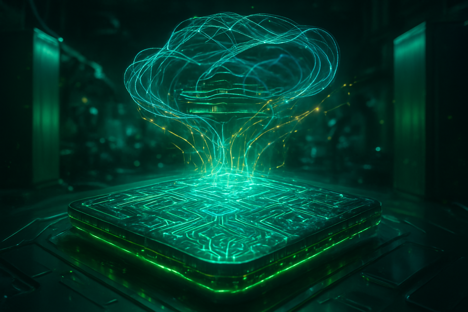
A Technical Resurrection: Siri’s 1.2 Trillion Parameter Brain
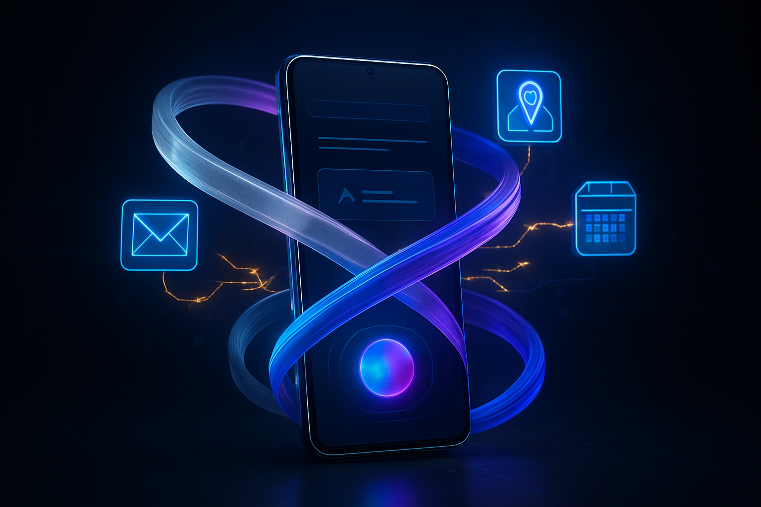
The revamped Siri, scheduled for a full rollout with iOS 26.4 this spring, represents a staggering leap in technical capabilities. While previous iterations of Siri struggled with basic intent and multi-step tasks, the new Gemini-powered assistant is built on a customized 1.2 trillion parameter model. According to internal benchmarks leaked prior to the announcement, the new Siri boasts a 92% success rate on complex, multi-app queries—a massive jump from the 58% recorded by the legacy architecture.
Technical specifications highlight a focus on "real-time fluid intelligence." Response times have been slashed to under 0.5 seconds, effectively removing the lag that has plagued voice assistants for a decade. The system also introduces a massive 128K context window (expandable to 1M tokens for specific tasks), allowing Siri to maintain "memory" of a conversation across weeks of interactions. This differs from previous approaches by utilizing a hybrid "on-device and off-device" routing system that determines if a request can be handled by Apple’s local Neural Engine or needs the heavy lifting of the Gemini 2.5 Pro model running in the cloud.
Initial reactions from the AI research community have been largely positive regarding the performance gains, though some experts have noted the irony of the situation. "Apple spent years building its own silicon to achieve vertical integration, only to realize that the scale of LLM training required a partner with Google’s data-center footprint," noted one senior researcher at Stanford’s Human-Centered AI Institute.
Strategic Realignment: The OpenAI Divorce and Google’s Return to Dominance
The shift from OpenAI to Google was not merely a technical choice but a strategic necessity born from a deteriorating relationship with Microsoft-backed (NASDAQ: MSFT) OpenAI. Reports indicate that OpenAI intentionally "walked away" from its primary partnership with Apple in late 2025. This move was reportedly driven by OpenAI’s desire to launch its own independent AI hardware, developed in collaboration with legendary former Apple designer Jony Ive, which would compete directly with the iPhone.
Google’s win in this "AI bake-off" provides Alphabet with a massive strategic advantage. By becoming the "intelligence layer" for iOS, Google ensures that its Gemini models are the default experience for over a billion users, effectively countering the threat of ChatGPT’s rise. This deal also reverses the historical cash flow between the two giants; while Google historically paid Apple billions to be the default search engine, Apple is now the one cutting checks to Google for AI licensing.
However, the competition is far from over. Microsoft has already begun pivoting its mobile strategy to focus on deep integration with specialized Android manufacturers, while smaller players like Anthropic and Perplexity are left to fight for the "pro-user" niche that Apple has now ceded to Google.
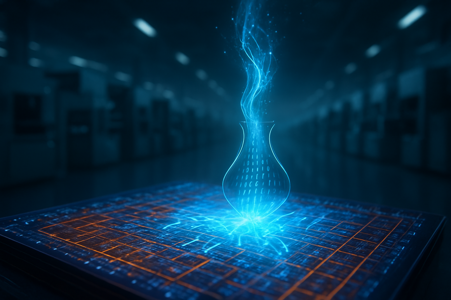
The Privacy Paradox and the "Cloud Conflict"
Perhaps the most scrutinized aspect of this $1 billion deal is its implication for user privacy. For years, Apple has marketed the iPhone as a sanctuary of personal data. To maintain this brand image, Apple is utilizing its "Private Cloud Compute" (PCC) architecture—a secure server system powered by Apple Silicon that acts as a buffer between the user and Google’s servers. Apple claims that Siri interactions sent to Gemini are anonymized and that data is never stored or used to train Google’s future models.
Despite these assurances, the partnership creates a "privacy paradox." In early February 2026, Google CEO Sundar Pichai referred to Google as Apple’s "preferred cloud provider," sparking concerns that advanced Siri features might eventually bypass Apple’s PCC to run directly on Google’s TPU-powered hardware for maximum performance. Privacy advocates warn that even if raw data is shielded, Siri will "inherit" Google’s biases and safety filters, effectively outsourcing the ethical and cognitive framework of the iPhone to a third party.
This move marks a departure from Apple’s traditional goal of total vertical integration. By relying on an external partner for core "reasoning" capabilities, Apple is acknowledging that the sheer computational cost of frontier AI models is a barrier that even the world’s most valuable company cannot overcome alone without sacrificing speed or battery life.
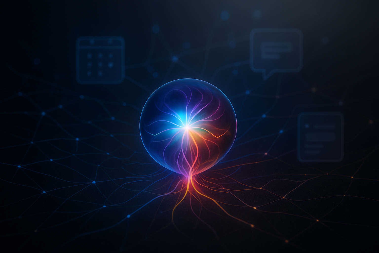
The Horizon: Agentic Siri and iOS 27
Looking ahead, the roadmap for this partnership points toward "Agentic Intelligence." In the near term, iOS 26.4 will introduce "Screen Awareness," allowing Siri to see and understand content across all apps in real-time. By September 2026, with the release of iOS 27, experts predict the arrival of "Siri 2.0"—a proactive agent capable of executing complex workflows without user intervention, such as automatically rebooking a canceled flight and notifying contacts based on the urgency of the user's calendar.
The primary challenge moving forward will be the "hallucination hurdle." While Gemini 2.5 Pro is highly capable, the stakes for a system with deep access to messages and emails are incredibly high. Experts predict that Apple will spend the next 18 months refining its "Guardrail Layer," a local filtering system designed to catch AI errors before they are presented to the user.
A New Chapter for Apple Intelligence
The Apple-Google deal represents a turning point in the history of artificial intelligence. It signals the end of the "experimentation phase" where tech giants flirted with various startups, and the beginning of a consolidated era where a few massive players control the foundational models that power our daily lives. Apple’s decision to pay $1 billion a year to Google is a pragmatic admission that in the AI arms race, infrastructure and data-center scale are the ultimate currencies.
The significance of this development cannot be overstated; it effectively marries the world’s best consumer hardware with the world’s most advanced search and reasoning engine. As we move into the spring of 2026, the tech industry will be watching closely to see if this "marriage of convenience" can deliver a Siri that finally lives up to its original promise—or if the privacy trade-offs will alienate Apple’s most loyal users.
This content is intended for informational purposes only and represents analysis of current AI developments.
TokenRing AI delivers enterprise-grade solutions for multi-agent AI workflow orchestration, AI-powered development tools, and seamless remote collaboration platforms.
For more information, visit https://www.tokenring.ai/.