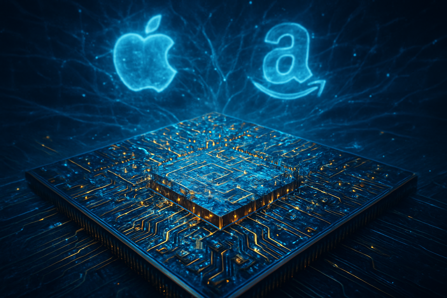
In a move that has sent shockwaves through Silicon Valley and effectively redrawn the map of the artificial intelligence landscape, Apple Inc. (NASDAQ: AAPL) and Alphabet Inc. (NASDAQ: GOOGL) officially announced a historic partnership on January 12, 2026. The deal establishes Google’s newly released Gemini 3 architecture as the primary intelligence layer for a completely overhauled Siri, marking the end of Apple’s decade-long struggle to build a world-class proprietary large language model. This "strategic realignment" positions the two tech giants as a unified front in the mobile AI era, a development that many analysts believe will define the next decade of personal computing.
The partnership, valued at an estimated $1 billion to $5 billion annually, represents a massive departure from Apple’s historically insular development strategy. Under the agreement, a custom-tuned, "white-labeled" version of Gemini 3 Pro will serve as the "Deep Intelligence Layer" for Apple Intelligence across the iPhone, iPad, and Mac ecosystems. While Apple will maintain its existing "opt-in" partnership with OpenAI for specific external queries, Gemini 3 will be the invisible engine powering Siri’s core reasoning, multi-step planning, and real-world knowledge. The immediate significance is clear: Apple has effectively "outsourced" the brain of its most important interface to its fiercest rival to ensure it does not fall behind in the race for autonomous AI agents.
Technical Foundations: The "Glenwood" Overhaul
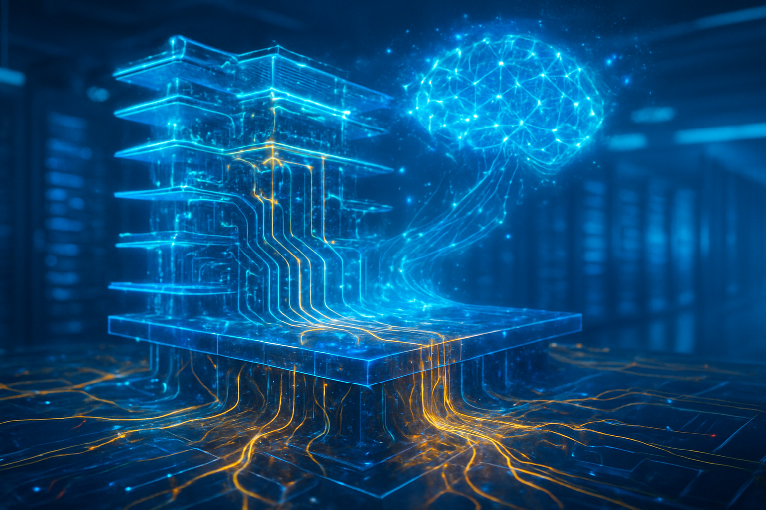
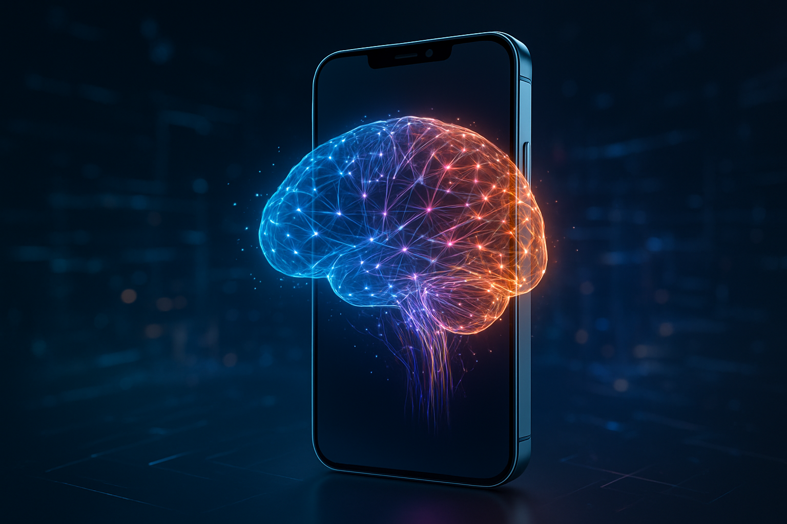
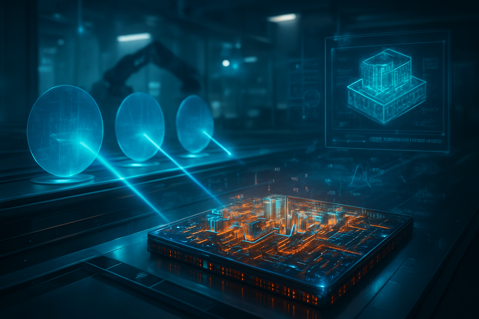
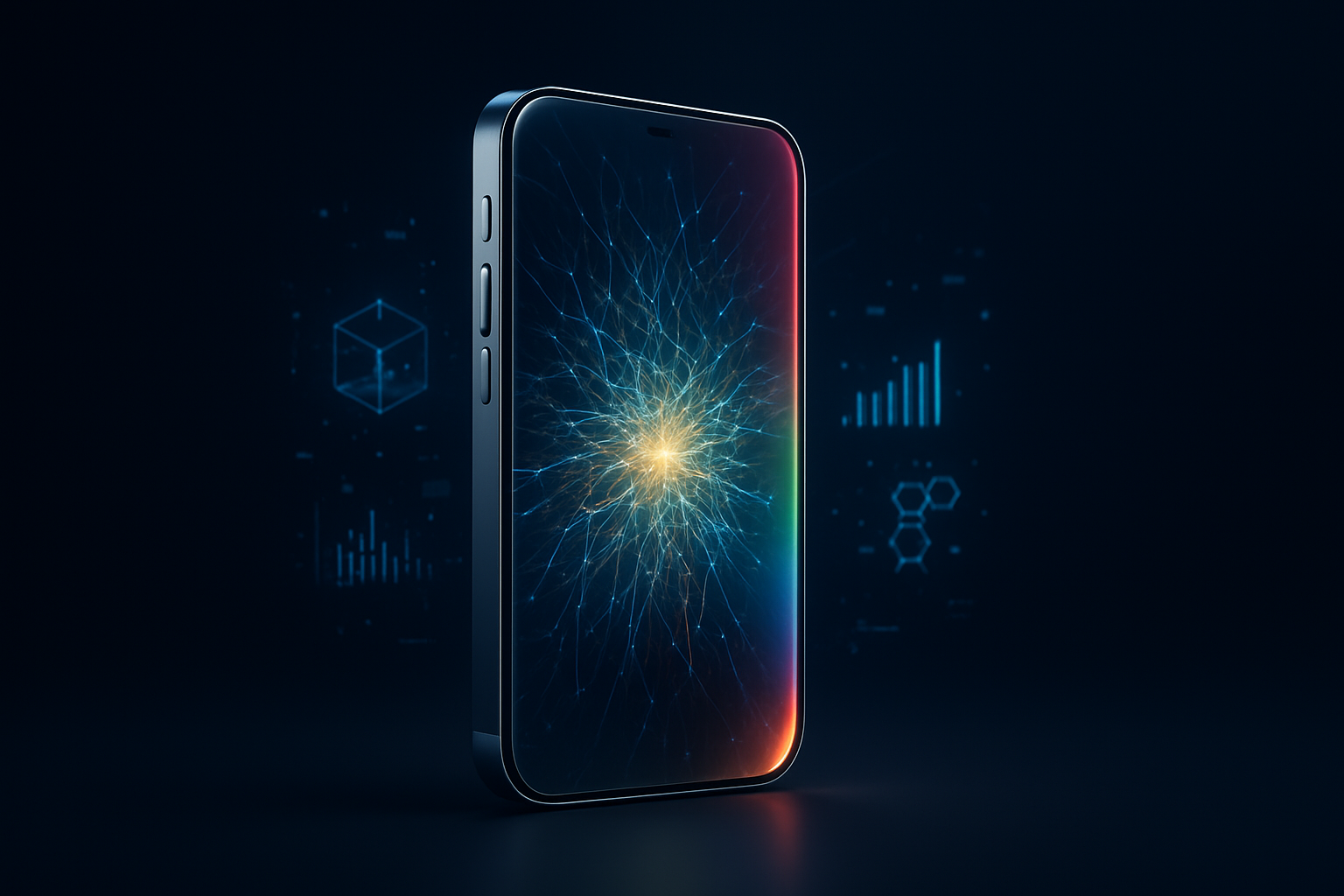
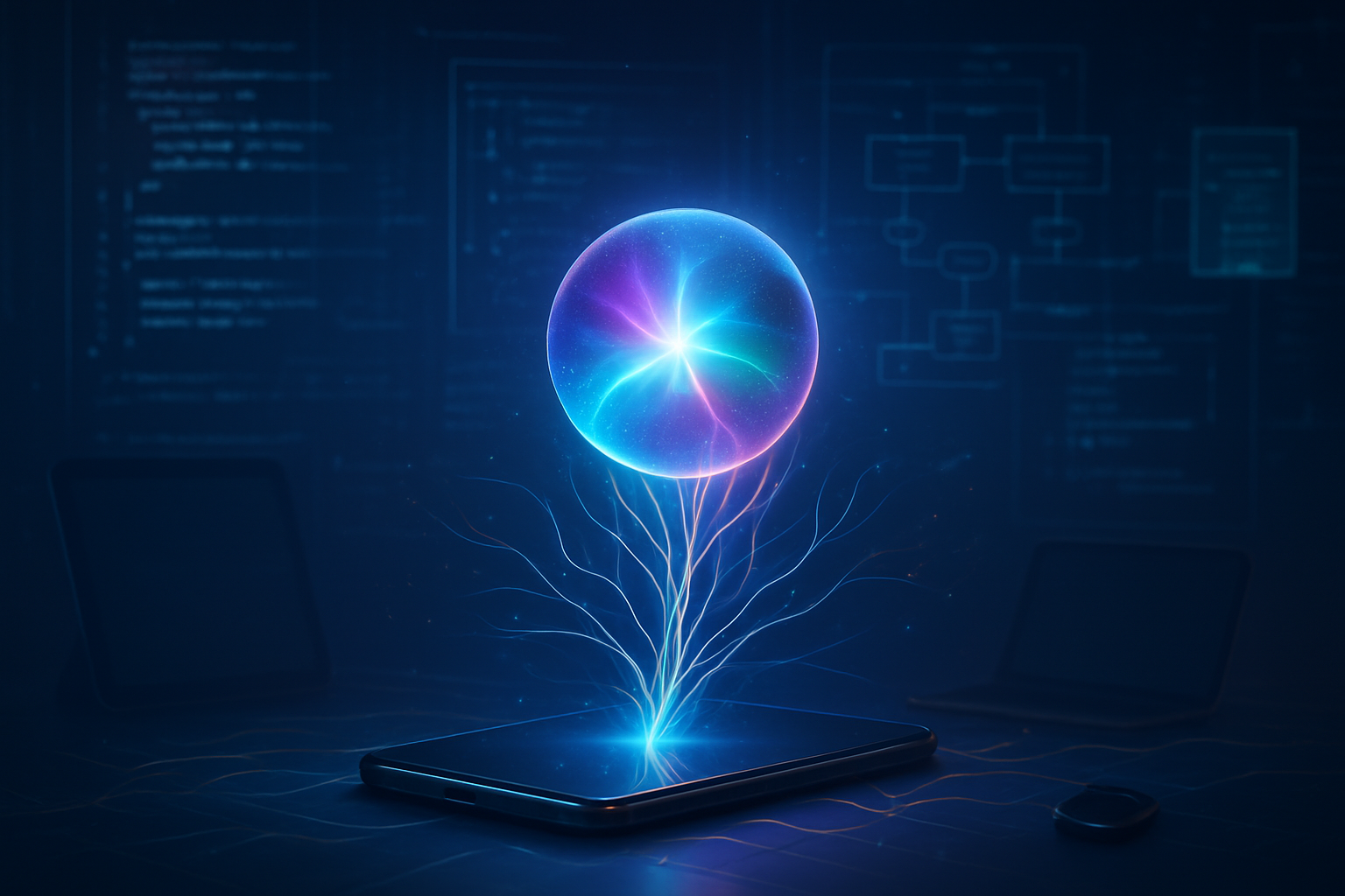
The revamped Siri, internally codenamed "Glenwood," represents a fundamental shift from a command-based assistant to a proactive, agentic digital companion. At its core is Gemini 3 Pro, a model Google released in late 2025 that boasts a staggering 1.2 trillion parameters and a context window of 1 million tokens. Unlike previous iterations of Siri that relied on rigid intent-matching, the Gemini-powered Siri can handle "agentic autonomy"—the ability to perform multi-step tasks across third-party applications. For example, a user can now command, "Find the hotel receipt in my emails, compare it to my bank statement, and file a reimbursement request in the company portal," and Siri will execute the entire workflow autonomously using Gemini 3’s advanced reasoning capabilities.
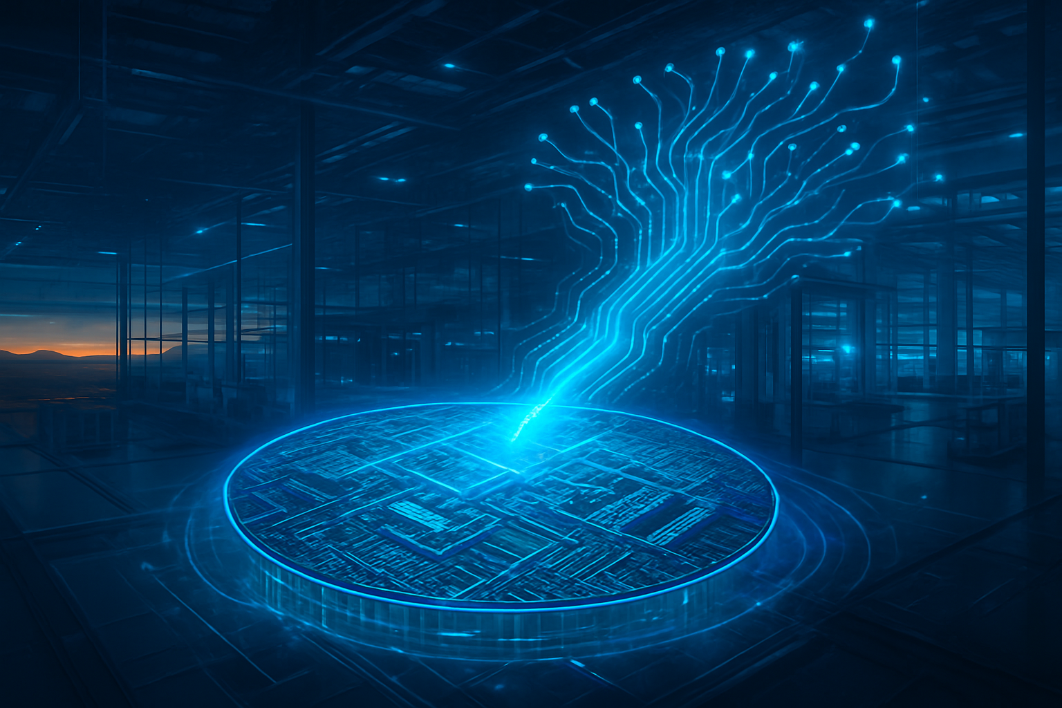
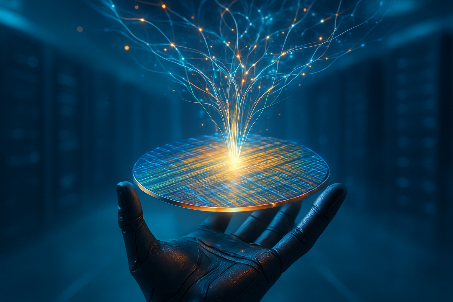
To address the inevitable privacy concerns, Apple is deploying Gemini 3 within its proprietary Private Cloud Compute (PCC) infrastructure. Rather than sending user data to Google’s public servers, the models run on Apple-owned "Baltra" silicon—a custom 3nm server chip developed in collaboration with Broadcom to handle massive inference demands without ever storing user data. This hybrid approach allows the A19 chip in the upcoming iPhone lineup to handle simple tasks on-device, while offloading complex "world knowledge" queries to the secure PCC environment. Initial reactions from the AI research community have been overwhelmingly positive, with many noting that Gemini 3 currently leads the LMArena leaderboard with a record-breaking 1501 Elo, significantly outperforming OpenAI’s GPT-5.1 in logical reasoning and math.
Strategic Impact: The AI Duopoly
The Apple-Google alliance has created an immediate "Code Red" situation for the Microsoft-OpenAI partnership. For the past three years, Microsoft Corp. (NASDAQ: MSFT) and OpenAI have enjoyed a first-mover advantage, but the integration of Gemini 3 into two billion active iOS devices effectively establishes a Google-Apple duopoly in the mobile AI market. Analysts from Wedbush Securities have noted that this deal shifts OpenAI into a "supporting role," where ChatGPT is likely to become a niche, opt-in feature rather than the foundational "brain" of the smartphone.
This shift has profound implications for the rest of the industry. Microsoft, realizing it may be boxed out of the mobile assistant market, has reportedly pivoted its "Copilot" strategy to focus on an "Agentic OS" for Windows 11, doubling down on enterprise and workplace automation. Meanwhile, OpenAI is rumored to be accelerating its own hardware ambitions. Reports suggest that CEO Sam Altman and legendary designer Jony Ive are fast-tracking a project codenamed "Sweet Pea"—a screenless, AI-first wearable designed to bypass the smartphone entirely and compete directly with the Gemini-powered Siri. The deal also places immense pressure on Meta and Anthropic, who must now find distribution channels that can compete with the sheer scale of the iOS and Android ecosystems.
Broader Significance: From Chatbots to Agents
This partnership is more than just a corporate deal; it marks the transition of the broader AI landscape from the "Chatbot Era" to the "Agentic Era." For years, AI was a destination—a website or app like ChatGPT that users visited to ask questions. With the Gemini-powered Siri, AI becomes an invisible fabric woven into the operating system. This mirrors the transition from the early web to the mobile app revolution, where convenience and integration eventually won over raw capability. By choosing Gemini 3, Apple is prioritizing a "curator" model, where it manages the user experience while leveraging the most powerful "world engine" available.
However, the move is not without its potential concerns. The partnership has already reignited antitrust scrutiny from regulators in both the U.S. and the EU, who are investigating whether the deal effectively creates an "unbeatable moat" that prevents smaller AI startups from reaching consumers. Furthermore, there are questions about dependency; by relying on Google for its primary intelligence layer, Apple risks losing the ability to innovate on the foundational level of AI. This is a significant pivot from Apple's usual philosophy of owning the "core technologies" of its products, signaling just how high the stakes have become in the generative AI race.
Future Developments: The Road to iOS 20 and Beyond
In the near term, consumers can expect a gradual rollout of these features, with the full "Glenwood" overhaul scheduled to hit public release in March 2026 alongside iOS 19.4. Developers are already being briefed on new SDKs that will allow their apps to "talk" directly to Siri’s Gemini 3 engine, enabling a new generation of apps that are designed primarily for AI agents rather than human eyes. This "headless" app trend is expected to be a major theme at Apple’s WWDC in June 2026.
As we look further out, the industry predicts a "hardware supercycle" driven by the need for more local AI processing power. Future iPhones will likely require a minimum of 16GB of RAM and dedicated "Neural Storage" to keep up with the demands of an autonomous Siri. The biggest challenge remaining is the "hallucination problem" in agentic workflows; if Siri autonomously files an expense report with incorrect data, the liability remains a gray area. Experts believe the next two years will be focused on "Verifiable AI," where models like Gemini 3 must provide cryptographic proof of their reasoning steps to ensure accuracy in autonomous tasks.
Conclusion: A Tectonic Shift in Technology History
The Apple-Google Gemini 3 partnership will likely be remembered as the moment the AI industry consolidated into its final form. By combining Apple’s unparalleled hardware-software integration with Google’s leading-edge research, the two companies have created a formidable platform that will be difficult for any competitor to dislodge. The deal represents a pragmatic admission by Apple that the pace of AI development is too fast for even the world’s most valuable company to tackle alone, and a massive victory for Google in its quest for AI dominance.
In the coming weeks and months, the tech world will be watching closely for the first public betas of the new Siri. The success or failure of this integration will determine whether the smartphone remains the center of our digital lives or if we are headed toward a post-app future dominated by ambient, wearable AI. For now, one thing is certain: the "Siri is stupid" era is officially over, and the era of the autonomous digital agent has begun.
This content is intended for informational purposes only and represents analysis of current AI developments.
TokenRing AI delivers enterprise-grade solutions for multi-agent AI workflow orchestration, AI-powered development tools, and seamless remote collaboration platforms.
For more information, visit https://www.tokenring.ai/.