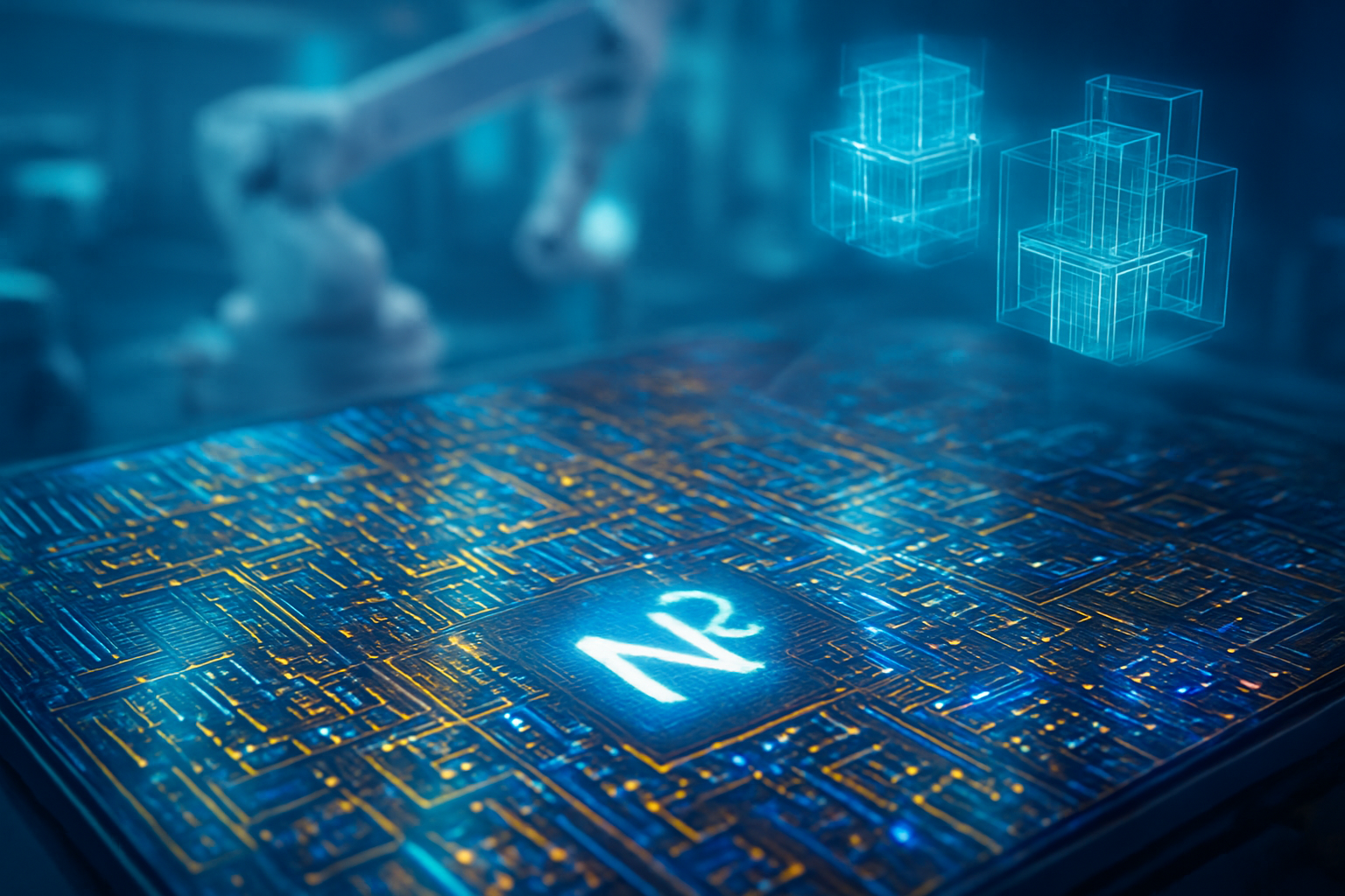
As of today, January 13, 2026, the global semiconductor landscape has officially shifted on its axis. Taiwan Semiconductor Manufacturing Company (NYSE: TSM) has announced that its Fab 22 facility in Kaohsiung has reached high-volume manufacturing (HVM) for its long-awaited 2nm (N2) process node. This milestone marks the definitive end of the FinFET transistor era and the beginning of a new chapter in silicon architecture that promises to redefine the limits of performance, efficiency, and artificial intelligence.
The transition to 2nm is not merely an incremental step; it is a foundational reset of the "Golden Rule" of Moore's Law. By successfully ramping up production at Fab 22 alongside its sister facility, Fab 20 in Hsinchu, TSMC is now delivering the world’s most advanced semiconductors at a scale that its competitors—namely Samsung and Intel—are still struggling to match. With yields already reported in the 65–70% range, the 2nm era is arriving with a level of maturity that few industry analysts expected so early in the year.
The GAA Revolution: Breaking the Power Wall
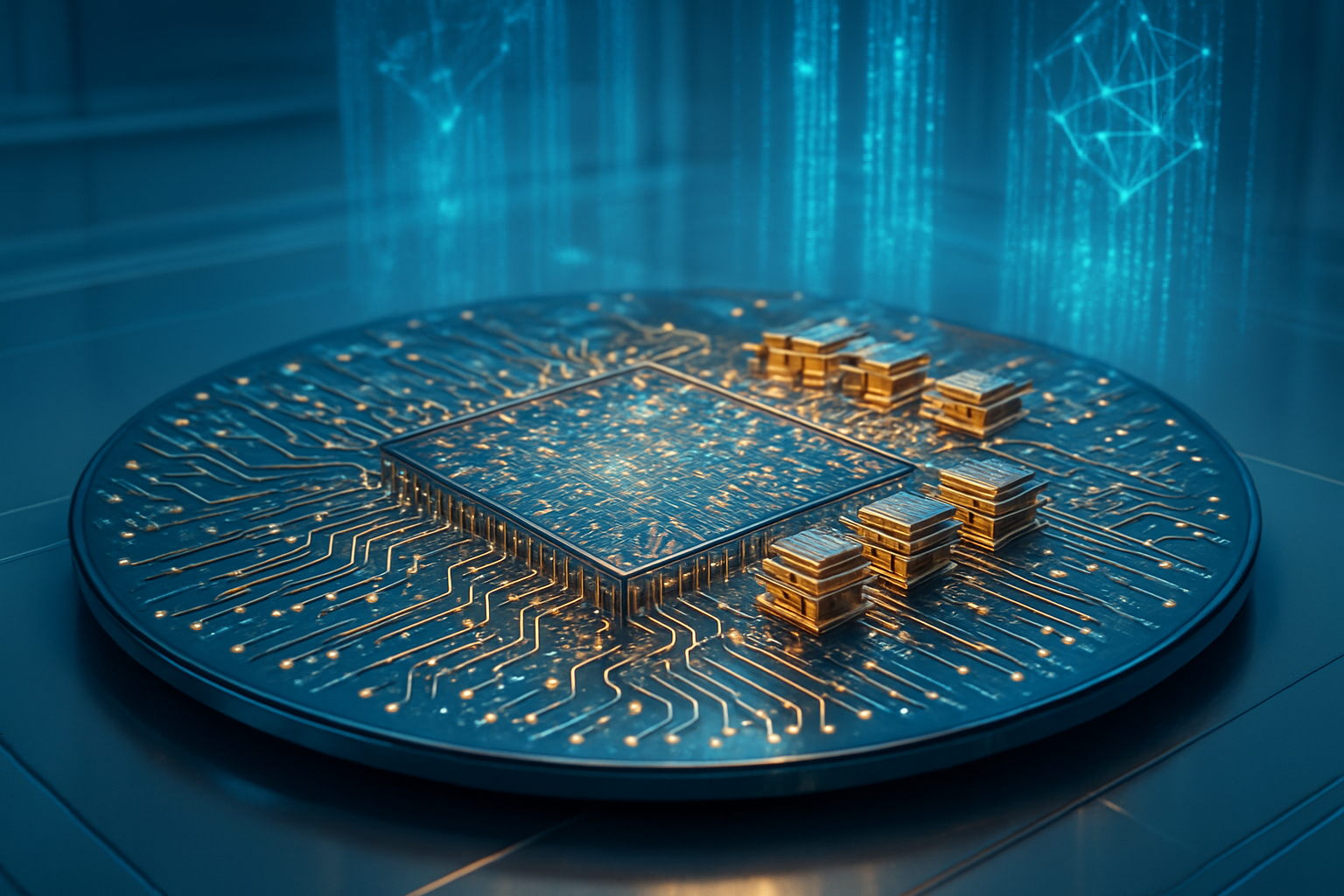
The technical centerpiece of the N2 node is the transition from FinFET (Fin Field-Effect Transistor) to Gate-All-Around (GAA) Nanosheet transistors. For over a decade, FinFET served the industry well, but as transistors shrank toward the atomic scale, current leakage and electrostatic control became insurmountable hurdles. The GAA architecture solves this by wrapping the gate around all four sides of the channel, providing a degree of control that was previously impossible. This structural shift allows for a staggering 25% to 30% reduction in power consumption at the same performance levels compared to the previous 3nm (N3E) generation.
Beyond power savings, the N2 process offers a 10% to 15% performance boost at the same power envelope, alongside a logic density increase of up to 20%. This is achieved through the stacking of horizontal silicon ribbons, which allows for more current to flow through a smaller footprint. Initial reactions from the semiconductor research community have been overwhelmingly positive, with experts noting that TSMC has effectively bypassed the "yield valley" that often plagues such radical architectural shifts. The ability to maintain high yields while implementing GAA is being hailed as a masterclass in precision engineering.
Apple’s $30,000 Wafers and the 50% Capacity Lock
The commercial implications of this rollout are being felt immediately across the consumer electronics sector. Apple (NASDAQ: AAPL) has once again flexed its capital muscle, reportedly securing a massive 50% of TSMC’s total 2nm capacity through the end of 2026. This reservation is earmarked for the upcoming A20 Pro chip, which will power the iPhone 18 Pro and Apple’s highly anticipated first-generation foldable device. By locking up half of the world's most advanced silicon, Apple has created a formidable "supply-side barrier" that leaves rivals like Qualcomm and MediaTek scrambling for the remaining capacity.
This strategic move gives Apple a multi-generational lead in performance-per-watt, particularly in the realm of on-device AI. At an estimated cost of $30,000 per wafer, the N2 node is the most expensive in history, yet the premium is justified by the strategic advantage it provides. For tech giants and startups alike, the message is clear: the 2nm era is a high-stakes game where only those with the deepest pockets and the strongest foundry relationships can play. This further solidifies TSMC’s near-monopoly on advanced logic, as it currently produces an estimated 95% of the world’s most sophisticated AI chips.
Fueling the AI Super-Cycle: From Data Centers to the Edge
The arrival of 2nm silicon is the "pressure release valve" the AI industry has been waiting for. As Large Language Models (LLMs) scale toward tens of trillions of parameters, the energy cost of training and inference has hit a "power wall." The 30% efficiency gain offered by the N2 node allows data center operators to pack significantly more compute density into their existing power footprints. This is critical for companies like NVIDIA (NASDAQ: NVDA) and AMD (NASDAQ: AMD), who are already racing to port their next-generation AI accelerators to the N2 process to maintain their dominance in the generative AI space.
Perhaps more importantly, the N2 node is the catalyst for the "Edge AI" revolution. By providing the efficiency needed to run complex generative tasks locally on smartphones and PCs, 2nm chips are enabling a new class of "AI-first" devices. This shift reduces the reliance on cloud-based processing, improving latency and privacy while triggering a massive global replacement cycle for hardware. The 2nm era isn't just about making chips smaller; it's about making AI ubiquitous, moving it from massive server farms directly into the pockets of billions of users.
The Path to 1.4nm and the High-NA EUV Horizon
Looking ahead, TSMC is already laying the groundwork for the next milestones. While the current N2 node utilizes standard Extreme Ultraviolet (EUV) lithography, the company is preparing for the introduction of "N2P" and the "A16" (1.6nm) nodes, which will introduce "backside power delivery"—a revolutionary method of routing power from the bottom of the wafer to reduce interference and further boost efficiency. These developments are expected to enter the pilot phase by late 2026, ensuring that the momentum of the 2nm launch carries directly into the next decade of innovation.
The industry is also watching for the integration of High-NA (Numerical Aperture) EUV machines. While TSMC has been more cautious than Intel in adopting these $350 million machines, the complexity of 2nm and beyond will eventually make them a necessity. The challenge remains the astronomical cost of manufacturing; as wafer prices climb toward $40,000 in the 1.4nm era, the industry must find ways to balance cutting-edge performance with economic viability. Experts predict that the next two years will be defined by a "yield war," where the ability to manufacture these complex designs at scale will determine the winners of the silicon race.
A New Benchmark in Semiconductor History
TSMC’s successful ramp-up at Fab 22 is more than a corporate victory; it is a landmark event in the history of technology. The transition to GAA Nanosheets at the 2nm level represents the most significant architectural change since the introduction of FinFET in 2011. By delivering a 30% power reduction and securing the hardware foundation for the AI super-cycle, TSMC has once again proven its role as the indispensable engine of the modern digital economy.
In the coming weeks and months, the industry will be closely monitoring the first benchmarks of the A20 Pro silicon and the subsequent announcements from NVIDIA regarding their N2-based Blackwell successors. As the first 2nm wafers begin their journey from Kaohsiung to assembly plants around the world, the tech industry stands on the precipice of a new era of compute. The "2nm era" has officially begun, and the world of artificial intelligence will never be the same.
This content is intended for informational purposes only and represents analysis of current AI developments.
TokenRing AI delivers enterprise-grade solutions for multi-agent AI workflow orchestration, AI-powered development tools, and seamless remote collaboration platforms.
For more information, visit https://www.tokenring.ai/.