As 2026 dawns, the technology industry is witnessing what analysts are calling the most significant hardware upgrade cycle in over a decade. Driven by the full-scale deployment of Apple Intelligence, the "AI Supercycle" has moved from a marketing buzzword to a tangible market reality. At the heart of this shift is the iPhone 17 Pro, a device that has fundamentally changed the consumer relationship with mobile technology by transitioning the smartphone from a passive tool into a proactive, agentic companion.
The release of the iPhone 17 Pro in late 2025, coupled with the groundbreaking iOS 26 software architecture, has triggered a massive wave of device replacements. For the first time, the value proposition of a new smartphone is defined not by the quality of its camera or the brightness of its screen, but by its "Neural Capacity"—the ability to run sophisticated, multi-step AI agents locally without compromising user privacy.
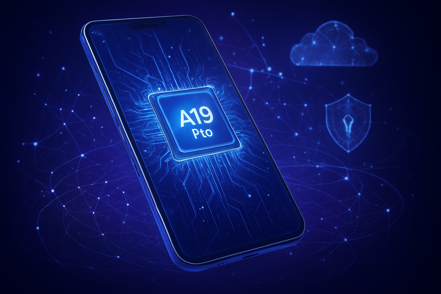
Technical Powerhouse: The A19 Pro and the 12GB RAM Standard
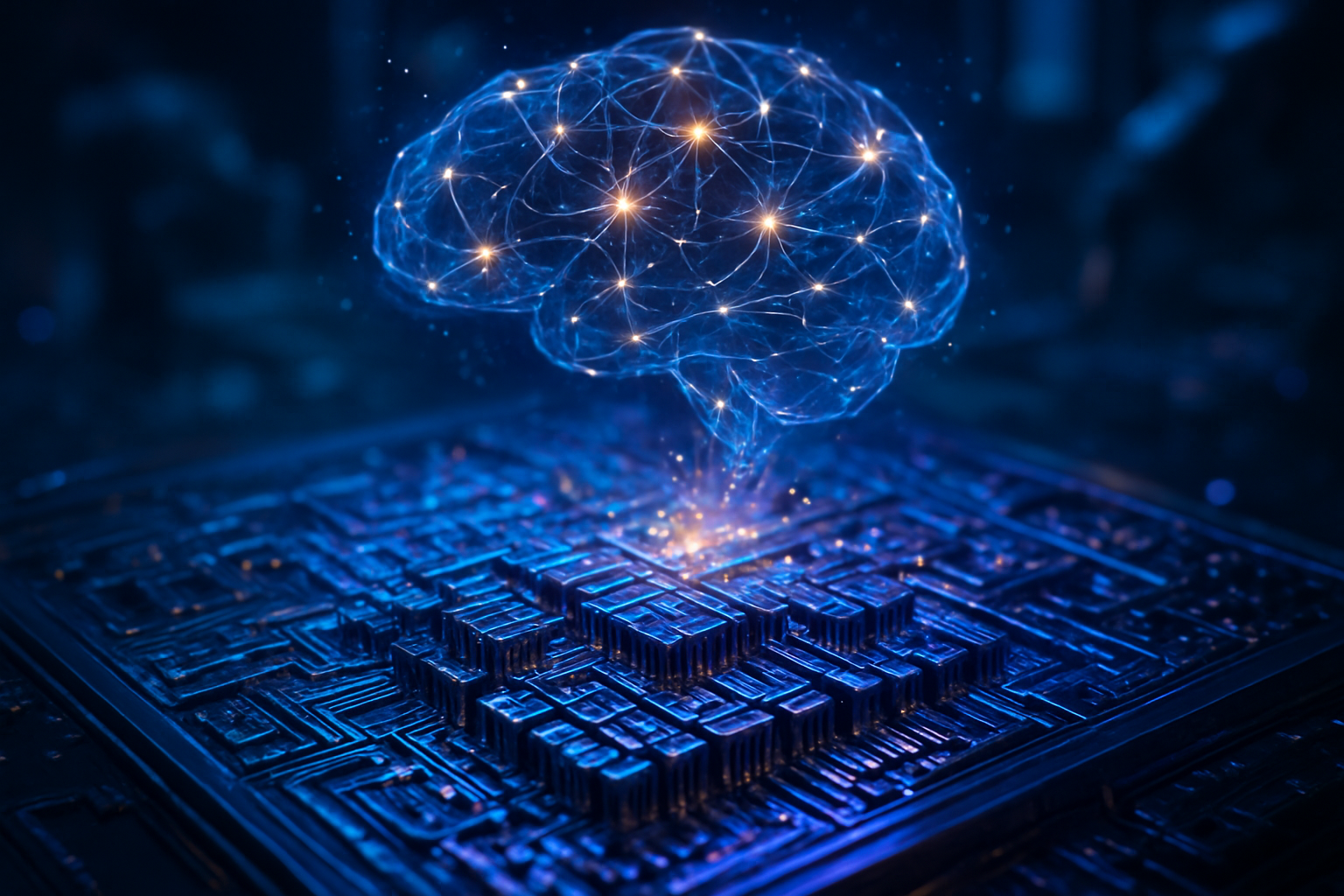
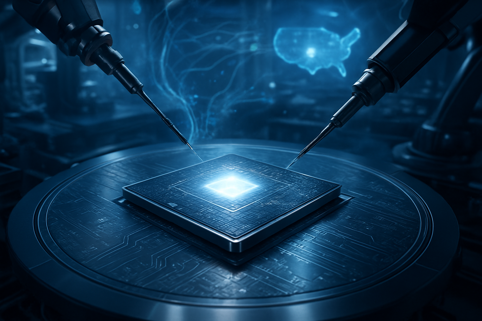
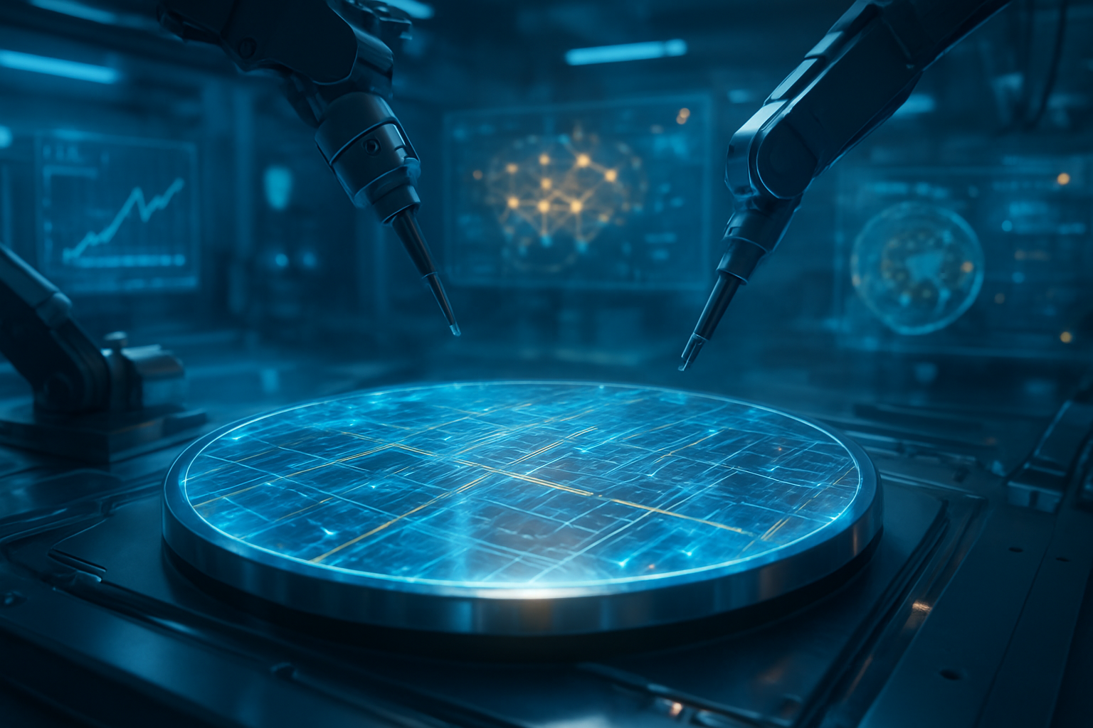
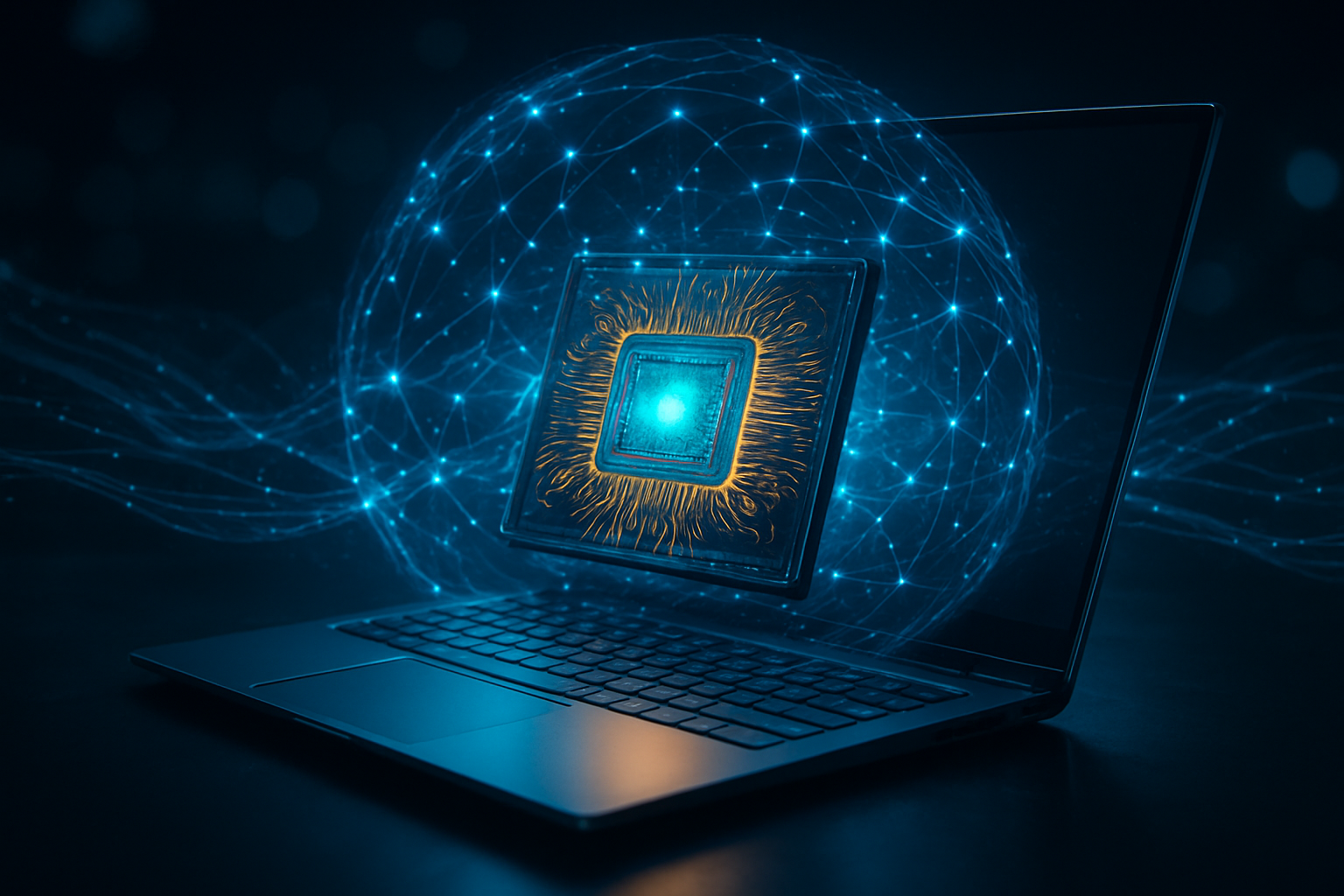
The technological foundation of this supercycle is the A19 Pro chip, manufactured on TSMC’s refined 3nm (N3P) process. While previous chip iterations focused on incremental gains in peak clock speeds, the A19 Pro delivers a staggering 40% boost in sustained performance. This leap is not merely a result of transistor density but a fundamental redesign of the iPhone’s internal architecture. For the first time, Apple (NASDAQ: AAPL) has integrated a vapor chamber cooling system into the Pro lineup, allowing the A19 Pro to maintain high-performance states for extended periods during intensive local LLM (Large Language Model) processing.
To support these advanced AI capabilities, Apple has established 12GB of LPDDR5X RAM as the new baseline for the Pro series. This memory expansion was a technical necessity for "local agentic intelligence." Unlike the 8GB models of the previous generation, the 12GB configuration allows the iPhone 17 Pro to keep a 3-billion-parameter language model resident in its memory. This ensures that the device can perform complex tasks—such as real-time language translation, semantic indexing of a user's entire file system, and on-device image generation—with zero latency and without needing to ping a remote server.
Initial reactions from the AI research community have been overwhelmingly positive, particularly regarding Apple's "Neural Accelerators" integrated directly into the GPU cores. Industry experts note that this approach differs significantly from competitors who often rely on cloud-heavy processing. By prioritizing local execution, Apple has effectively bypassed the "latency wall" that has hindered the adoption of voice-based AI assistants in the past, making the new Siri feel instantaneous and conversational.
Market Dominance and the Competitive Moat
The 2026 supercycle has placed Apple in a dominant strategic position, forcing competitors like Samsung and Google (NASDAQ: GOOGL) to accelerate their own on-device AI roadmaps. By tightly coupling its custom silicon with the iOS 26 ecosystem, Apple has created a "privacy moat" that is difficult for data-driven advertising companies to replicate. The integration of Private Cloud Compute (PCC) has been the masterstroke in this strategy; when a task exceeds the iPhone’s local processing power, it is handed off to Apple Silicon-based servers in a "stateless" environment where data is never stored and is mathematically inaccessible to Apple itself.
This development has caused a significant disruption in the app economy. Traditional apps are increasingly being replaced by "intent-based" interactions where users interact with Siri rather than opening individual applications. This shift has forced developers to move away from traditional UI design and toward "App Intents," ensuring their services are discoverable by the iOS 26 agentic engine. Tech giants that rely on high "time-in-app" metrics are now pivoting to ensure they remain relevant in a world where the OS, not the app, manages the user’s workflow.
A New Paradigm: Agentic Siri and Privacy-First AI
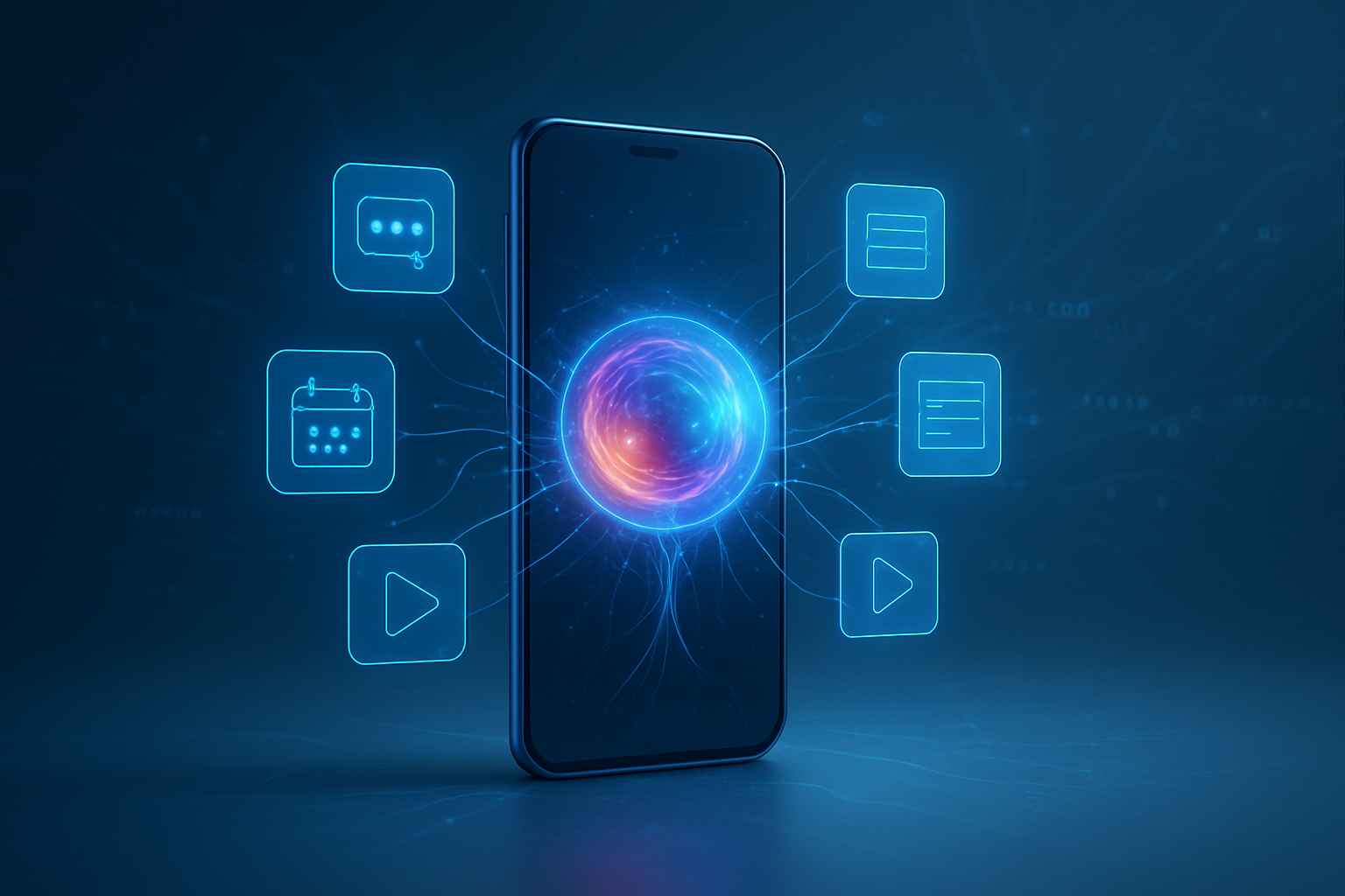
The broader significance of the 2026 AI Supercycle lies in the evolution of Siri from a voice-activated search tool into a multi-step digital agent. Within the iOS 26 framework, Siri is now capable of executing complex, cross-app sequences. A user can provide a single prompt like, "Find the contract I received in Mail yesterday, highlight the changes in the indemnity clause, and draft a summary for my legal team in Slack," and the system handles the entire chain of events autonomously. This is made possible by "Semantic Indexing," which allows the AI to understand the context and relationships between data points across different applications.
This milestone marks a departure from the "chatbot" era of 2023 and 2024. The societal impact is profound, as it democratizes high-level productivity tools that were previously the domain of power users. However, this advancement has also raised concerns regarding "algorithmic dependency." As users become more reliant on AI agents to manage their professional and personal lives, questions about the transparency of the AI’s decision-making process and the potential for "hallucinated" actions in critical workflows remain at the forefront of public debate.
The Road Ahead: iOS 26.4 and the Future of Human-AI Interaction
Looking forward to the rest of 2026, the industry is anticipating the release of iOS 26.4, which is rumored to introduce "Proactive Anticipation" features. This would allow the iPhone to suggest and even pre-execute tasks based on a user’s habitual patterns and real-time environmental context. For example, if the device detects a flight delay, it could automatically notify contacts, reschedule calendar appointments, and book a ride-share without the user needing to initiate the request.
The long-term challenge for Apple will be maintaining the delicate balance between utility and privacy. As Siri becomes more deeply embedded in the user’s digital life, the volume of sensitive data processed by Private Cloud Compute will grow exponentially. Experts predict that the next frontier will involve "federated learning," where the AI models themselves are updated and improved based on user interactions without the raw data ever leaving the individual’s device.
Closing the Loop on the AI Supercycle
The 2026 AI Supercycle represents a watershed moment in the history of personal computing. By combining the 40% performance boost of the A19 Pro with the 12GB RAM standard and the agentic capabilities of iOS 26, Apple has successfully transitioned the smartphone into the "Intelligence" era. The key takeaway for the industry is that hardware still matters; the most sophisticated software in the world is limited by the silicon it runs on, and Apple’s vertical integration has allowed it to set a new bar for what a mobile device can achieve.
As we move through the first quarter of 2026, the focus will remain on how effectively these AI agents can handle the complexities of the real world. The significance of this development cannot be overstated—it is the moment when AI stopped being a feature and started being the interface. For consumers and investors alike, the coming months will be a test of whether this new "Personal Intelligence" can deliver on its promise of a more efficient, privacy-focused digital future.
This content is intended for informational purposes only and represents analysis of current AI developments.
TokenRing AI delivers enterprise-grade solutions for multi-agent AI workflow orchestration, AI-powered development tools, and seamless remote collaboration platforms.
For more information, visit https://www.tokenring.ai/.