Tag: Arizona Tech

  • TSMC’s Arizona “Gigafab Cluster” Scales Up with $165 Billion Total Investment

    TSMC’s Arizona “Gigafab Cluster” Scales Up with $165 Billion Total Investment

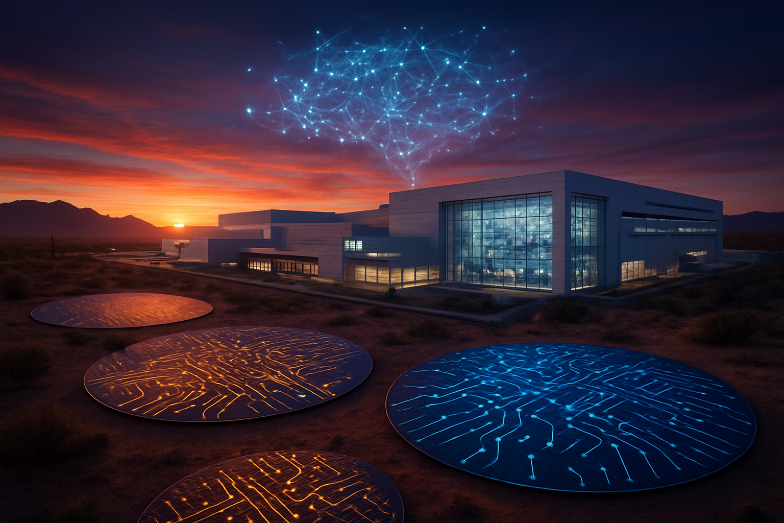
    In a move that fundamentally reshapes the global semiconductor landscape, Taiwan Semiconductor Manufacturing Company (NYSE: TSM) has dramatically accelerated its expansion in the United States. The company recently announced an additional $100 billion commitment, elevating its total investment in Phoenix, Arizona, to a staggering $165 billion. This massive infusion of capital transforms the site from a series of individual factories into a cohesive "Gigafab Cluster," signaling a new era of American-made high-performance computing.

    The scale of the project is unprecedented in the history of U.S. foreign direct investment. By scaling up to six advanced wafer manufacturing plants and adding two dedicated advanced packaging facilities, TSMC is positioning its Arizona hub as the primary engine for the next generation of artificial intelligence. This strategic pivot ensures that the most critical components for AI—ranging from the processors powering data centers to the chips inside consumer devices—can be manufactured, packaged, and shipped entirely within the United States.

    Technical Milestones: From 4nm to the Angstrom Era

    The technical specifications of the Arizona "Gigafab Cluster" represent a significant leap forward for domestic chip production. While the project initially focused on 5nm and 4nm nodes, the newly expanded roadmap brings TSMC’s most advanced technologies to U.S. soil nearly simultaneously with their Taiwanese counterparts. Fab 1 has already entered high-volume manufacturing using 4nm (N4P) technology as of late 2024. However, the true "crown jewels" of the cluster will be Fabs 3 and 4, which are now designated for 2nm and the revolutionary A16 (1.6nm) process technologies.

    The A16 node is particularly significant for the AI industry, as it introduces TSMC’s "Super Power Rail" architecture. This backside power delivery system separates signal and power wiring, drastically reducing voltage drop and enhancing energy efficiency—a critical requirement for the power-hungry GPUs used in large language model training. Furthermore, the addition of two advanced packaging facilities addresses a long-standing "bottleneck" in the U.S. supply chain. By integrating CoWoS (Chip-on-Wafer-on-Substrate) and SoIC (System-on-Integrated-Chips) capabilities on-site, TSMC can now offer a "one-stop shop" for advanced silicon, eliminating the need to ship wafers back to Asia for final assembly.

    To support this massive scale-up, TSMC recently completed its second major land acquisition in North Phoenix, adding 900 acres to its existing 1,100-acre footprint. This 2,000-acre "megacity of silicon" provides the necessary physical flexibility to accommodate the complex infrastructure required for six separate cleanrooms and the extreme ultraviolet (EUV) lithography systems essential for sub-2nm production.

    The Silicon Alliance: Impact on Big Tech and AI Giants

    The expansion has been met with overwhelming support from the world’s leading technology companies, who are eager to de-risk their supply chains. Apple (NASDAQ: AAPL), TSMC’s largest customer, has already secured a significant portion of the Arizona cluster’s future 2nm capacity. For Apple, this move represents a critical milestone in its "Designed in California, Made in America" initiative, allowing its future M-series and A-series chips to be produced entirely within the domestic ecosystem.

    Similarly, NVIDIA (NASDAQ: NVDA) and AMD (NASDAQ: AMD) have emerged as primary beneficiaries of the Gigafab Cluster. NVIDIA CEO Jensen Huang has highlighted the Arizona site as a cornerstone of "Sovereign AI," noting that the domestic availability of Blackwell and future-generation GPUs is vital for national security and economic resilience. AMD’s Lisa Su has also committed to utilizing the Arizona facility for the company’s high-performance EPYC data center CPUs, emphasizing that the increased geographic diversity of manufacturing outweighs the slightly higher operational costs associated with U.S.-based production.

    This development places immense pressure on competitors like Intel (NASDAQ: INTC) and Samsung. While Intel is pursuing its own ambitious "IDM 2.0" strategy with massive investments in Ohio and Arizona, TSMC’s ability to secure long-term commitments from the industry’s "Big Three" (Apple, NVIDIA, and AMD) gives the Taiwanese giant a formidable lead in the race for advanced foundry leadership on American soil.

    Geopolitics and the Reshaping of the AI Landscape

    The $165 billion "Gigafab Cluster" is more than just a corporate expansion; it is a geopolitical pivot. For years, the concentration of advanced semiconductor manufacturing in Taiwan has been cited as a primary "single point of failure" for the global economy. By reshoring 2nm and A16 production, TSMC is effectively neutralizing much of this risk, providing a "silicon shield" that ensures the continuity of AI development regardless of regional tensions in the Pacific.

    This move aligns perfectly with the goals of the U.S. CHIPS and Science Act, which sought to catalyze domestic manufacturing through subsidies and tax credits. However, the sheer scale of TSMC’s $100 billion additional investment suggests that market demand for AI silicon is now a more powerful driver than government incentives alone. The emergence of "Sovereign AI"—where nations prioritize having their own AI infrastructure—has created a permanent shift in how chips are sourced and manufactured.

    Despite the optimism, the expansion is not without challenges. Industry experts have raised concerns regarding the availability of a skilled workforce and the immense power and water requirements of such a large cluster. TSMC has addressed these concerns by investing heavily in local educational partnerships and implementing world-class water reclamation systems, but the long-term sustainability of the Phoenix "Silicon Desert" remains a topic of intense debate among environmentalists and urban planners.

    The Road to 2030: What Lies Ahead

    Looking toward the end of the decade, the Arizona Gigafab Cluster is expected to become the most advanced industrial site in the United States. Near-term milestones include the commencement of 3nm production at Fab 2 in 2027, followed closely by the ramp-up of 2nm and A16 technologies. By 2028, the advanced packaging facilities are expected to be fully operational, enabling the first "All-American" high-end AI processors to roll off the line.

    The long-term roadmap hints at even more ambitious goals. With 2,000 acres at its disposal, there is speculation that TSMC could eventually expand the site to 10 or 12 individual modules, potentially reaching an investment total of $465 billion over the next decade. This would essentially mirror the "Gigafab" scale of TSMC’s operations in Hsinchu and Tainan, turning Arizona into the undisputed semiconductor capital of the Western Hemisphere.

    As TSMC moves toward the Angstrom era, the focus will likely shift toward "3D IC" technology and the integration of optical computing components. The Arizona cluster is perfectly positioned to serve as the laboratory for these breakthroughs, given its proximity to the R&D centers of its largest American clients.

    Final Assessment: A Landmark in AI History

    The scaling of the Arizona Gigafab Cluster to a $165 billion project marks a definitive turning point in the history of technology. It represents the successful convergence of geopolitical necessity, corporate strategy, and the insatiable demand for AI compute power. TSMC is no longer just a Taiwanese company with a U.S. outpost; it is becoming a foundational pillar of the American industrial base.

    For the tech industry, the key takeaway is clear: the era of globalized, high-risk supply chains is ending, replaced by a "regionalized" model where proximity to the end customer is paramount. As the first 2nm wafers begin to circulate within the Arizona facility in the coming months, the world will be watching to see if this massive bet on the Silicon Desert pays off. For now, TSMC’s $165 billion gamble looks like a masterstroke in securing the future of artificial intelligence.


    This content is intended for informational purposes only and represents analysis of current AI developments.

    TokenRing AI delivers enterprise-grade solutions for multi-agent AI workflow orchestration, AI-powered development tools, and seamless remote collaboration platforms.
    For more information, visit https://www.tokenring.ai/.

  • Arizona Silicon Fortress: TSMC Accelerates 3nm Expansion and Plans US-Based CoWoS Plant

    Arizona Silicon Fortress: TSMC Accelerates 3nm Expansion and Plans US-Based CoWoS Plant

    PHOENIX, AZ — In a move that fundamentally reshapes the global semiconductor landscape, Taiwan Semiconductor Manufacturing Company (NYSE: TSM) has announced a massive acceleration of its United States operations. Today, January 15, 2026, the company confirmed that its second Arizona facility will begin high-volume 3nm production by the second half of 2027, a significant pull-forward from previous estimates. This development is part of a broader strategic pivot to transform the Phoenix desert into a "domestic silicon fortress," a self-sustaining ecosystem capable of producing the world’s most advanced AI hardware entirely within American borders.

    The expansion, bolstered by $6.6 billion in finalized CHIPS and Science Act grants, marks a critical turning point for the tech industry. By integrating both leading-edge wafer fabrication and advanced "CoWoS" packaging on U.S. soil, TSMC is effectively decoupling the most sensitive links of the AI supply chain from the geopolitical volatility of the Taiwan Strait. This transition from a "just-in-time" global model to a "just-in-case" domestic strategy ensures that the backbone of the artificial intelligence revolution remains secure, regardless of international tensions.

    Technical Foundations: 3nm and the CoWoS Bottleneck

    The technical core of this announcement centers on TSMC’s "Fab 2," which is now slated to begin equipment move-in by mid-2026. This facility will specialize in the 3nm (N3) process node, currently the gold standard for high-performance computing (HPC) and energy-efficient mobile processors. Unlike the 4nm process already running in TSMC’s first Phoenix fab, the 3nm node offers a 15% speed improvement at the same power or a 30% power reduction at the same speed. This leap is essential for the next generation of AI accelerators, which are increasingly hitting the "thermal wall" in massive data centers.

    Perhaps more significant than the node advancement is TSMC's decision to build its first U.S.-based advanced packaging facility, designated as AP1. For years, the industry has faced a "CoWoS" (Chip on Wafer on Substrate) bottleneck. CoWoS is the specialized packaging technology required to fuse high-bandwidth memory (HBM) with logic processors—the very architecture that powers Nvidia's Blackwell and Rubin series. By establishing an AP1 facility in Phoenix, TSMC will handle the high-precision "Chip on Wafer" portion of the process locally, while partnering with Amkor Technology (NASDAQ: AMKR) at their nearby Peoria, Arizona, site for the final assembly and testing.

    This integrated approach differs drastically from the current workflow, where wafers manufactured in the U.S. often have to be shipped back to Taiwan or other parts of Asia for packaging before they can be deployed. The new Phoenix "megafab" cluster aims to eliminate this logistical vulnerability. By 2027, a chip can theoretically be designed, fabricated, packaged, and tested within a 30-mile radius in Arizona, creating a complete end-to-end manufacturing loop for the first time in decades.

    Strategic Windfalls for Tech Giants

    The immediate beneficiaries of this domestic expansion are the "Big Three" of AI silicon: Nvidia (NASDAQ: NVDA), Apple (NASDAQ: AAPL), and AMD (NASDAQ: AMD). For Nvidia, the Arizona CoWoS plant is a lifeline. During the AI booms of 2023 and 2024, Nvidia’s growth was frequently capped not by wafer supply, but by packaging capacity. With a dedicated CoWoS facility in Phoenix, Nvidia can stabilize its supply chain for the North American market, reducing lead times for enterprise customers building out massive AI sovereign clouds.

    Apple and AMD also stand to gain significant market positioning advantages. Apple, which has already committed to using TSMC’s Arizona-made chips for its Silicon-series processors, can now market its devices as being powered by "American-made" 3nm chips—a major PR and regulatory win. For AMD, the proximity to a domestic advanced packaging hub allows for more rapid prototyping of its Instinct MI-series accelerators, which heavily utilize chiplet architectures that depend on the very technologies TSMC is now bringing to the U.S.

    The move also creates a formidable barrier to entry for smaller competitors. By securing the lion's share of TSMC’s U.S. capacity through long-term agreements, the largest tech companies are effectively "moating" their hardware advantages. Startups and smaller AI labs may find it increasingly difficult to compete for domestic fab time, potentially leading to a further consolidation of AI hardware power among the industry's titans.

    Geopolitics and the Silicon Fortress

    Beyond the balance sheets of tech giants, the Arizona expansion represents a massive shift in the global AI landscape. For years, the "Silicon Shield" theory argued that Taiwan’s dominance in chipmaking protected it from conflict, as any disruption would cripple the global economy. However, as AI has moved from a digital luxury to a core component of national defense and infrastructure, the U.S. government has prioritized the creation of a "Silicon Fortress"—a redundant, domestic supply of chips that can survive a total disruption of Pacific trade routes.

    The $6.6 billion in CHIPS Act grants is the fuel for this transformation, but the strategic implications go deeper. The U.S. Department of Commerce has set an ambitious goal: to produce 20% of the world's most advanced logic chips by 2030. TSMC’s commitment to a fourth megafab in Phoenix, and potentially up to six fabs in total, makes that goal look increasingly attainable. This move signal's a "de-risking" of the AI sector that has been demanded by both Wall Street and the Pentagon.

    However, this transition is not without concerns. Critics point out that the cost of manufacturing in Arizona remains significantly higher than in Taiwan, due to labor costs, regulatory hurdles, and a still-developing local supply chain. These "geopolitical surcharges" will likely be passed down to consumers and enterprise clients. Furthermore, the reliance on a single geographic hub—even a domestic one—creates a new kind of centralized risk, as the Phoenix area must now grapple with the massive water and energy demands of a six-fab mega-cluster.

    The Path to 2nm and Beyond

    Looking ahead, the roadmap for the Arizona Silicon Fortress is already being etched. While 3nm production is the current focus, TSMC’s third fab (Fab 3) is already under construction and is expected to move into 2nm (N2) production by 2029. The 2nm node will introduce "GAA" (Gate-All-Around) transistor architecture, a fundamental redesign that will be necessary to continue the performance gains required for the next decade of AI models.

    The future of the Phoenix site also likely includes "A16" technology—the first node to utilize back-side power delivery, which further optimizes energy consumption for AI processors. Experts predict that if the current momentum continues, the Arizona cluster will not just be a secondary site for Taiwan, but a co-equal center of innovation. We may soon see "US-first" node launches, where the most advanced technologies are debuted in Arizona to satisfy the immediate needs of the American AI sector.

    Challenges remain, particularly regarding the specialized workforce needed to run these facilities. TSMC has been aggressively recruiting from American universities and bringing in thousands of Taiwanese engineers to train local staff. The success of the "Silicon Fortress" will ultimately depend on whether the U.S. can sustain the highly specialized labor pool required to operate the most complex machines ever built by humans.

    A New Era of AI Sovereignty

    The announcement of TSMC’s accelerated 3nm timeline and the new CoWoS facility marks the end of the era of globalized uncertainty for the AI industry. The "Silicon Fortress" in Arizona is no longer a theoretical project; it is a multi-billion dollar reality that secures the most critical components of the modern world. By H2 2027, the heart of the AI revolution will have a permanent, secure home in the American Southwest.

    This development is perhaps the most significant milestone in semiconductor history since the founding of TSMC itself. It represents a decoupling of technology from geography, ensuring that the progress of artificial intelligence is not held hostage by regional conflicts. For investors, tech leaders, and policymakers, the message is clear: the future of AI is being built in the desert, and the walls of the fortress are rising fast.

    In the coming months, keep a close eye on the permit approvals for the fourth megafab and the initial tool-ins for the AP1 packaging plant. These will be the definitive markers of whether this "domestic silicon fortress" can be completed on schedule to meet the insatiable demands of the AI era.


    This content is intended for informational purposes only and represents analysis of current AI developments.

    TokenRing AI delivers enterprise-grade solutions for multi-agent AI workflow orchestration, AI-powered development tools, and seamless remote collaboration platforms.
    For more information, visit https://www.tokenring.ai/.
  • Silicon Sovereignty: TSMC Arizona Hits 92% Yield as 3nm Equipment Arrives for 2027 Powerhouse

    Silicon Sovereignty: TSMC Arizona Hits 92% Yield as 3nm Equipment Arrives for 2027 Powerhouse

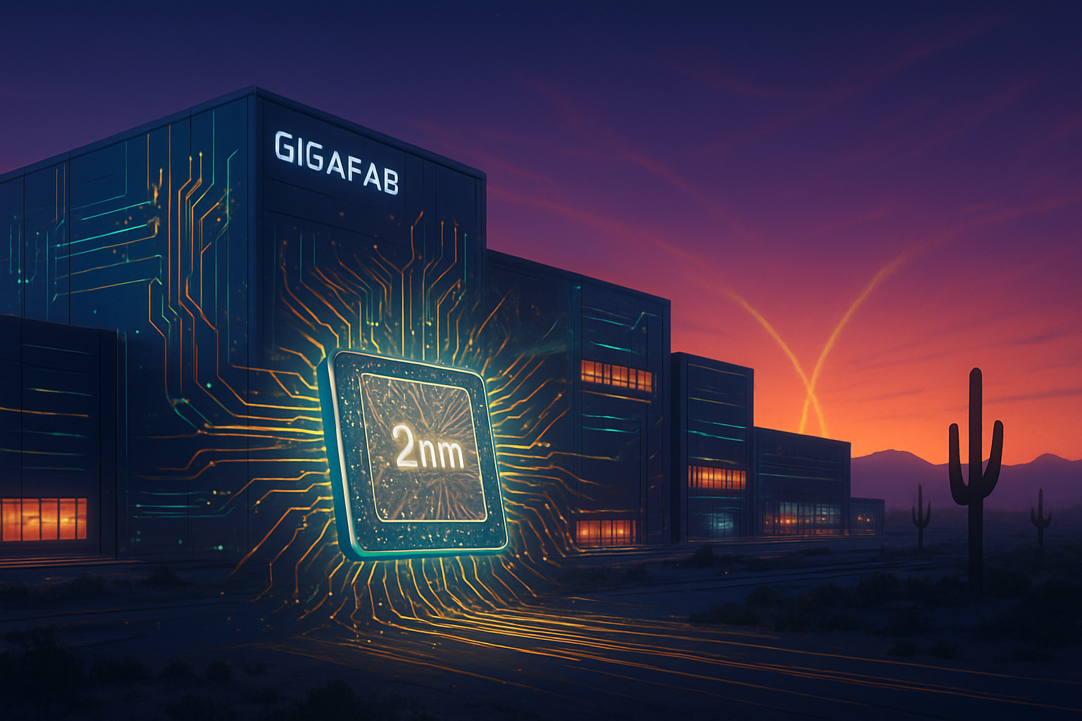
    As of December 24, 2025, the desert landscape of Phoenix, Arizona, has officially transformed into a cornerstone of the global semiconductor industry. Taiwan Semiconductor Manufacturing Company (NYSE:TSM), the world’s leading foundry, has announced a series of milestones at its "Fab 21" site that have silenced critics and reshaped the geopolitical map of high-tech manufacturing. Most notably, the facility's Phase 1 has reached full volume production for 4nm and 5nm nodes, achieving a staggering 92% yield—a figure that remarkably surpasses the yields of TSMC’s comparable facilities in Taiwan by nearly 4%.

    The immediate significance of this development cannot be overstated. For the first time, the United States is home to a facility capable of producing the world’s most advanced artificial intelligence and consumer electronics processors at a scale and efficiency that matches, or even exceeds, Asian counterparts. With the installation of 3nm equipment now underway and a clear roadmap toward 2nm volume production by late 2027, the "Arizona Gigafab" is no longer a theoretical project; it is an active, high-performance engine driving the next generation of AI innovation.

    Technical Milestones: From 4nm Mastery to the 3nm Horizon

    The technical achievements at Fab 21 represent a masterclass in technology transfer and precision engineering. Phase 1 is currently churning out 4nm (N4P) wafers for industry giants, utilizing advanced Extreme Ultraviolet (EUV) lithography to pack billions of transistors onto silicon. The reported 92% yield rate is a critical technical victory, proving that the highly complex chemical and mechanical processes required for sub-7nm manufacturing can be successfully replicated in the U.S. workforce environment. This success is attributed to a mix of automated precision systems and a rigorous training program that saw thousands of American engineers embedded in TSMC’s Tainan facilities over the past two years.

    As Phase 1 reaches its stride, Phase 2 is entering the "cleanroom preparation" stage. This involves the installation of hyper-clean HVAC systems and specialized chemical delivery networks designed to support the 3nm (N3) process. Unlike the 5nm and 4nm nodes, the 3nm process offers a 15% speed improvement at the same power or a 30% power reduction at the same speed. The "tool-in" phase for the 3nm line, which includes the latest generation of EUV machines from ASML (NASDAQ:ASML), is slated for early 2026, with mass production pulled forward to 2027 due to overwhelming customer demand.

    Looking further ahead, TSMC officially broke ground on Phase 3 in April 2025. This facility is being built specifically for the 2nm (N2) node, which will mark a historic transition from the traditional FinFET transistor architecture to Gate-All-Around (GAA) nanosheet technology. This architectural shift is essential for maintaining Moore’s Law, as it allows for better electrostatic control and lower leakage as transistors shrink to near-atomic scales. By the time Phase 3 is operational in late 2027, Arizona will be at the absolute bleeding edge of physics-defying semiconductor design.

    The Power Players: Apple, Nvidia, and the localized Supply Chain

    The primary beneficiaries of this expansion are the "Big Three" of the silicon world: Apple (NASDAQ:AAPL), NVIDIA (NASDAQ:NVDA), and AMD (NASDAQ:AMD). Apple has already secured the lion's share of Phase 1 capacity, using the Arizona-made 4nm chips for its latest A-series and M-series processors. For Apple, having a domestic source for its flagship silicon mitigates the risk of Pacific supply chain disruptions and aligns with its strategic goal of increasing U.S.-based manufacturing.

    NVIDIA and AMD are equally invested, particularly as the demand for AI training hardware remains insatiable. NVIDIA’s Blackwell AI GPUs are now being fabricated in Phoenix, providing a critical buffer for the data center market. While silicon fabrication was the first step, a 2025 partnership with Amkor (NASDAQ:AMKR) has begun to localize advanced packaging services in Arizona as well. This means that for the first time, a chip can be designed, fabricated, and packaged within a 50-mile radius in the United States, drastically reducing the "wafer-to-market" timeline and strengthening the competitive advantage of American fabless companies.

    This localized ecosystem creates a "virtuous cycle" for startups and smaller AI labs. As the heavyweights anchor the facility, the surrounding infrastructure—including specialized chemical suppliers and logistics providers—becomes more robust. This lowers the barrier to entry for smaller firms looking to secure domestic capacity for custom AI accelerators, potentially disrupting the current market where only the largest companies can afford the logistical hurdles of overseas manufacturing.

    Geopolitics and the New Semiconductor Landscape

    The progress in Arizona is a crowning achievement for the U.S. CHIPS and Science Act. The finalized agreement in late 2024, which provided TSMC with $6.6 billion in direct grants and $5 billion in loans, has proven to be a catalyst for broader investment. TSMC has since increased its total commitment to the Arizona site to a staggering $165 billion, planning a total of six fabs. This massive capital injection signals a shift in the global AI landscape, where "silicon sovereignty" is becoming as important as energy independence.

    The success of the Arizona site also changes the narrative regarding the "Taiwan Risk." While Taiwan remains the undisputed heart of TSMC’s operations, the Arizona Gigafab provides a vital "hot spare" for the world’s most critical technology. Industry experts have noted that the 92% yield rate in Phoenix effectively debunked the myth that high-end semiconductor manufacturing is culturally or geographically tethered to East Asia. This milestone serves as a blueprint for other nations—such as Germany and Japan—where TSMC is also expanding, suggesting a more decentralized and resilient global chip supply.

    However, this expansion is not without its concerns. The sheer scale of the Phoenix operations has placed immense pressure on local water resources and the energy grid. While TSMC has implemented world-leading water reclamation technologies, the environmental impact of a six-fab complex in a desert remains a point of contention and a challenge for local policymakers. Furthermore, the "N-2" policy—where Taiwan-based fabs must remain two generations ahead of overseas sites—ensures that while Arizona is cutting-edge, the absolute pinnacle of research and development remains in Hsinchu.

    The Road to 2027: 2nm and the A16 Node

    The roadmap for the next 24 months is clear but ambitious. Following the 3nm equipment installation in 2026, the industry will be watching for the first "pilot runs" of 2nm silicon in late 2027. The 2nm node is expected to be the workhorse for the next generation of AI models, providing the efficiency needed for edge-AI devices—like glasses and wearables—to perform complex reasoning without tethering to the cloud.

    Beyond 2nm, TSMC has already hinted at the "A16" node (1.6nm), which will introduce backside power delivery. This technology moves the power wiring to the back of the wafer, freeing up space on the front for more signal routing and denser transistor placement. Experts predict that if the current construction pace holds, Arizona could see A16 production as early as 2028 or 2029, effectively turning the desert into the most advanced square mile of real estate on the planet.

    The primary challenge moving forward will be the talent pipeline. While the yield rates are high, the demand for specialized technicians and EUV operators is expected to triple as Phase 2 and Phase 3 come online. TSMC, along with partners like Intel (NASDAQ:INTC), which is also expanding in Arizona, will need to continue investing heavily in local university programs and vocational training to sustain this growth.

    A New Era for American Silicon

    TSMC’s progress in Arizona marks a definitive turning point in the history of technology. The transition from a construction site to a high-yield, high-volume 4nm manufacturing hub—with 3nm and 2nm nodes on the immediate horizon—represents the successful "re-shoring" of the world’s most complex industrial process. It is a validation of the CHIPS Act and a testament to the collaborative potential of global tech leaders.

    As we look toward 2026, the focus will shift from "can they build it?" to "how fast can they scale it?" The installation of 3nm equipment in the coming months will be the next major benchmark to watch. For the AI industry, this means more chips, higher efficiency, and a more secure supply chain. For the world, it means that the brains of our most advanced machines are now being forged in the heart of the American Southwest.


    This content is intended for informational purposes only and represents analysis of current AI developments.

    TokenRing AI delivers enterprise-grade solutions for multi-agent AI workflow orchestration, AI-powered development tools, and seamless remote collaboration platforms.
    For more information, visit https://www.tokenring.ai/.

  • TSMC Arizona’s 3nm Acceleration: Bringing Advanced Manufacturing to US Soil

    TSMC Arizona’s 3nm Acceleration: Bringing Advanced Manufacturing to US Soil

    As of December 23, 2025, the landscape of global semiconductor manufacturing has reached a pivotal turning point. Taiwan Semiconductor Manufacturing Company (NYSE: TSM), the world’s leading contract chipmaker, has officially accelerated its roadmap for its sprawling Fab 21 complex in Phoenix, Arizona. With Phase 1 already churning out high volumes of 4nm and 5nm silicon, the company has confirmed that early equipment installation and cleanroom preparation for Phase 2—the facility’s 3nm production line—are well underway. This development marks a significant victory for the U.S. strategy to repatriate critical technology infrastructure and secure the supply chain for the next generation of artificial intelligence.

    The acceleration of the Arizona site, which was once plagued by labor disputes and construction delays, signals a newfound confidence in the American "Silicon Desert." By pulling forward the timeline for 3nm production to 2027—a full year ahead of previous estimates—TSMC is responding to insatiable demand from domestic tech giants who are eager to insulate their AI hardware from geopolitical volatility in the Pacific.

    Technical Milestones and the 92% Yield Breakthrough

    The technical prowess displayed at Fab 21 has silenced many early skeptics of U.S.-based advanced manufacturing. In a milestone report released late this year, TSMC (NYSE: TSM) revealed that its Arizona Phase 1 facility has achieved a 4nm yield rate of 92%. Remarkably, this figure is approximately four percentage points higher than the yields achieved at equivalent facilities in Taiwan. This success is attributed to the implementation of "Digital Twin" manufacturing technology, where a virtual model of the fab allows engineers to simulate and optimize processes in real-time before they are executed on the physical floor.

    The transition to 3nm (N3) technology in Phase 2 represents a massive leap in transistor density and energy efficiency. The 3nm process is expected to offer up to a 15% speed improvement at the same power level or a 30% power reduction at the same speed compared to the 5nm node. As of December 2025, the physical shell of the Phase 2 fab is complete, and the installation of internal infrastructure—including hyper-cleanroom HVAC systems and specialized chemical delivery networks—is progressing rapidly. The primary "tool-in" phase, involving the move-in of multi-million dollar Extreme Ultraviolet (EUV) lithography machines, is now slated for early 2026, setting the stage for volume production in 2027.

    A Windfall for AI Giants and the End-to-End Supply Chain

    The acceleration of 3nm capabilities in Arizona is a strategic boon for the primary architects of the AI revolution. Apple (NASDAQ: AAPL), NVIDIA (NASDAQ: NVDA), and AMD (NASDAQ: AMD) have already secured the lion's share of the capacity at Fab 21. For NVIDIA, the ability to produce its high-end Blackwell AI processors on U.S. soil reduces the logistical and political risks associated with shipping wafers across the Taiwan Strait. While the front-end wafers are currently the focus, the recent groundbreaking of a $7 billion advanced packaging facility by Amkor Technology (NASDAQ: AMKR) in nearby Peoria, Arizona, is the final piece of the puzzle.

    By 2027, the partnership between TSMC and Amkor will enable a "100% American-made" lifecycle for AI chips. Historically, even chips fabricated in the U.S. had to be sent to Taiwan for Chip-on-Wafer-on-Substrate (CoWoS) packaging. The emergence of a domestic packaging ecosystem ensures that companies like NVIDIA and AMD can maintain a resilient, end-to-end supply chain within North America. This shift not only provides a competitive advantage in terms of lead times but also allows these firms to market their products as "sovereign-secure" to government and enterprise clients.

    The Geopolitical Significance of the Silicon Desert

    The strategic importance of TSMC’s Arizona expansion cannot be overstated. It serves as the crown jewel of the U.S. CHIPS and Science Act, which provided TSMC with $6.6 billion in direct grants and up to $5 billion in loans. As of late 2025, the U.S. Department of Commerce has finalized several tranches of this funding, citing TSMC's ability to meet and exceed its technical milestones. This development places the U.S. in a much stronger position relative to global competitors, including Samsung (KRX: 005930) and Intel (NASDAQ: INTC), both of which are racing to bring their own advanced nodes to market.

    This move toward "geographic decoupling" is a direct response to the heightened tensions in the South China Sea. By establishing a "GigaFab" cluster in Arizona—now projected to include a total of six fabs with a total investment of $165 billion—TSMC is creating a high-security alternative to its Taiwan-based operations. This has fundamentally altered the global semiconductor landscape, moving the center of gravity for high-end manufacturing closer to the software and design hubs of Silicon Valley.

    Looking Ahead: The Road to 2nm and Beyond

    The roadmap for TSMC Arizona does not stop at 3nm. In April 2025, the company broke ground on Phase 3 (Fab 3), which is designated for the even more advanced 2nm (N2) and A16 (1.6nm) angstrom-class process nodes. These technologies will be essential for the next generation of AI models, which will require exponential increases in computational power and efficiency. Experts predict that by 2030, the Arizona complex will be capable of producing the most advanced semiconductors in the world, potentially reaching parity with TSMC’s flagship "Fab 18" in Tainan.

    However, challenges remain. The industry continues to grapple with a shortage of specialized talent required to operate these highly automated facilities. While the 92% yield rate suggests that the initial workforce hurdles have been largely overcome, the scale of the expansion—from two fabs to six—will require a massive influx of engineers and technicians over the next five years. Furthermore, the integration of advanced packaging on-site will require a new level of coordination between TSMC and its ecosystem partners.

    Conclusion: A New Era for American Silicon

    The status of TSMC’s Fab 21 in December 2025 represents a landmark achievement in industrial policy and technological execution. The acceleration of 3nm equipment installation and the surprising yield success of Phase 1 have transformed the "Silicon Desert" from a theoretical ambition into a tangible reality. For the U.S., this facility is more than just a factory; it is a critical safeguard for the future of artificial intelligence and national security.

    As we move into 2026, the industry will be watching closely for the arrival of the first EUV tools in Phase 2 and the continued progress of the Phase 3 groundbreaking. With the support of the CHIPS Act and the commitment of the world's largest tech companies, TSMC Arizona has set a new standard for global semiconductor manufacturing, ensuring that the most advanced chips of the future will bear the "Made in USA" label.


    This content is intended for informational purposes only and represents analysis of current AI developments.

    TokenRing AI delivers enterprise-grade solutions for multi-agent AI workflow orchestration, AI-powered development tools, and seamless remote collaboration platforms.
    For more information, visit https://www.tokenring.ai/.