Tag: ASIC

  • The Bespoke Billion: How Broadcom Is Architecting the Post-Nvidia AI Era Through Custom Silicon and Light

    The Bespoke Billion: How Broadcom Is Architecting the Post-Nvidia AI Era Through Custom Silicon and Light

    As of February 6, 2026, the artificial intelligence landscape is witnessing a monumental shift in power. While the initial wave of the AI revolution was defined by general-purpose GPUs, the current era belongs to "bespoke compute." Broadcom Inc. (NASDAQ: AVGO) has emerged as the primary architect of this new world, solidifying its leadership in custom AI Application-Specific Integrated Circuits (ASICs) and revolutionary silicon photonics. Analysts across Wall Street have responded with a wave of "Overweight" ratings, signaling that Broadcom’s role as the indispensable backbone of the hyperscale data center is no longer a projection—it is a reality.

    The significance of Broadcom’s ascent lies in its ability to help the world’s largest tech companies bypass the high costs and supply constraints of general-purpose chips. By delivering specialized accelerators (XPUs) tailored to specific AI models, Broadcom is enabling a transition toward more efficient, cost-effective, and scalable infrastructure. With AI-related revenue projected to reach nearly $50 billion this year, the company is no longer just a networking player; it is the central engine for the custom-built AI future.

    At the heart of Broadcom’s technical dominance is the shipping of the Tomahawk 6 series, the world’s first 102.4 Terabits per second (Tbps) switching silicon. Announced in late 2025 and seeing massive volume deployment in early 2026, the Tomahawk 6 doubles the bandwidth of its predecessor, facilitating the interconnection of million-node XPU clusters. Unlike previous generations, the Tomahawk 6 is built specifically for the "Scale-Out" requirements of Generative AI, utilizing 200G SerDes (Serializer/Deserializer) technology to handle the unprecedented data throughput required for training trillion-parameter models.

    Broadcom is also pioneering the use of Co-Packaged Optics (CPO) through its "Davisson" platform. In traditional data centers, electrical signals are converted to light using pluggable transceivers at the edge of the switch. Broadcom’s CPO technology integrates the optical engines directly onto the ASIC package, reducing power consumption by 3.5x and lowering the cost per bit by 40%. This breakthrough addresses the "power wall"—the physical limit of how much electricity a data center can consume—by eliminating energy-intensive copper components. Furthermore, the newly released Jericho 4 router chip introduces "Cognitive Routing," a feature that uses hardware-level intelligence to manage congestion and prevent "packet stalls," which can otherwise derail multi-week AI training jobs.

    This technological leap has major implications for tech giants like Google (NASDAQ: GOOGL), Meta (NASDAQ: META), and OpenAI. Analysts from firms like Wells Fargo and Bank of America note that Broadcom is the primary beneficiary of the "Nvidia tax" avoidance strategy. Hyperscalers are increasingly moving away from Nvidia (NASDAQ: NVDA) proprietary stacks in favor of custom XPUs. For instance, Broadcom is the lead partner for Google’s TPU v7 and Meta’s MTIA v4. These custom chips are optimized for the companies' specific workloads—such as Llama-4 or Gemini—offering performance-per-watt metrics that general-purpose GPUs cannot match.

    The market positioning is further bolstered by a landmark partnership with OpenAI. Broadcom is reportedly providing the silicon architecture for OpenAI’s massive 10-gigawatt data center initiative, an endeavor estimated to have a lifetime value exceeding $100 billion. By providing a vertically integrated solution that includes the compute ASIC, the high-speed Ethernet NIC (Thor Ultra), and the back-end switching fabric, Broadcom offers a "turnkey" custom silicon service. This puts pressure on traditional chipmakers and provides a strategic advantage to AI labs that want to control their own hardware destiny without the overhead of building an entire chip division from scratch.

    Broadcom’s success reflects a broader trend in the AI industry: the triumph of open standards over proprietary ecosystems. While Nvidia’s InfiniBand was once the gold standard for AI networking, the industry has shifted back toward Ethernet, largely due to Broadcom’s innovations. The Ultra Ethernet Consortium (UEC), of which Broadcom is a founding member, has standardized the protocols that allow Ethernet to match or exceed InfiniBand’s latency and reliability. This shift ensures that the AI infrastructure of the future remains interoperable, preventing any single vendor from maintaining a permanent monopoly on the data center fabric.

    However, this transition is not without concerns. The extreme concentration of Broadcom’s revenue among a handful of hyperscale customers—Google, Meta, and OpenAI—creates a dependency that analysts watch closely. Furthermore, as AI models become more specialized, the "bespoke" nature of these chips means they lack the versatility of GPUs. If the industry were to pivot toward a fundamentally different neural architecture, custom ASICs could face faster obsolescence. Despite these risks, the current trajectory suggests that the efficiency gains of custom silicon are too significant for the world's largest compute spenders to ignore.

    Looking ahead to the remainder of 2026 and into 2027, Broadcom is already laying the groundwork for Gen 4 Co-Packaged Optics. This next generation aims to achieve 400G per lane capability, effectively doubling networking speeds again within the next 24 months. Experts predict that as the industry moves toward 200-terabit switches, the integration of silicon photonics will move from a competitive advantage to a mandatory requirement. We also expect to see "edge-to-cloud" custom silicon initiatives, where Broadcom-designed chips power both the massive training clusters in the cloud and the localized inference engines in high-end consumer devices.

    The next major milestone to watch will be the full-scale deployment of "optical interconnects" between individual XPUs, effectively turning a whole data center rack into a single, giant, light-speed computer. While challenges remain in the yield and manufacturing complexity of these advanced packages, Broadcom’s partnership with leading foundries suggests they are on track to overcome these hurdles. The goal is clear: to reach a point where networking and compute are indistinguishable, linked by a seamless fabric of silicon and light.

    In summary, Broadcom has successfully transformed itself from a diversified component supplier into the vital architect of the AI infrastructure era. By dominating the two most critical bottlenecks in AI—bespoke compute and high-speed networking—the company has secured a massive backlog of orders that analysts believe will drive $100 billion in AI revenue by 2027. The move to an "Overweight" rating by major financial institutions is a recognition that Broadcom’s silicon photonics and ASIC leadership provide a "moat" that is becoming increasingly difficult for competitors to cross.

    As we move further into 2026, the industry should watch for the first real-world performance benchmarks of the OpenAI custom clusters and the broader adoption of the Tomahawk 6. These milestones will likely confirm whether the shift toward custom, Ethernet-based AI fabrics is the permanent blueprint for the next decade of computing. For now, Broadcom stands as the quiet giant of the AI revolution, proving that in the race for artificial intelligence, the one who controls the flow of data—and the light that carries it—ultimately wins.


    This content is intended for informational purposes only and represents analysis of current AI developments.

    TokenRing AI delivers enterprise-grade solutions for multi-agent AI workflow orchestration, AI-powered development tools, and seamless remote collaboration platforms.
    For more information, visit https://www.tokenring.ai/.

  • The Bespoke Silicon Revolution: Broadcom’s $50 Billion Surge Redefines the AI Hardware Landscape

    The Bespoke Silicon Revolution: Broadcom’s $50 Billion Surge Redefines the AI Hardware Landscape

    As of early 2026, the artificial intelligence industry has reached a critical inflection point where generic hardware is no longer enough to satisfy the hunger of multi-trillion parameter models. Leading this fundamental shift is Broadcom Inc. (NASDAQ: AVGO), which has successfully transitioned from a diversified networking giant into the primary architect of the custom AI silicon era. By positioning itself as the indispensable partner for hyperscalers like Google and Meta, and now the primary engine behind OpenAI’s hardware ambitions, Broadcom is witnessing a historic surge in revenue that is reshaping the semiconductor market.

    The numbers tell a story of rapid, unprecedented dominance. After closing a blockbuster fiscal year 2025 with $20 billion in AI-related revenue, Broadcom is now on track to more than double that figure in 2026, with projections soaring toward the $50 billion mark. With an AI order backlog currently sitting at a staggering $73 billion, the company has effectively bifurcated the AI chip market: while Nvidia Corp. (NASDAQ: NVDA) remains the king of general-purpose training, Broadcom has become the undisputed sovereign of custom Application-Specific Integrated Circuits (ASICs), providing the "bespoke compute" that allows the world’s largest tech companies to bypass the "Nvidia tax" and build more efficient, specialized data centers.

    Engineering the Architecture of Sovereign AI

    The core of Broadcom’s technical advantage lies in its ability to co-design chips that strip away the silicon "cruft" found in general-purpose GPUs. While Nvidia’s Blackwell and newly released Rubin platforms must support a vast array of legacy applications and diverse workloads, Broadcom’s ASICs—such as Google’s (NASDAQ: GOOGL) TPU v7 and Meta Platforms' (NASDAQ: META) MTIA v4—are laser-focused on the specific mathematical operations required for Large Language Models (LLMs). This specialization allows for a 30% to 50% improvement in performance-per-watt compared to off-the-shelf GPUs. In an era where data center power limits have become the primary bottleneck for AI scaling, this energy efficiency is not just a cost-saving measure; it is a strategic necessity.

    The technical specifications of these new accelerators are formidable. The Google TPU v7 (codenamed "Ironwood"), built on a 3nm process, is optimized specifically for the latest Gemini 2.0 and 3.0 models. Meanwhile, the Meta MTIA v4 (Santa Barbara), currently deploying across Meta’s massive fleet of servers, features liquid-cooled rack integration and advanced 3D Torus networking topologies. This architecture allows companies to cluster over 9,000 chips into a single unified "Superpod" with minimal latency, far exceeding the scale of traditional GPU clusters. Broadcom provides the critical intellectual property—including high-speed SerDes, HBM controllers, and networking interconnects—while leveraging its deep partnership with Taiwan Semiconductor Manufacturing Co. (NYSE: TSM) for advanced packaging.

    Shifting the Competitive Power Balance

    This surge in custom silicon is fundamentally altering the power dynamics among tech giants. By developing their own chips through Broadcom, companies like Meta and Google are achieving a level of vertical integration that provides a significant competitive moat. For these hyperscalers, the shift to ASICs represents a "decoupling" from the supply chain volatility and high margins associated with third-party GPU vendors. It allows them to optimize their entire stack—from the underlying silicon and networking to the AI models themselves—resulting in a lower Total Cost of Ownership (TCO) that startups and smaller labs simply cannot match.

    The market is also witnessing the emergence of a "second tier" of custom silicon providers, most notably Marvell Technology Inc. (NASDAQ: MRVL), which has secured its own landmark deals with Amazon and Microsoft. However, Broadcom remains the dominant force, controlling roughly 65% of the custom AI ASIC market. This positioning has made Broadcom a "proxy" for the overall health of the AI infrastructure sector. As OpenAI officially joins Broadcom’s customer roster with a multi-billion dollar project to build its own "sovereignty" chip, the company’s role has evolved from a supplier to a strategic kingmaker. OpenAI’s move to internal silicon, specifically designed to run its high-intensity "reasoning" models like the o1-series, signals that the industry's heaviest hitters are no longer content with being customers—they want to be architects.

    The Broader Implications for the AI Landscape

    Broadcom’s success reflects a broader trend toward the fragmentation of the AI hardware landscape. We are moving away from a world of "one size fits all" compute and toward a heterogeneous environment where different chips are tuned for specific tasks: training, inference, or reasoning. This shift mimics the evolution of the mobile industry, where Apple’s move to internal silicon eventually redefined the performance benchmarks for the entire smartphone market. By enabling Google, Meta, and OpenAI to do the same for AI, Broadcom is accelerating a future where the most advanced AI capabilities are tied directly to proprietary hardware.

    However, this trend toward custom silicon also raises concerns about market consolidation. As the barrier to entry for high-end AI moves from "buying GPUs" to "designing multi-billion dollar custom chips," the gap between the "Big Five" hyperscalers and the rest of the industry may become an unbridgeable chasm. Furthermore, the reliance on a few key players—specifically Broadcom for design and TSMC for fabrication—creates new points of failure in the global AI supply chain. The environmental impact is also a double-edged sword; while ASICs are more efficient per operation, the sheer scale of the new data centers being built to house them is driving global energy demand to unprecedented heights.

    The Horizon: 2nm Nodes and Reasoning-Specific Silicon

    Looking toward 2027 and beyond, the roadmap for custom silicon is focused on the transition to 2nm-class nodes and the integration of even more advanced "Chip-on-Wafer-on-Substrate" (CoWoS) packaging. Broadcom is already in the early stages of development for the TPU v8, which is expected to begin mass production in the second half of 2026. These next-generation chips will likely incorporate on-chip optical interconnects, further reducing the latency and energy costs associated with moving data between processors and memory—a critical requirement for the next generation of "Agentic AI" that must process information in real-time.

    Experts predict that the next major frontier will be the development of silicon specifically optimized for "reasoning-heavy" inference. Current chips are largely designed for the "next-token prediction" paradigm of GPT-4. However, as models move toward more complex chain-of-thought processing, the demand for chips with significantly higher local memory bandwidth and specialized logic for logic-gate simulation will grow. Broadcom’s partnership with OpenAI is widely believed to be the first major step in this direction, potentially creating a new category of "Reasoning Units" that differ fundamentally from current NPUs and GPUs.

    Conclusion: A Legacy Defined by Customization

    Broadcom’s transformation into an AI silicon powerhouse is one of the most significant developments in the history of the semiconductor industry. By 2026, the company has proven that the path to AI supremacy is paved with customization, not just raw power. Its $50 billion revenue surge is a testament to the fact that for the world’s most advanced AI labs, the "off-the-shelf" era is effectively over. Broadcom’s ability to turn the complex requirements of companies like Google, Meta, and OpenAI into physical, high-performance silicon has placed it at the center of the AI ecosystem.

    In the coming months, the industry will be watching closely as the first "live silicon" from the OpenAI-Broadcom partnership begins to ship. This event will likely serve as a litmus test for whether internal silicon can truly provide the "sovereignty" that AI labs crave. For investors and technologists alike, Broadcom is no longer just a networking company; it is the master builder of the infrastructure that will define the next decade of artificial intelligence.


    This content is intended for informational purposes only and represents analysis of current AI developments.

    TokenRing AI delivers enterprise-grade solutions for multi-agent AI workflow orchestration, AI-powered development tools, and seamless remote collaboration platforms.
    For more information, visit https://www.tokenring.ai/.

  • Broadcom’s Custom AI Silicon Boom: Beyond the Google TPU

    Broadcom’s Custom AI Silicon Boom: Beyond the Google TPU

    As of early 2026, the artificial intelligence landscape is witnessing a seismic shift in how the world’s most powerful models are powered. While the industry spent years in the shadow of general-purpose GPUs, a new era of "bespoke compute" has arrived, spearheaded by Broadcom Inc. (NASDAQ: AVGO). Once synonymous primarily with Google’s (NASDAQ: GOOGL) Tensor Processing Units (TPUs), Broadcom has successfully diversified its custom AI Application-Specific Integrated Circuit (ASIC) business into a multi-customer powerhouse, securing landmark deals with Meta (NASDAQ: META), OpenAI, and Anthropic.

    This transition marks a pivotal moment in the "Compute Wars." By co-designing specialized silicon and high-speed networking fabrics, Broadcom is enabling hyperscalers to break free from the supply constraints and high premiums associated with off-the-shelf hardware. With AI-related revenue projected to hit a staggering $46 billion in 2026—a 134% year-over-year increase—Broadcom has effectively positioned itself as the structural architect of the next generation of AI infrastructure.

    The Technical Edge: TPU v7, MTIA v4, and the 1.6T Networking Revolution

    The technical foundation of Broadcom’s dominance lies in its ability to integrate high-performance compute with industry-leading networking. In late 2025, Broadcom and Google debuted the TPU v7 (Ironwood), a 3nm marvel designed specifically for large-scale inference and reasoning. Featuring 192GB of HBM3e memory and a massive 9.6 Tbps Inter-Chip Interconnect (ICI) bandwidth, Ironwood is optimized for the multi-trillion parameter models that define the current AGI-frontier. Similarly, the partnership with Meta has moved into its next phase with the MTIA v4 (Santa Barbara), which introduces liquid-cooled rack integration to handle the unprecedented thermal demands of 180kW+ AI clusters.

    Perhaps most significant is Broadcom’s advancements in networking, which serve as the "connective tissue" for these custom chips. The Tomahawk 6 (TH6) switch ASIC, shipping in volume as of early 2026, is the world’s first 102.4 Tbps switch, enabling the transition to 1.6T Ethernet. This allows for the creation of clusters containing over one million XPUs (accelerated processing units) with minimal latency. By championing the Ethernet for Scale-Up Networking (ESUN) workstream, Broadcom is providing a viable, open-standard alternative to NVIDIA’s (NASDAQ: NVDA) proprietary NVLink, allowing customers to build "scale-up" fabrics within the rack using standard Ethernet protocols.

    Industry experts note that this "end-to-end" approach—where the AI chip and the network switch are co-designed—solves the "IO bottleneck" that has long plagued large-scale AI training. Initial reactions from the research community suggest that Broadcom’s custom silicon-plus-Ethernet strategy provides up to 50% better throughput for distributed training tasks compared to traditional InfiniBand-based setups.

    Reducing the "NVIDIA Tax" and Empowering the Hyperscale Elite

    The strategic implications of Broadcom’s custom silicon boom are profound. For years, the "NVIDIA tax"—the high margin paid for H100 and Blackwell GPUs—was the cost of doing business in AI. However, companies like Meta and Google have realized that at their scale, even a 10% efficiency gain in silicon can save billions in capital expenditure and energy costs. By partnering with Broadcom, these giants gain total control over the instruction set architecture (ISA), memory configurations, and power envelopes of their hardware, tailoring them specifically to their proprietary algorithms.

    The recent entry of OpenAI and Anthropic into Broadcom’s custom silicon stable has sent shockwaves through the industry. OpenAI’s landmark collaboration to co-develop custom accelerators for its 10-gigawatt data center projects signifies a long-term pivot toward hardware sovereignty. Anthropic, similarly, has committed to a $10 billion+ deal for custom silicon, aiming to optimize its Claude models on hardware that prioritizes safety-aligned "constitutional AI" features at the silicon level. This shift significantly dilutes NVIDIA’s market dominance, as the most valuable AI workloads move from general-purpose GPUs to specialized ASICs.

    For Broadcom, this diversification creates a "structural moat." Unlike competitors who may offer only the chip or only the switch, Broadcom’s portfolio includes the SerDes, the HBM controllers, the optical interconnects, and the networking silicon. This vertical integration makes them the indispensable partner for any company large enough to design its own chip but too small to manage the entire semiconductor manufacturing and networking stack alone.

    A New Global Standard: The Rise of Sovereign AI Compute

    Broadcom’s success fits into a broader trend of "Sovereign AI," where both corporations and nations seek to control their own compute destiny. The move toward custom ASICs is not just about cost; it is about performance ceilings. As LLMs evolve into "Large World Models" that incorporate video, audio, and real-time physical simulation, the data movement requirements are exceeding what general-purpose hardware can provide. Broadcom’s introduction of the Jericho4 ASIC, which enables Data Center Interconnects (DCI) across distances of up to 100km with lossless performance, is a direct response to the power and space constraints of single-site mega-datacenters.

    There are, however, concerns regarding the concentration of power. With Broadcom holding a nearly 60% market share in the custom AI ASIC space, the industry has effectively traded one gatekeeper (NVIDIA) for another. Furthermore, the reliance on high-end 3nm and 2nm manufacturing nodes at TSMC (NYSE: TSM) remains a potential geopolitical bottleneck. Despite these concerns, the shift to custom silicon is viewed as a necessary evolution for the industry to reach the next milestone in AI capability without collapsing the global energy grid.

    The Horizon: 2nm Processes and Co-Packaged Optics

    Looking ahead to 2027 and beyond, Broadcom is already laying the groundwork for the next jump in performance. The transition to 2nm process technology is expected to yield another 30% improvement in energy efficiency, a critical metric as AI power consumption becomes a global regulatory concern. Furthermore, the adoption of Co-Packaged Optics (CPO) will likely become the standard for 3.2T and 6.4T networking, replacing traditional copper and pluggable transceivers with silicon photonics integrated directly onto the chip package.

    Predictive models suggest that by late 2026, the majority of "Frontier Model" training will occur on custom ASICs rather than general-purpose GPUs. We may also see Broadcom expand its "silicon-as-a-service" model, potentially offering modular chiplet designs that allow smaller tech companies to "mix and match" Broadcom’s networking IP with their own proprietary logic.

    Conclusion: Broadcom's Indispensable Role in the AI Era

    Broadcom’s transformation from a diversified semiconductor firm into the primary architect of the world’s AI infrastructure is one of the most significant business stories of the mid-2020s. By moving "beyond the Google TPU" and securing the top tier of AI labs—Meta, OpenAI, and Anthropic—Broadcom has proven that the future of AI is bespoke. Its dual-threat mastery of both custom compute and high-speed Ethernet networking has created a feedback loop that will be difficult for any competitor, even NVIDIA, to break.

    As we move through 2026, the key developments to watch will be the first live silicon deployments from the OpenAI-Broadcom partnership and the industry-wide adoption of 1.6T Ethernet. Broadcom is no longer just a component supplier; it is the platform upon which the age of AGI is being built.


    This content is intended for informational purposes only and represents analysis of current AI developments.

    TokenRing AI delivers enterprise-grade solutions for multi-agent AI workflow orchestration, AI-powered development tools, and seamless remote collaboration platforms.
    For more information, visit https://www.tokenring.ai/.

  • Silicon Sovereignty: The Great Decoupling as Custom AI Chips Reshape the Cloud

    Silicon Sovereignty: The Great Decoupling as Custom AI Chips Reshape the Cloud

    MENLO PARK, CA — As of January 12, 2026, the artificial intelligence industry has reached a pivotal inflection point. For years, the story of AI was synonymous with the meteoric rise of one company’s hardware. However, the dawn of 2026 marks the definitive end of the general-purpose GPU monopoly. In a coordinated yet competitive surge, the world’s largest cloud providers—Alphabet Inc. (NASDAQ: GOOGL), Amazon.com, Inc. (NASDAQ: AMZN), and Microsoft Corp. (NASDAQ: MSFT)—have successfully transitioned a massive portion of their internal and customer-facing workloads to proprietary custom silicon.

    This shift toward Application-Specific Integrated Circuits (ASICs) represents more than just a cost-saving measure; it is a strategic decoupling from the supply chain volatility and "NVIDIA tax" that defined the early 2020s. With the arrival of Google’s TPU v7 "Ironwood," Amazon’s 3nm Trainium3, and Microsoft’s Maia 200, the "Big Three" are no longer just software giants—they have become some of the world’s most sophisticated semiconductor designers, fundamentally altering the economics of intelligence.

    The 3nm Frontier: Technical Mastery in the ASIC Age

    The technical gap between general-purpose GPUs and custom ASICs has narrowed to the point of vanishing, particularly in the realm of power efficiency and specific model architectures. Leading the charge is Google’s TPU v7 (Ironwood), which entered mass deployment this month. Built on a dual-chiplet architecture to maximize manufacturing yields, Ironwood delivers a staggering 4,614 teraflops of FP8 performance. More importantly, it features 192GB of HBM3e memory with 7.4 TB/s of bandwidth, specifically tuned for the massive context windows of Gemini 2.5. Unlike traditional setups, Google utilizes its proprietary Optical Circuit Switching (OCS), allowing up to 9,216 chips to be interconnected in a single "superpod" with near-zero latency and significantly lower power draw than electrical switching.

    Amazon’s Trainium3, unveiled at the tail end of 2025, has become the first AI chip to hit the 3nm process node in high-volume production. Developed in partnership with Alchip and utilizing HBM3e from SK Hynix (KRX: 000660), Trainium3 offers a 2x performance leap over its predecessor. Its standout feature is the NeuronLink v3 interconnect, which allows for seamless "UltraServer" configurations. AWS has strategically prioritized air-cooled designs for Trainium3, allowing it to be deployed in legacy data centers where liquid-cooling retrofits for NVIDIA Corp. (NASDAQ: NVDA) chips would be prohibitively expensive.

    Microsoft’s Maia 200 (Braga), despite early design pivots, is now in full-scale production. Built on TSMC’s N3E process, the Maia 200 is less about raw training power and more about the "Inference Flip"—the industry's move toward optimizing the cost of running models like GPT-5 and the "o1" reasoning series. Microsoft has integrated the Microscaling (MX) data format into the silicon, which drastically reduces memory footprint and power consumption during the complex chain-of-thought processing required by modern agentic AI.

    The Inference Flip and the New Market Order

    The competitive implications of this silicon surge are profound. While NVIDIA still commands approximately 80-85% of the total AI accelerator revenue, the sub-market for inference—the actual running of AI models—has seen a dramatic shift. By early 2026, over two-thirds of all AI compute spending is dedicated to inference rather than training. In this high-margin territory, custom ASICs have captured nearly 30% of cloud-allocated workloads. For the hyperscalers, the strategic advantage is clear: vertical integration allows them to offer AI services at 30-50% lower costs than competitors relying solely on merchant silicon.

    This development has forced a reaction from the broader industry. Broadcom Inc. (NASDAQ: AVGO) has emerged as the silent kingmaker of this era, co-designing the TPU with Google and the MTIA with Meta Platforms, Inc. (NASDAQ: META). Meanwhile, Marvell Technology, Inc. (NASDAQ: MRVL) continues to dominate the optical interconnect and custom CPU space for Amazon. Even smaller players like MediaTek are entering the fray, securing contracts for "Lite" versions of these chips, such as the TPU v7e, signaling a diversification of the supply chain that was unthinkable two years ago.

    NVIDIA has not remained static. At CES 2026, the company officially launched its Vera Rubin architecture, featuring the Rubin GPU and the Vera CPU. By moving to a strict one-year release cycle, NVIDIA hopes to stay ahead of the ASICs through sheer performance density and the continued entrenchment of its CUDA software ecosystem. However, with the maturation of OpenXLA and OpenAI’s Triton—which now provides a "lingua franca" for writing kernels across different hardware—the "software moat" that once protected GPUs is beginning to show cracks.

    Silicon Sovereignty and the Global AI Landscape

    Beyond the balance sheets of Big Tech, the rise of custom silicon is a cornerstone of the "Silicon Sovereignty" movement. In 2026, national security is increasingly defined by a country's ability to secure domestic AI compute. We are seeing a shift away from globalized supply chains toward regionalized "AI Stacks." Japan’s Rapidus and various EU-funded initiatives are now following the hyperscaler blueprint, designing bespoke chips to ensure they are not beholden to foreign entities for their foundational AI infrastructure.

    The environmental impact of this shift is equally significant. General-purpose GPUs are notoriously power-hungry, often requiring upwards of 1kW per chip. In contrast, the purpose-built nature of the TPU v7 and Trainium3 allows for 40-70% better energy efficiency per token generated. As global regulators tighten carbon reporting requirements for data centers, the "performance-per-watt" metric has become as important as raw FLOPS. The ability of ASICs to do more with less energy is no longer just a technical feat—it is a regulatory necessity.

    This era also marks a departure from the "one-size-fits-all" model of AI. In 2024, every problem was solved with a massive LLM on a GPU. In 2026, we see a fragmented landscape: specialized chips for vision, specialized chips for reasoning, and specialized chips for edge-based agentic workflows. This specialization is democratizing high-performance AI, allowing startups to rent specific "ASIC-optimized" instances on Azure or AWS that are tailored to their specific model architecture, rather than overpaying for general-purpose compute they don't fully utilize.

    The Horizon: 2nm and Optical Computing

    Looking ahead to the remainder of 2026 and into 2027, the roadmap for custom silicon is moving toward the 2nm process node. Both Google and Amazon have already reserved significant capacity at TSMC for 2027, signaling that the ASIC war is only in its opening chapters. The next major hurdle is the full integration of optical computing—moving data via light not just between racks, but directly onto the chip package itself to eliminate the "memory wall" that currently limits AI scaling.

    Experts predict that the next generation of chips, such as the rumored TPU v8 and Maia 300, will feature HBM4 memory, which promises to double the bandwidth again. The challenge, however, remains the software. While tools like Triton and JAX have made ASICs more accessible, the long-tail of AI developers still finds the NVIDIA ecosystem more "turn-key." The company that can truly bridge the gap between custom hardware performance and developer ease-of-use will likely dominate the second half of the decade.

    A New Era of Hardware-Defined AI

    The rise of custom AI silicon represents the most significant shift in computing architecture since the transition from mainframes to client-server models. By taking control of the silicon, Google, Amazon, and Microsoft have insulated themselves from the volatility of the merchant chip market and paved the way for a more efficient, cost-effective AI future. The "Great Decoupling" from NVIDIA is not a sign of the GPU giant's failure, but rather a testament to the sheer scale that AI compute has reached—it is now a utility too vital to be left to a single provider.

    As we move further into 2026, the industry should watch for the first "ASIC-native" models—AI architectures designed from the ground up to exploit the specific systolic array structures of the TPU or the unique memory hierarchy of Trainium. When the hardware begins to dictate the shape of the intelligence it runs, the era of truly hardware-defined AI will have arrived.


    This content is intended for informational purposes only and represents analysis of current AI developments.

    TokenRing AI delivers enterprise-grade solutions for multi-agent AI workflow orchestration, AI-powered development tools, and seamless remote collaboration platforms.
    For more information, visit https://www.tokenring.ai/.

  • The Silicon Sovereignty Era: Hyperscalers Break NVIDIA’s Grip with 3nm Custom AI Chips

    The Silicon Sovereignty Era: Hyperscalers Break NVIDIA’s Grip with 3nm Custom AI Chips

    The dawn of 2026 has brought a seismic shift to the artificial intelligence landscape, as the world’s largest cloud providers—the hyperscalers—have officially transitioned from being NVIDIA’s (NASDAQ: NVDA) biggest customers to its most formidable architectural rivals. For years, the industry operated under a "one-size-fits-all" GPU paradigm, but a new surge in custom Application-Specific Integrated Circuits (ASICs) has shattered that consensus. Driven by the relentless demand for more efficient inference and the staggering costs of frontier model training, Google, Amazon, and Meta have unleashed a new generation of 3nm silicon that is fundamentally rewriting the economics of AI.

    At the heart of this revolution is a move toward vertical integration that rivals the early days of the mainframe. By designing their own chips, these tech giants are no longer just buying compute; they are engineering it to fit the specific contours of their proprietary models. This strategic pivot is delivering 30% to 40% better price-performance for internal workloads, effectively commoditizing high-end AI compute and providing a critical buffer against the supply chain bottlenecks and premium margins that have defined the NVIDIA era.

    The 3nm Power Play: Ironwood, Trainium3, and the Scaling of MTIA

    The technical specifications of this new silicon class are nothing short of breathtaking. Leading the charge is Google, a subsidiary of Alphabet Inc. (NASDAQ: GOOGL), with its TPU v7p (Ironwood). Built on Taiwan Semiconductor Manufacturing Company’s (NYSE: TSM) cutting-edge 3nm (N3P) process, Ironwood is a dual-chiplet powerhouse featuring a massive 192GB of HBM3E memory. With a memory bandwidth of 7.4 TB/s and a peak performance of 4.6 PFLOPS of dense FP8 compute, the TPU v7p is designed specifically for the "age of inference," where massive context windows and complex reasoning are the new standard. Google has already moved into mass deployment, reporting that over 75% of its Gemini model computations are now handled by its internal TPU fleet.

    Not to be outdone, Amazon.com, Inc. (NASDAQ: AMZN) has officially ramped up production of AWS Trainium3. Also utilizing the 3nm process, Trainium3 packs 144GB of HBM3E and delivers 2.52 PFLOPS of FP8 performance per chip. What sets the AWS offering apart is its "UltraServer" configuration, which interconnects 144 chips into a single, liquid-cooled rack capable of matching NVIDIA’s Blackwell architecture in rack-level performance while offering a significantly more efficient power profile. Meanwhile, Meta Platforms, Inc. (NASDAQ: META) is scaling its Meta Training and Inference Accelerator (MTIA). While its current v2 "Artemis" chips focus on offloading recommendation engines from GPUs, Meta’s 2026 roadmap includes its first dedicated in-house training chip, designed to support the development of Llama 4 and beyond within its massive "Titan" data center clusters.

    These advancements represent a departure from the general-purpose nature of the GPU. While an NVIDIA H100 or B200 is designed to be excellent at almost any parallel task, these custom ASICs are "leaner." By stripping away legacy components and focusing on specific data formats like MXFP8 and MXFP4, and optimizing for specific software frameworks like PyTorch (for Meta) or JAX (for Google), these chips achieve higher throughput per watt. The integration of advanced liquid cooling and proprietary interconnects like Google’s Optical Circuit Switching (OCS) allows these chips to operate in unified domains of nearly 10,000 units, creating a level of "cluster-scale" efficiency that was previously unattainable.

    Disrupting the Monopoly: Market Implications for the GPU Giants

    The immediate beneficiaries of this silicon surge are the hyperscalers themselves, who can now offer AI services at a fraction of the cost of their competitors. AWS has already begun using Trainium3 as a "bargaining chip," implementing price cuts of up to 45% on its NVIDIA-based instances to remain competitive with its own internal hardware. This internal competition is a nightmare scenario for NVIDIA’s margins. While the AI pioneer still dominates the high-end training market, the shift toward inference—projected to account for 70% of all AI workloads in 2026—plays directly into the hands of custom ASIC designers who can optimize for the specific latency and throughput requirements of a deployed model.

    The ripple effects extend to the "enablers" of this custom silicon wave: Broadcom Inc. (NASDAQ: AVGO) and Marvell Technology, Inc. (NASDAQ: MRVL). Broadcom has emerged as the undisputed leader in the custom ASIC space, acting as the primary design partner for Google’s TPUs and Meta’s MTIA. Analysts project Broadcom’s AI semiconductor revenue will hit a staggering $46 billion in 2026, driven by a $73 billion backlog of orders from hyperscalers and firms like Anthropic. Marvell, meanwhile, has secured its place by partnering with AWS on Trainium and Microsoft Corporation (NASDAQ: MSFT) on its Maia accelerators. These design firms provide the critical IP blocks—such as high-speed SerDes and memory controllers—that allow cloud giants to bring chips to market in record time.

    For the broader tech industry, this development signals a fracturing of the AI hardware market. Startups and mid-sized enterprises that were once priced out of the NVIDIA ecosystem are finding a new home in "capacity blocks" of custom silicon. By commoditizing the underlying compute, the hyperscalers are shifting the competitive focus away from who has the most GPUs and toward who has the best data and the most efficient model architectures. This "Silicon Sovereignty" allows the likes of Google and Meta to insulate themselves from the "NVIDIA Tax," ensuring that their massive capital expenditures translate more directly into shareholder value rather than flowing into the coffers of a single hardware vendor.

    A New Architectural Paradigm: Beyond the GPU

    The surge of custom silicon is more than just a cost-saving measure; it is a fundamental shift in the AI landscape. We are moving away from a world where software was written to fit the hardware, and into an era of "hardware-software co-design." When Meta develops a chip in tandem with the PyTorch framework, or Google optimizes its TPU for the Gemini architecture, they achieve a level of vertical integration that mirrors Apple’s success with its M-series silicon. This trend suggests that the "one-size-fits-all" approach of the general-purpose GPU may eventually be relegated to the research lab, while production-scale AI is handled by highly specialized, purpose-built machines.

    However, this transition is not without its concerns. The rise of proprietary silicon could lead to a "walled garden" effect in AI development. If a model is trained and optimized specifically for Google’s TPU v7p, moving that workload to AWS or an on-premise NVIDIA cluster becomes a non-trivial engineering challenge. There are also environmental implications; while these chips are more efficient per token, the sheer scale of deployment is driving unprecedented energy demands. The "Titan" clusters Meta is building in 2026 are gigawatt-scale projects, raising questions about the long-term sustainability of the AI arms race and the strain it puts on national power grids.

    Comparing this to previous milestones, the 2026 silicon surge feels like the transition from CPU-based mining to ASICs in the early days of Bitcoin—but on a global, industrial scale. The era of experimentation is over, and the era of industrial-strength, optimized production has begun. The breakthroughs of 2023 and 2024 were about what AI could do; the breakthroughs of 2026 are about how AI can be delivered to billions of people at a sustainable cost.

    The Horizon: What Comes After 3nm?

    Looking ahead, the roadmap for custom silicon shows no signs of slowing down. As we move toward 2nm and beyond, the focus is expected to shift from raw compute power to "advanced packaging" and "photonic interconnects." Marvell and Broadcom are already experimenting with 3.5D packaging and optical I/O, which would allow chips to communicate at the speed of light, effectively turning an entire data center into a single, giant processor. This would solve the "memory wall" that currently limits the size of the models we can train.

    In the near term, expect to see these custom chips move deeper into the "edge." While 2026 is the year of the data center ASIC, 2027 and 2028 will likely see these same architectures scaled down for use in "AI PCs" and autonomous vehicles. The challenges remain significant—particularly in the realm of software compilers that can automatically optimize code for diverse hardware targets—but the momentum is undeniable. Experts predict that by the end of the decade, over 60% of all AI compute will run on non-NVIDIA hardware, a total reversal of the market dynamics we saw just three years ago.

    Closing the Loop on Custom Silicon

    The mass deployment of Google’s TPU v7p, AWS’s Trainium3, and Meta’s MTIA marks the definitive end of the GPU’s undisputed reign. By taking control of their silicon destiny, the hyperscalers have not only reduced their reliance on a single vendor but have also unlocked a new level of performance that will enable the next generation of "Agentic AI" and trillion-parameter reasoning models. The 30-40% price-performance advantage of these ASICs is the new baseline for the industry, forcing every player in the ecosystem to innovate or be left behind.

    As we move through 2026, the key metrics to watch will be the "utilization rates" of these custom clusters and the speed at which third-party developers adopt the proprietary software stacks required to run on them. The "Silicon Sovereignty" era is here, and it is defined by a simple truth: in the age of AI, the most powerful software is only as good as the silicon it was born to run on. The battle for the future of intelligence is no longer just being fought in the cloud—it’s being fought in the transistor.


    This content is intended for informational purposes only and represents analysis of current AI developments.

    TokenRing AI delivers enterprise-grade solutions for multi-agent AI workflow orchestration, AI-powered development tools, and seamless remote collaboration platforms.
    For more information, visit https://www.tokenring.ai/.

  • NVIDIA Blackwell Ships Amid the Rise of Custom Hyperscale Silicon

    NVIDIA Blackwell Ships Amid the Rise of Custom Hyperscale Silicon

    As of December 24, 2025, the artificial intelligence landscape has reached a pivotal juncture marked by the massive global rollout of NVIDIA’s (NASDAQ: NVDA) Blackwell B200 GPUs. While NVIDIA continues to post record-breaking quarterly revenues—recently hitting a staggering $57 billion—the architecture’s arrival coincides with a strategic rebellion from its largest customers. Cloud hyperscalers like Google (NASDAQ: GOOGL), Amazon (NASDAQ: AMZN), and Microsoft (NASDAQ: MSFT) are no longer content with being mere distributors of NVIDIA hardware; they are now aggressively deploying their own custom AI ASICs to reclaim control over their soaring operational costs.

    The shipment of Blackwell represents the culmination of a year-long effort to overcome initial design hurdles and supply chain bottlenecks. However, the market NVIDIA enters in late 2025 is far more fragmented than the one dominated by its predecessor, the H100. As inference demand begins to outpace training requirements, the industry is witnessing a "Great Decoupling," where the raw, unbridled power of NVIDIA’s silicon is being weighed against the specialized efficiency and lower total cost of ownership (TCO) offered by custom-built hyperscale silicon.

    The Technical Powerhouse: Blackwell’s Dual-Die Dominance

    The Blackwell B200 is a technical marvel that redefines the limits of semiconductor engineering. Moving away from the single-die approach of the Hopper architecture, Blackwell utilizes a dual-die chiplet design fused by a blistering 10 TB/s interconnect. This configuration packs 208 billion transistors and provides 192GB of HBM3e memory, manufactured on TSMC’s (NYSE: TSM) advanced 4NP process. The most significant technical leap, however, is the introduction of the Second-Gen Transformer Engine and FP4 precision. This allows the B200 to deliver up to 18 PetaFLOPS of inference performance—a nearly 30x increase in throughput for trillion-parameter models compared to the H100 when deployed in liquid-cooled NVL72 rack configurations.

    Initial reactions from the AI research community have been a mix of awe and logistical concern. While labs like OpenAI and Anthropic have praised the B200’s ability to handle the massive memory requirements of "reasoning" models (such as the o1 series), data center operators are grappling with the immense power demands. A single Blackwell rack can consume over 120kW, requiring a wholesale transition to liquid-cooling infrastructure. This thermal density has created a high barrier to entry, effectively favoring large-scale providers who can afford the specialized facilities needed to run Blackwell at peak performance. Despite these challenges, NVIDIA’s software ecosystem, centered around CUDA, remains a formidable moat that continues to make Blackwell the "gold standard" for frontier model training.

    The Hyperscale Counter-Offensive: Custom Silicon Ascendant

    While NVIDIA’s hardware is shipping in record volumes—estimated at 1,000 racks per week—the tech giants are increasingly pivoting to their own internal solutions. Google has recently unveiled its TPU v7 (Ironwood), built on a 3nm process, which aims to match Blackwell’s raw compute while offering superior energy efficiency for Google’s internal services like Search and Gemini. Similarly, Amazon Web Services (AWS) launched Trainium 3 at its recent re:Invent conference, claiming a 4.4x performance boost over its predecessor. These custom chips are not just for internal use; AWS and Google are offering deep discounts—up to 70%—to startups that choose their proprietary silicon over NVIDIA instances, a move designed to erode NVIDIA’s market share in the high-volume inference sector.

    This shift has profound implications for the competitive landscape. Microsoft, despite facing delays with its Maia 200 (Braga) chip, has pivoted toward a "system-level" optimization strategy, integrating its Azure Cobalt 200 CPUs to maximize the efficiency of its existing hardware clusters. For AI startups, this diversification is a boon. By becoming platform-agnostic, companies like Anthropic are now training and deploying models across a heterogeneous mix of NVIDIA GPUs, Google TPUs, and AWS Trainium. This strategy mitigates the "NVIDIA Tax" and shields these companies from the supply chain volatility that characterized the 2023-2024 AI boom.

    A Shifting Global Landscape: Sovereign AI and the Inference Pivot

    Beyond the battle between NVIDIA and the hyperscalers, a new demand engine has emerged: Sovereign AI. Nations such as Japan, Saudi Arabia, and the United Arab Emirates are investing billions to build domestic compute stacks. In Japan, the government-backed Rapidus is racing to produce 2nm logic chips, while Saudi Arabia’s Vision 2030 initiative is leveraging subsidized energy to undercut Western data center costs by 30%. These nations are increasingly looking for alternatives to the U.S.-centric supply chain, creating a permanent new class of buyers that are just as likely to invest in custom local silicon as they are in NVIDIA’s flagship products.

    This geopolitical shift is occurring alongside a fundamental change in the AI workload mix. In late 2025, the industry is moving from a "training-heavy" phase to an "inference-heavy" phase. While training a frontier model still requires the massive parallel processing power of a Blackwell cluster, running those models at scale for millions of users demands cost-efficiency above all else. This is where custom ASICs (Application-Specific Integrated Circuits) shine. By stripping away the general-purpose features of a GPU that aren't needed for inference, hyperscalers can deliver AI services at a fraction of the power and cost, challenging NVIDIA’s dominance in the most profitable segment of the market.

    The Road to Rubin: NVIDIA’s Next Leap

    NVIDIA is not standing still in the face of this rising competition. To maintain its lead, the company has accelerated its roadmap to a one-year cadence, recently teasing the "Rubin" architecture slated for 2026. Rubin is expected to leapfrog current custom silicon by moving to a 3nm process and incorporating HBM4 memory, which will double memory channels and address the primary bottleneck for next-generation reasoning models. The Rubin platform will also feature the new Vera CPU, creating a tightly integrated "Vera Rubin" ecosystem that will be difficult for competitors to unbundle.

    Experts predict that the next two years will see a bifurcated market. NVIDIA will likely retain a 90% share of the "Frontier Training" market, where the most advanced models are built. However, the "Commodity Inference" market—where models are actually put to work—will become a battlefield for custom silicon. The challenge for NVIDIA will be to prove that its system-level integration (including NVLink and InfiniBand networking) provides enough value to justify its premium price tag over the "good enough" performance of custom hyperscale chips.

    Summary of a New Era in AI Compute

    The shipping of NVIDIA Blackwell marks the end of the "GPU shortage" era and the beginning of the "Silicon Diversity" era. Key takeaways from this development include the successful deployment of chiplet-based AI hardware at scale, the rise of 3nm custom ASICs as legitimate competitors for inference workloads, and the emergence of Sovereign AI as a major market force. While NVIDIA remains the undisputed king of performance, the aggressive moves by Google, Amazon, and Microsoft suggest that the era of a single-vendor monoculture is coming to an end.

    In the coming months, the industry will be watching the real-world performance of Trainium 3 and the eventual launch of Microsoft’s Maia 200. As these custom chips reach parity with NVIDIA for specific tasks, the focus will shift from raw FLOPS to energy efficiency and software accessibility. For now, Blackwell is the most powerful tool ever built for AI, but for the first time, it is no longer the only game in town. The "Great Decoupling" has begun, and the winners will be those who can most effectively balance the peak performance of NVIDIA with the specialized efficiency of custom silicon.


    This content is intended for informational purposes only and represents analysis of current AI developments.

    TokenRing AI delivers enterprise-grade solutions for multi-agent AI workflow orchestration, AI-powered development tools, and seamless remote collaboration platforms.
    For more information, visit https://www.tokenring.ai/.

  • The Decentralized Brain: Specialized AI Chips Drive Real-Time Intelligence to the Edge

    The Decentralized Brain: Specialized AI Chips Drive Real-Time Intelligence to the Edge

    The landscape of artificial intelligence is undergoing a profound transformation, moving beyond the confines of centralized cloud data centers to the very periphery of networks. This paradigm shift, driven by the synergistic interplay of AI and edge computing, is manifesting in the rapid development of specialized semiconductor chips. These innovative processors are meticulously engineered to bring AI processing closer to the data source, enabling real-time AI applications that promise to redefine industries from autonomous vehicles to personalized healthcare. This evolution in hardware is not merely an incremental improvement but a fundamental re-architecting of how AI is deployed, making it more ubiquitous, efficient, and responsive.

    The immediate significance of this trend in semiconductor development is the enablement of truly intelligent edge devices. By performing AI computations locally, these chips dramatically reduce latency, conserve bandwidth, enhance privacy, and ensure reliability even in environments with limited or no internet connectivity. This is crucial for time-sensitive applications where milliseconds matter, fostering a new age in predictive analysis and operational performance across a broad spectrum of industries.

    The Silicon Revolution: Technical Deep Dive into Edge AI Accelerators

    The technical advancements driving Edge AI are characterized by a diverse range of architectures and increasing capabilities, all aimed at optimizing AI workloads under strict power and resource constraints. Unlike general-purpose CPUs or even traditional GPUs, these specialized chips are purpose-built for the unique demands of neural networks.

    At the heart of this revolution are Neural Processing Units (NPUs) and Application-Specific Integrated Circuits (ASICs). NPUs, such as those found in Intel's (NASDAQ: INTC) Core Ultra processors and Arm's Ethos-U55, are designed for highly parallel neural network computations, excelling at tasks like image recognition and natural language processing. They often support low-bitwidth operations (INT4, INT8, FP8, FP16) for superior energy efficiency. Google's (NASDAQ: GOOGL) Edge TPU, an ASIC, delivers impressive tera-operations per second (TOPS) of INT8 performance at minimal power consumption, a testament to the efficiency of specialized design. Startups like Hailo and SiMa.ai are pushing boundaries, with Hailo-8 achieving up to 26 TOPS at around 2.5W (10 TOPS/W efficiency) and SiMa.ai's MLSoC delivering 50 TOPS at roughly 5W, with a second generation optimized for transformer architectures and Large Language Models (LLMs) like Llama2-7B.

    This approach significantly differs from previous cloud-centric models where raw data was sent to distant data centers for processing. Edge AI chips bypass this round-trip delay, enabling real-time responses critical for autonomous systems. Furthermore, they address the "memory wall" bottleneck through innovative memory architectures like In-Memory Computing (IMC), which integrates compute functions directly into memory, drastically reducing data movement and improving energy efficiency. The AI research community and industry experts have largely embraced these developments with excitement, recognizing the transformative potential to enable new services while acknowledging challenges like balancing accuracy with resource constraints and ensuring robust security on distributed devices. NVIDIA's (NASDAQ: NVDA) chief scientist, Bill Dally, has even noted that AI is "already performing parts of the design process better than humans" in chip design, indicating AI's self-reinforcing role in hardware innovation.

    Corporate Chessboard: Impact on Tech Giants, AI Labs, and Startups

    The rise of Edge AI semiconductors is fundamentally reshaping the competitive landscape, creating both immense opportunities and strategic imperatives for companies across the tech spectrum.

    Tech giants like Google (NASDAQ: GOOGL), Amazon (NASDAQ: AMZN), and Microsoft (NASDAQ: MSFT) are heavily investing in developing their own custom AI chips, such as ASICs and TPUs. This strategy provides them with strategic independence from third-party suppliers, optimizes their massive cloud AI workloads, reduces operational costs, and allows them to offer differentiated AI services. NVIDIA (NASDAQ: NVDA), a long-standing leader in AI hardware with its powerful GPUs and Jetson platform, continues to benefit from the demand for high-performance edge AI, particularly in robotics and advanced computer vision, leveraging its strong CUDA software ecosystem. Intel (NASDAQ: INTC) is also a significant player, with its Movidius accelerators and new Core Ultra processors designed for edge AI.

    AI labs and major AI companies are compelled to diversify their hardware supply chains to reduce reliance on single-source suppliers and achieve greater efficiency and scalability for their AI models. The ability to run more complex models on resource-constrained edge devices opens up vast new application domains, from localized generative AI to sophisticated predictive analytics. This shift could disrupt traditional cloud AI service models for certain applications, as more processing moves on-device.

    Startups are finding niches by providing highly specialized chips for enterprise needs or innovative power delivery solutions. Companies like Hailo, SiMa.ai, Kinara Inc., and Axelera AI are examples of firms making significant investments in custom silicon for on-device AI. While facing high upfront development costs, these nimble players can carve out disruptive footholds by offering superior performance-per-watt or unique architectural advantages for specific edge AI workloads. Their success often hinges on strategic partnerships with larger companies or focused market penetration in emerging sectors. The lower cost and energy efficiency of advancements in inference ICs also make Edge AI solutions more accessible for smaller companies.

    A New Era of Intelligence: Wider Significance and Future Landscape

    The proliferation of Edge AI semiconductors signifies a crucial inflection point in the broader AI landscape. It represents a fundamental decentralization of intelligence, moving beyond the cloud to create a hybrid AI ecosystem where AI workloads can dynamically leverage the strengths of both centralized and distributed computing. This fits into broader trends like "Micro AI" for hyper-efficient models on tiny devices and "Federated Learning," where devices collaboratively train models without sharing raw data, enhancing privacy and reducing network load. The emergence of "AI PCs" with integrated NPUs also heralds a new era of personal computing with offline AI capabilities.

    The impacts are profound: significantly reduced latency enables real-time decision-making for critical applications like autonomous driving and industrial automation. Enhanced privacy and security are achieved by keeping sensitive data local, a vital consideration for healthcare and surveillance. Conserved bandwidth and lower operational costs stem from reduced reliance on continuous cloud communication. This distributed intelligence also ensures greater reliability, as edge devices can operate independently of cloud connectivity.

    However, concerns persist. Edge devices inherently face hardware limitations in terms of computational power, memory, and battery life, necessitating aggressive model optimization techniques that can sometimes impact accuracy. The complexity of building and managing vast edge networks, ensuring interoperability across diverse devices, and addressing unique security vulnerabilities (e.g., physical tampering) are ongoing challenges. Furthermore, the rapid evolution of AI models, especially LLMs, creates a "moving target" for chip designers who must hardwire support for future AI capabilities into silicon.

    Compared to previous AI milestones, such as the adoption of GPUs for accelerating deep learning in the late 2000s, Edge AI marks a further refinement towards even more tailored and specialized solutions. While GPUs democratized AI training, Edge AI is democratizing AI inference, making intelligence pervasive. This "AI supercycle" is distinct due to its intense focus on the industrialization and scaling of AI, driven by the increasing complexity of modern AI models and the imperative for real-time responsiveness.

    The Horizon of Intelligence: Future Developments and Predictions

    The future of Edge AI semiconductors promises an even more integrated and intelligent world, with both near-term refinements and long-term architectural shifts on the horizon.

    In the near term (1-3 years), expect continued advancements in specialized AI accelerators, with NPUs becoming ubiquitous in consumer devices, from smartphones to "AI PCs" (projected to make up 43% of all PC shipments by the end of 2025). The transition to advanced process nodes (3nm and 2nm) will deliver further power reductions and performance boosts. Innovations in In-Memory Computing (IMC) and Near-Memory Computing (NMC) will move closer to commercial deployment, fundamentally addressing memory bottlenecks and enhancing energy efficiency for data-intensive AI workloads. The focus will remain on achieving ever-greater performance within strict power and thermal budgets, leveraging materials like silicon carbide (SiC) and gallium nitride (GaN) for power management.

    Long-term developments (beyond 3 years) include more radical shifts. Neuromorphic computing, inspired by the human brain, promises exceptional energy efficiency and adaptive learning capabilities, proliferating in edge AI and IoT devices. Photonic AI chips, utilizing light for computation, could offer dramatically higher bandwidth and lower power consumption, potentially revolutionizing data centers and distributed AI. The vision of AI-designed and self-optimizing chips, where AI itself becomes an architect in semiconductor development, could lead to fully autonomous manufacturing and continuous refinement of chip fabrication. The nascent integration of quantum computing with AI also holds the potential to unlock problem-solving capabilities far beyond classical limits.

    Potential applications on the horizon are vast: truly autonomous vehicles, drones, and robotics making real-time, safety-critical decisions; industrial automation with predictive maintenance and adaptive AI control; smart cities with intelligent traffic management; and hyper-personalized experiences in smart homes, wearables, and healthcare. Challenges include the continuous battle against power consumption and thermal management, optimizing memory bandwidth, ensuring scalability across diverse devices, and managing the escalating costs of advanced R&D and manufacturing.

    Experts predict explosive market growth, with the global AI chip market projected to surpass $150 billion in 2025 and potentially reach $1.3 trillion by 2030. This will drive intense diversification and customization of AI chips, moving away from "one size fits all" solutions. AI will become the "backbone of innovation" within the semiconductor industry itself, optimizing chip design and manufacturing. Strategic partnerships between hardware manufacturers, AI software developers, and foundries will be critical to accelerating innovation and capturing market share.

    Wrapping Up: The Pervasive Future of AI

    The interplay of AI and edge computing in semiconductor development marks a pivotal moment in AI history. It signifies a profound shift towards a distributed, ubiquitous intelligence that promises to integrate AI seamlessly into nearly every device and system. The key takeaway is that specialized hardware, designed for power efficiency and real-time processing, is decentralizing AI, enabling capabilities that were once confined to the cloud to operate at the very source of data.

    This development's significance lies in its ability to unlock the next generation of AI applications, fostering highly intelligent and adaptive environments across sectors. The long-term impact will be a world where AI is not just a tool but an embedded, responsive intelligence that enhances daily life, drives industrial efficiency, and accelerates scientific discovery. This shift also holds the promise of more sustainable AI solutions, as local processing often consumes less energy than continuous cloud communication.

    In the coming weeks and months, watch for continued exponential market growth and intensified investment in specialized AI hardware. Keep an eye on new generations of custom silicon from major players like NVIDIA (NASDAQ: NVDA), AMD (NASDAQ: AMD), Google (NASDAQ: GOOGL), and Intel (NASDAQ: INTC), as well as groundbreaking innovations from startups in novel computing paradigms. The rollout of "AI PCs" will redefine personal computing, and advancements in advanced networking and interconnects will be crucial for distributed AI workloads. Finally, geopolitical factors concerning semiconductor supply chains will continue to heavily influence the global AI hardware market, making resilience in manufacturing and supply critical. The semiconductor industry isn't just adapting to AI; it's actively shaping its future, pushing the boundaries of what intelligent systems can achieve at the edge.


    This content is intended for informational purposes only and represents analysis of current AI developments.

    TokenRing AI delivers enterprise-grade solutions for multi-agent AI workflow orchestration, AI-powered development tools, and seamless remote collaboration platforms.
    For more information, visit https://www.tokenring.ai/.

  • Beyond the GPU: Specialized AI Chips Ignite a New Era of Innovation

    Beyond the GPU: Specialized AI Chips Ignite a New Era of Innovation

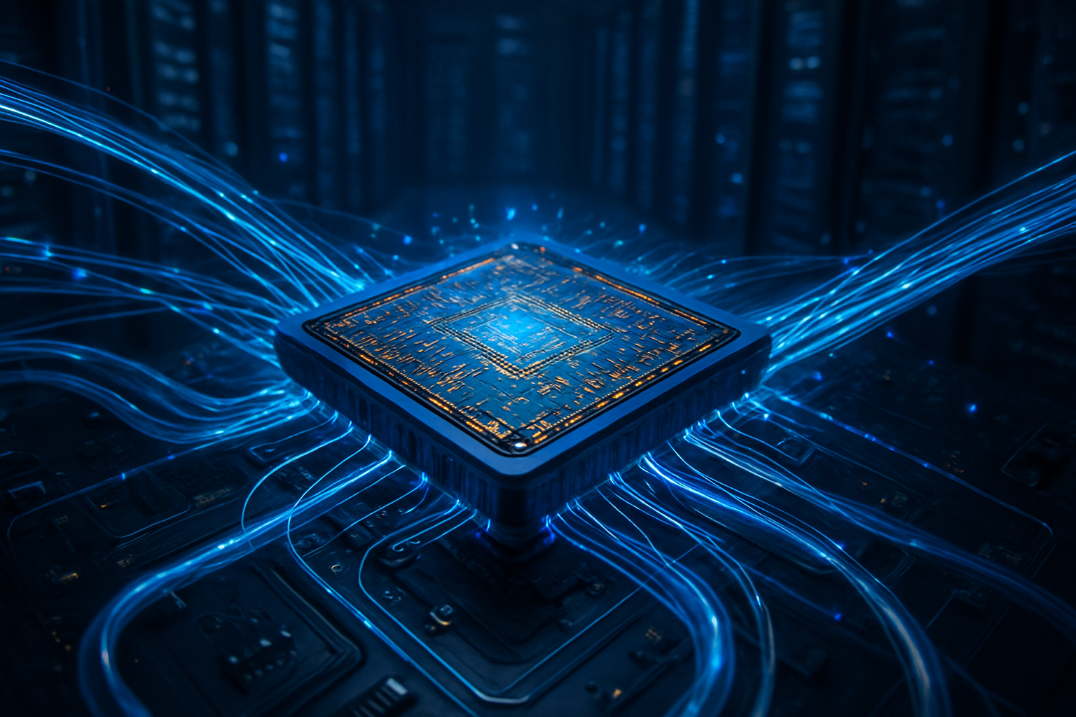
    The artificial intelligence landscape is currently experiencing a profound transformation, moving beyond the ubiquitous general-purpose GPUs and into a new frontier of highly specialized semiconductor chips. This strategic pivot, gaining significant momentum in late 2024 and projected to accelerate through 2025, is driven by the escalating computational demands of advanced AI models, particularly large language models (LLMs) and generative AI. These purpose-built processors promise unprecedented levels of efficiency, speed, and energy savings, marking a crucial evolution in AI hardware infrastructure.

    This shift signifies a critical response to the limitations of existing hardware, which, despite their power, are increasingly encountering bottlenecks in scalability and energy consumption as AI models grow exponentially in size and complexity. The emergence of Application-Specific Integrated Circuits (ASICs), neuromorphic chips, in-memory computing (IMC), and photonic processors is not merely an incremental upgrade but a fundamental re-architecture, tailored to unlock the next generation of AI capabilities.

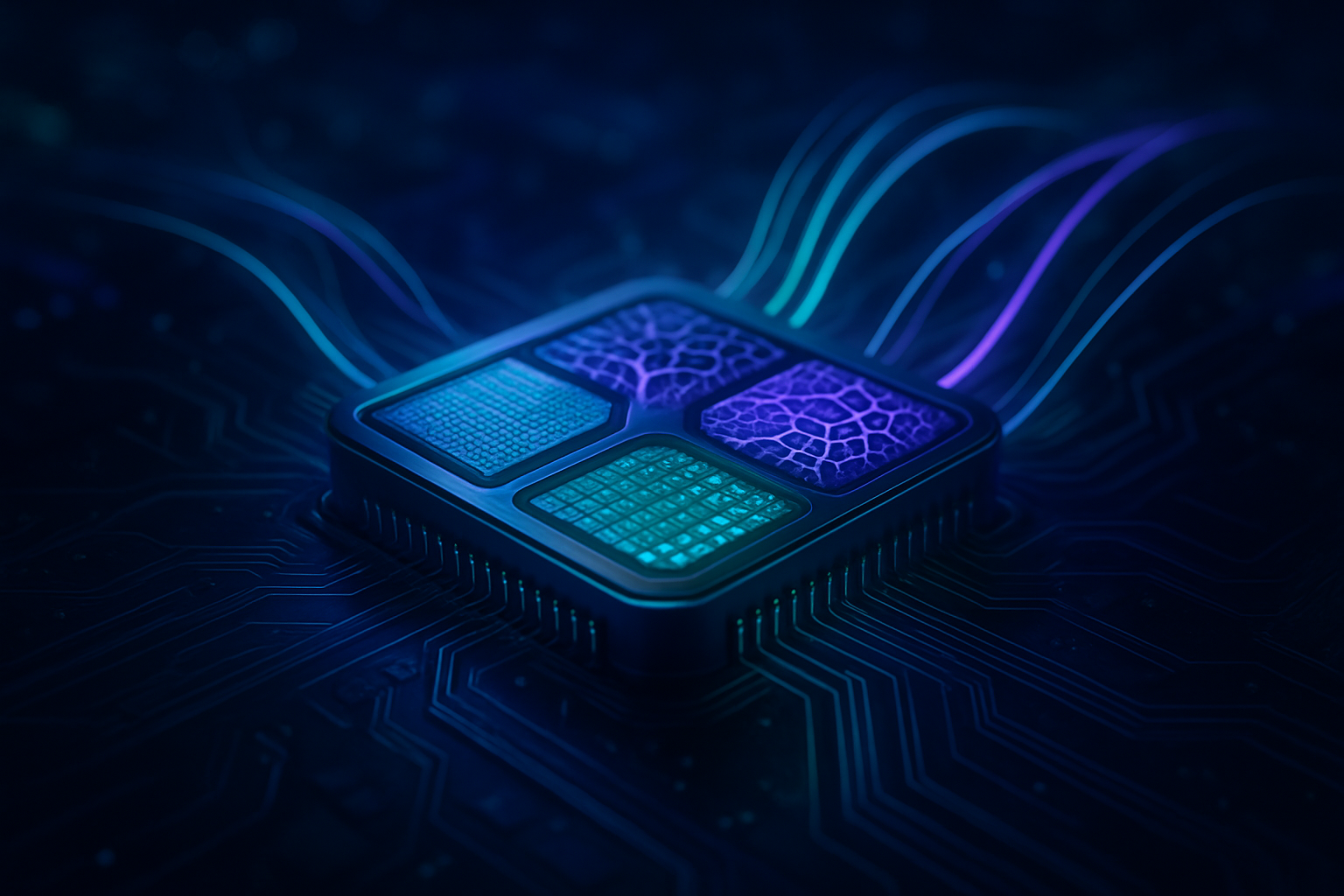
    The Architectural Revolution: Diving Deep into Specialized Silicon

    The technical advancements in specialized AI chips represent a diverse and innovative approach to AI computation, fundamentally differing from the parallel processing paradigms of general-purpose GPUs.

    Application-Specific Integrated Circuits (ASICs): These custom-designed chips are purpose-built for highly specific AI tasks, excelling in either accelerating model training or optimizing real-time inference. Unlike the versatile but less optimized nature of GPUs, ASICs are meticulously engineered for particular algorithms and data types, leading to significantly higher throughput, lower latency, and dramatically improved power efficiency for their intended function. Companies like OpenAI (in collaboration with Broadcom [NASDAQ: AVGO]), hyperscale cloud providers such as Amazon (NASDAQ: AMZN) with its Trainium and Inferentia chips, Google (NASDAQ: GOOGL) with its evolving TPUs and upcoming Trillium, and Microsoft (NASDAQ: MSFT) with Maia 100, are heavily investing in custom silicon. This specialization directly addresses the "memory wall" bottleneck that can limit the cost-effectiveness of GPUs in inference scenarios. The AI ASIC chip market, estimated at $15 billion in 2025, is projected for substantial growth.

    Neuromorphic Computing: This cutting-edge field focuses on designing chips that mimic the structure and function of the human brain's neural networks, employing "spiking neural networks" (SNNs). Key players include IBM (NYSE: IBM) with its TrueNorth, Intel (NASDAQ: INTC) with Loihi 2 (upgraded in 2024), and Brainchip Holdings Ltd. (ASX: BRN) with Akida. Neuromorphic chips operate in a massively parallel, event-driven manner, fundamentally different from traditional sequential processing. This enables ultra-low power consumption (up to 80% less energy) and real-time, adaptive learning capabilities directly on the chip, making them highly efficient for certain cognitive tasks and edge AI.

    In-Memory Computing (IMC): IMC chips integrate processing capabilities directly within the memory units, fundamentally addressing the "von Neumann bottleneck" where data transfer between separate processing and memory units consumes significant time and energy. By eliminating the need for constant data shuttling, IMC chips offer substantial improvements in speed, energy efficiency, and overall performance, especially for data-intensive AI workloads. Companies like Samsung (KRX: 005930) and SK Hynix (KRX: 000660) are demonstrating "processing-in-memory" (PIM) architectures within DRAMs, which can double the performance of traditional computing. The market for in-memory computing chips for AI is projected to reach $129.3 million by 2033, expanding at a CAGR of 47.2% from 2025.

    Photonic AI Chips: Leveraging light for computation and data transfer, photonic chips offer the potential for extremely high bandwidth and low power consumption, generating virtually no heat. They can encode information in wavelength, amplitude, and phase simultaneously, potentially making current GPUs obsolete. Startups like Lightmatter and Celestial AI are innovating in this space. Researchers from Tsinghua University in Beijing showcased a new photonic neural network chip named Taichi in April 2024, claiming it's 1,000 times more energy-efficient than NVIDIA's (NASDAQ: NVDA) H100.

    Initial reactions from the AI research community and industry experts are overwhelmingly positive, with significant investments and strategic shifts indicating a strong belief in the transformative potential of these specialized architectures. The drive for customization is seen as a necessary step to overcome the inherent limitations of general-purpose hardware for increasingly complex and diverse AI tasks.

    Reshaping the AI Industry: Corporate Battles and Strategic Plays

    The advent of specialized AI chips is creating profound competitive implications, reshaping the strategies of tech giants, AI labs, and nimble startups alike.

    Beneficiaries and Market Leaders: Hyperscale cloud providers like Google, Microsoft, and Amazon are among the biggest beneficiaries, using their custom ASICs (TPUs, Maia 100, Trainium/Inferentia) to optimize their cloud AI workloads, reduce operational costs, and offer differentiated AI services. Meta Platforms (NASDAQ: META) is also developing its custom Meta Training and Inference Accelerator (MTIA) processors for internal AI workloads. While NVIDIA (NASDAQ: NVDA) continues to dominate the GPU market, its new Blackwell platform is designed to maintain its lead in generative AI, but it faces intensified competition. AMD (NASDAQ: AMD) is aggressively pursuing market share with its Instinct MI series, notably the MI450, through strategic partnerships with companies like Oracle (NYSE: ORCL) and OpenAI. Startups like Groq (with LPUs optimized for inference), Tenstorrent, SambaNova Systems, and Hailo are also making significant strides, offering innovative solutions across various specialized niches.

    Competitive Implications: Major AI labs like OpenAI, Google DeepMind, and Anthropic are actively seeking to diversify their hardware supply chains and reduce reliance on single-source suppliers like NVIDIA. OpenAI's partnership with Broadcom for custom accelerator chips and deployment of AMD's MI450 chips with Oracle exemplify this strategy, aiming for greater efficiency and scalability. This competition is expected to drive down costs and foster accelerated innovation. For tech giants, developing custom silicon provides strategic independence, allowing them to tailor performance and cost for their unique, massive-scale AI workloads, thereby disrupting the traditional cloud AI services market.

    Disruption and Strategic Advantages: The shift towards specialized chips is disrupting existing products and services by enabling more efficient and powerful AI. Edge AI devices, from autonomous vehicles and industrial robotics to smart cameras and AI-enabled PCs (projected to make up 43% of all shipments by the end of 2025), are being transformed by low-power, high-efficiency NPUs. This enables real-time decision-making, enhanced privacy, and reduced reliance on cloud resources. The strategic advantages are clear: superior performance and speed, dramatic energy efficiency, improved cost-effectiveness at scale, and the unlocking of new capabilities for real-time applications. Hardware has re-emerged as a strategic differentiator, with companies leveraging specialized chips best positioned to lead in their respective markets.

    The Broader Canvas: AI's Future Forged in Silicon

    The emergence of specialized AI chips is not an isolated event but a critical component of a broader "AI supercycle" that is fundamentally reshaping the semiconductor industry and the entire technological landscape.

    Fitting into the AI Landscape: The overarching trend is a diversification and customization of AI chips, driven by the imperative for enhanced performance, greater energy efficiency, and the widespread enablement of edge computing. The global AI chip market, valued at $44.9 billion in 2024, is projected to reach $460.9 billion by 2034, growing at a CAGR of 27.6% from 2025 to 2034. ASICs are becoming crucial for inference AI chips, a market expected to grow exponentially. Neuromorphic chips, with their brain-inspired architecture, offer significant energy efficiency (up to 80% less energy) for edge AI, robotics, and IoT. In-memory computing addresses the "memory bottleneck," while photonic chips promise a paradigm shift with extremely high bandwidth and low power consumption.

    Wider Impacts: This specialization is driving industrial transformation across autonomous vehicles, natural language processing, healthcare, robotics, and scientific research. It is also fueling an intense AI chip arms race, creating a foundational economic shift and increasing competition among established players and custom silicon developers. By making AI computing more efficient and less energy-intensive, technologies like photonics could democratize access to advanced AI capabilities, allowing smaller businesses to leverage sophisticated models without massive infrastructure costs.

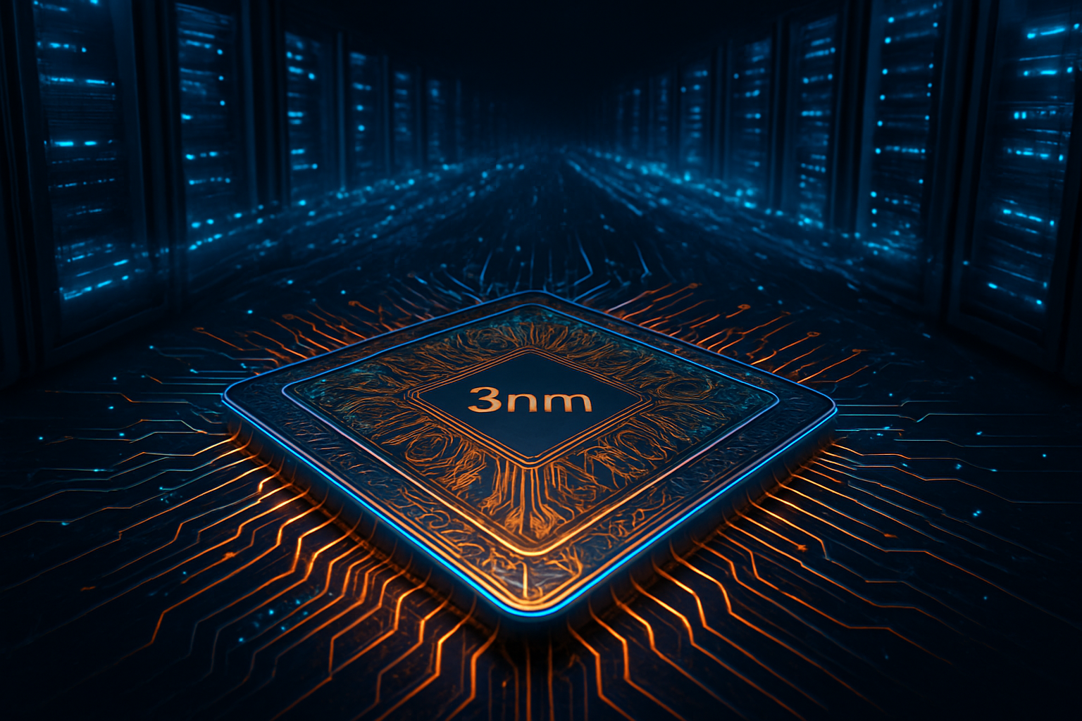
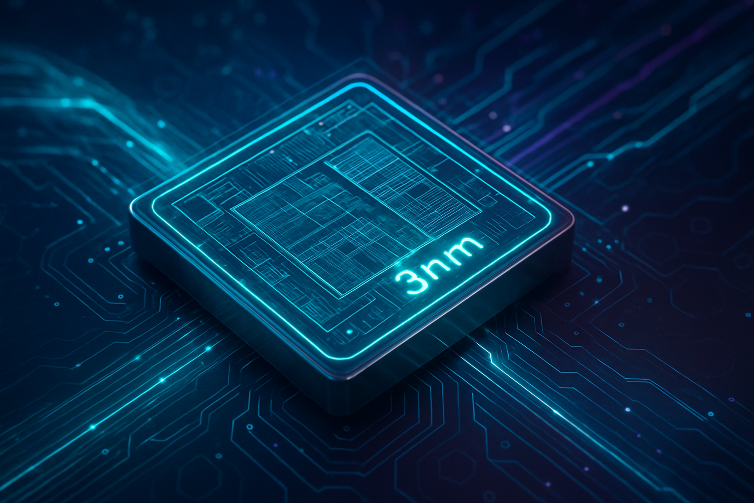
    Potential Concerns: Despite the immense potential, challenges persist. Cost remains a significant hurdle, with high upfront development costs for ASICs and neuromorphic chips (over $100 million for some designs). The complexity of designing and integrating these advanced chips, especially at smaller process nodes like 2nm, is escalating. Specialization lock-in is another concern; while efficient for specific tasks, a highly specialized chip may be inefficient or unsuitable for evolving AI models, potentially requiring costly redesigns. Furthermore, talent shortages in specialized fields like neuromorphic computing and the need for a robust software ecosystem for new architectures are critical challenges.

    Comparison to Previous Milestones: This trend represents an evolution from previous AI hardware milestones. The late 2000s saw the shift from CPUs to GPUs, which, with their parallel processing capabilities and platforms like NVIDIA's CUDA, offered dramatic speedups for AI. The current movement signifies a further refinement: moving beyond general-purpose GPUs to even more tailored solutions for optimal performance and efficiency, especially as generative AI pushes the limits of even advanced GPUs. This is analogous to how AI's specialized demands moved beyond general-purpose CPUs, now it's moving beyond general-purpose GPUs to even more granular, application-specific solutions.

    The Horizon: Charting Future AI Hardware Developments

    The trajectory of specialized AI chips points towards an exciting and rapidly evolving future, characterized by hybrid architectures, novel materials, and a relentless pursuit of efficiency.

    Near-Term Developments (Late 2024 and 2025): The market for AI ASICs is experiencing explosive growth, projected to reach $15 billion in 2025. Hyperscalers will continue to roll out custom silicon, and advancements in manufacturing processes like TSMC's (NYSE: TSM) 2nm process (expected in 2025) and Intel's 18A process node (late 2024/early 2025) will deliver significant power reductions. Neuromorphic computing will proliferate in edge AI and IoT devices, with chips like Intel's Loihi already being used in automotive applications. In-memory computing will see its first commercial deployments in data centers, driven by the demand for faster, more energy-efficient AI. Photonic AI chips will continue to demonstrate breakthroughs in energy efficiency and speed, with researchers showcasing chips 1,000 times more energy-efficient than NVIDIA's H100.

    Long-Term Developments (Beyond 2025): Experts predict the emergence of increasingly hybrid architectures, combining conventional CPU/GPU cores with specialized processors like neuromorphic chips. The industry will push beyond current technological boundaries, exploring novel materials, 3D architectures, and advanced packaging techniques like 3D stacking and chiplets. Photonic-electronic integration and the convergence of neuromorphic and photonic computing could lead to extremely energy-efficient AI. We may also see reconfigurable hardware or "software-defined silicon" that can adapt to diverse and rapidly evolving AI workloads.

    Potential Applications and Use Cases: Specialized AI chips are poised to revolutionize data centers (powering generative AI, LLMs, HPC), edge AI (smartphones, autonomous vehicles, robotics, smart cities), healthcare (diagnostics, drug discovery), finance, scientific research, and industrial automation. AI-enabled PCs are expected to make up 43% of all shipments by the end of 2025, and over 400 million GenAI smartphones are expected in 2025.

    Challenges and Expert Predictions: Manufacturing costs and complexity, power consumption and heat dissipation, the persistent "memory wall," and the need for robust software ecosystems remain significant challenges. Experts predict the global AI chip market could surpass $150 billion in 2025 and potentially reach $1.3 trillion by 2030. There will be a growing focus on optimizing for AI inference, intensified competition (with custom silicon challenging NVIDIA's dominance), and AI becoming the "backbone of innovation" within the semiconductor industry itself. The demand for High Bandwidth Memory (HBM) is so high that some manufacturers have nearly sold out their HBM capacity for 2025 and much of 2026, leading to "extreme shortages." Leading figures like OpenAI's Sam Altman and Google's Sundar Pichai warn that current hardware is a significant bottleneck for achieving Artificial General Intelligence (AGI), underscoring the need for radical innovation.

    The AI Hardware Renaissance: A Concluding Assessment

    The ongoing innovations in specialized semiconductor chips represent a pivotal moment in AI history, marking a decisive move towards hardware tailored precisely for the nuanced and demanding requirements of modern artificial intelligence. The key takeaway is clear: the era of "one size fits all" AI hardware is rapidly giving way to a diverse ecosystem of purpose-built processors.

    This development's significance cannot be overstated. By addressing the limitations of general-purpose hardware in terms of efficiency, speed, and power consumption, these specialized chips are not just enabling incremental improvements but are fundamental to unlocking the next generation of AI capabilities. They are making advanced AI more accessible, sustainable, and powerful, driving innovation across every sector. The long-term impact will be a world where AI is seamlessly integrated into nearly every device and system, operating with unprecedented efficiency and intelligence.

    In the coming weeks and months (late 2024 and 2025), watch for continued exponential market growth and intensified investment in specialized AI hardware. Keep an eye on startup innovation, particularly in analog, photonic, and memory-centric approaches, which will continue to challenge established players. Major tech companies will unveil and deploy new generations of their custom silicon, further solidifying the trend towards hybrid computing and the proliferation of Neural Processing Units (NPUs) in edge devices. Energy efficiency will remain a paramount design imperative, driving advancements in memory and interconnect architectures. Finally, breakthroughs in photonic chip maturation and broader adoption of neuromorphic computing at the edge will be critical indicators of the unfolding AI hardware renaissance.


    This content is intended for informational purposes only and represents analysis of current AI developments.

    TokenRing AI delivers enterprise-grade solutions for multi-agent AI workflow orchestration, AI-powered development tools, and seamless remote collaboration platforms.
    For more information, visit https://www.tokenring.ai/.

  • Chain Reaction Unleashes EL3CTRUM E31: A New Era of Efficiency in Bitcoin Mining Driven by Specialized Semiconductors

    Chain Reaction Unleashes EL3CTRUM E31: A New Era of Efficiency in Bitcoin Mining Driven by Specialized Semiconductors

    The cryptocurrency mining industry is buzzing with the recent announcement from Chain Reaction regarding its EL3CTRUM E31, a new suite of Bitcoin miners poised to redefine the benchmarks for energy efficiency and operational flexibility. This launch, centered around the groundbreaking EL3CTRUM A31 ASIC (Application-Specific Integrated Circuit), signifies a pivotal moment for large-scale mining operations, promising to significantly reduce operational costs and enhance profitability in an increasingly competitive landscape. With its cutting-edge 3nm process node technology, the EL3CTRUM E31 is not just an incremental upgrade but a generational leap, setting new standards for power efficiency and adaptability in the relentless pursuit of Bitcoin.

    The immediate significance of the EL3CTRUM E31 lies in its bold claim of delivering "sub-10 Joules per Terahash (J/TH)" efficiency, a metric that directly translates to lower electricity consumption per unit of computational power. This level of efficiency is critical as the global energy market remains volatile and environmental scrutiny on Bitcoin mining intensifies. Beyond raw power, the EL3CTRUM E31 emphasizes modularity, allowing miners to customize their infrastructure from the chip level up, and integrates advanced features like power curtailment and remote management. These innovations are designed to provide miners with unprecedented control and responsiveness to dynamic power markets, making the EL3CTRUM E31 a frontrunner in the race for sustainable and profitable Bitcoin production.

    Unpacking the Technical Marvel: The EL3CTRUM E31's Core Innovations

    At the heart of Chain Reaction's EL3CTRUM E31 system is the EL3CTRUM A31 ASIC, fabricated using an advanced 3nm process node. This miniaturization of transistor size is the primary driver behind its superior performance and energy efficiency. While samples are anticipated in May 2026 and volume shipments in Q3 2026, the projected specifications are already turning heads.

    The EL3CTRUM E31 is offered in various configurations to suit diverse operational needs and cooling infrastructures:

    • EL3CTRUM E31 Air: Offers a hash rate of 310 TH/s with 3472 W power consumption, achieving an efficiency of 11.2 J/TH.
    • EL3CTRUM E31 Hydro: Designed for liquid cooling, it boasts an impressive 880 TH/s hash rate at 8712 W, delivering a remarkable 9.9 J/TH efficiency.
    • EL3CTRUM E31 Immersion: Provides 396 TH/s at 4356 W, with an efficiency of 11.0 J/TH.

    The specialized ASICs are custom-designed for the SHA-256 algorithm used by Bitcoin, allowing them to perform this specific task with vastly greater efficiency than general-purpose CPUs or GPUs. Chain Reaction's commitment to pushing these boundaries is further evidenced by their active development of 2nm ASICs, promising even greater efficiencies in future iterations. This modular architecture, offering standalone A31 ASIC chips, H31 hashboards, and complete E31 units, empowers miners to optimize their systems for maximum scalability and a lower total cost of ownership. This flexibility stands in stark contrast to previous generations of more rigid, integrated mining units, allowing for tailored solutions based on regional power strategies, climate conditions, and existing facility infrastructure.

    Industry Ripples: Impact on Companies and Competitive Landscape

    The introduction of the EL3CTRUM E31 is set to create significant ripples across the Bitcoin mining industry, benefiting some while presenting formidable challenges to others. Chain Reaction, as the innovator behind this advanced technology, is positioned for substantial growth, leveraging its cutting-edge 3nm ASIC design and a robust supply chain.

    Several key players stand to benefit directly from this development. Core Scientific (NASDAQ: CORZ), a leading North American digital asset infrastructure provider, has a longstanding collaboration with Chain Reaction, recognizing ASIC innovation as crucial for differentiated infrastructure. This partnership allows Core Scientific to integrate EL3CTRUM technology to achieve superior efficiency and scalability. Similarly, ePIC Blockchain Technologies and BIT Mining Limited have also announced collaborations, aiming to deploy next-generation Bitcoin mining systems with industry-leading performance and low power consumption. For large-scale data center operators and industrial miners, the EL3CTRUM E31's efficiency and modularity offer a direct path to reduced operational costs and sustained profitability, especially in dynamic energy markets.

    Conversely, other ASIC manufacturers, such as industry stalwarts Bitmain and Whatsminer, will face intensified competitive pressure. The EL3CTRUM E31's "sub-10 J/TH" efficiency sets a new benchmark, compelling competitors to accelerate their research and development into smaller process nodes and more efficient architectures. Manufacturers relying on older process nodes or less efficient designs risk seeing their market share diminish if they cannot match Chain Reaction's performance metrics. This launch will likely hasten the obsolescence of current and older-generation mining hardware, forcing miners to upgrade more frequently to remain competitive. The emphasis on modular and customizable solutions could also drive a shift in the market, with large operators increasingly opting for components to integrate into custom data center designs, rather than just purchasing complete, off-the-shelf units.

    Wider Significance: Beyond the Mining Farm

    The advancements embodied by the EL3CTRUM E31 extend far beyond the immediate confines of Bitcoin mining, signaling broader trends within the technology and semiconductor industries. The relentless pursuit of efficiency and computational power in specialized hardware design mirrors the trajectory of AI, where purpose-built chips are essential for processing massive datasets and complex algorithms. While Bitcoin ASICs are distinct from AI chips, both fields benefit from the cutting-edge semiconductor manufacturing processes (e.g., 3nm, 2nm) that are pushing the limits of performance per watt.

    Intriguingly, there's a growing convergence between these sectors. Bitcoin mining companies, having established significant energy infrastructure, are increasingly exploring and even pivoting towards hosting AI and High-Performance Computing (HPC) operations. This synergy is driven by the shared need for substantial power and robust data center facilities. The expertise in managing large-scale digital infrastructure, initially developed for Bitcoin mining, is proving invaluable for the energy-intensive demands of AI, suggesting that advancements in Bitcoin mining hardware can indirectly contribute to the overall expansion of the AI sector.

    However, these advancements also bring wider concerns. While the EL3CTRUM E31's efficiency reduces energy consumption per unit of hash power, the overall energy consumption of the Bitcoin network remains a significant environmental consideration. As mining becomes more profitable, miners are incentivized to deploy more powerful hardware, increasing the total hash rate and, consequently, the network's total energy demand. The rapid technological obsolescence of mining hardware also contributes to a growing e-waste problem. Furthermore, the increasing specialization and cost of ASICs contribute to the centralization of Bitcoin mining, making it harder for individual miners to compete with large farms and potentially raising concerns about the network's decentralized ethos. The semiconductor industry, meanwhile, benefits from the demand but also faces challenges from the volatile crypto market and geopolitical tensions affecting supply chains. This evolution can be compared to historical tech milestones like the shift from general-purpose CPUs to specialized GPUs for graphics, highlighting a continuous trend towards optimized hardware for specific, demanding computational tasks.

    The Road Ahead: Future Developments and Expert Predictions

    The future of Bitcoin mining technology, particularly concerning specialized semiconductors, promises continued rapid evolution. In the near term (1-3 years), the industry will see a sustained push towards even smaller and more efficient ASIC chips. While 3nm ASICs like the EL3CTRUM A31 are just entering the market, the development of 2nm chips is already underway, with TSMC planning manufacturing by 2025 and Chain Reaction targeting a 2nm ASIC release in 2027. These advancements, leveraging innovative technologies like Gate-All-Around Field-Effect Transistors (GAAFETs), are expected to deliver further reductions in energy consumption and increases in processing speed. The entry of major players like Intel into the custom cryptocurrency product group also signals increased competition, which is likely to drive further innovation and potentially stabilize hardware pricing. Enhanced cooling solutions, such as hydro and immersion cooling, will also become increasingly standard to manage the heat generated by these powerful chips.

    Longer term (beyond 3 years), while the pursuit of miniaturization will continue, the fundamental economics of Bitcoin mining will undergo a significant shift. With the final Bitcoin projected to be mined around 2140, miners will eventually rely solely on transaction fees for revenue. This necessitates a robust fee market to incentivize miners and maintain network security. Furthermore, AI integration into mining operations is expected to deepen, optimizing power usage, hash rate performance, and overall operational efficiency. Beyond Bitcoin, the underlying technology of advanced ASICs holds potential for broader applications in High-Performance Computing (HPC) and encrypted AI computing, fields where Chain Reaction is already making strides with its "privacy-enhancing processors (3PU)."

    However, significant challenges remain. The ever-increasing network hash rate and difficulty, coupled with Bitcoin halving events (which reduce block rewards), will continue to exert immense pressure on miners to constantly upgrade equipment. High energy costs, environmental concerns, and semiconductor supply chain vulnerabilities exacerbated by geopolitical tensions will also demand innovative solutions and diversified strategies. Experts predict an unrelenting focus on efficiency, a continued geographic redistribution of mining power towards regions with abundant renewable energy and supportive policies, and intensified competition driving further innovation. Bullish forecasts for Bitcoin's price in the coming years suggest continued institutional adoption and market growth, which will sustain the incentive for these technological advancements.

    A Comprehensive Wrap-Up: Redefining the Mining Paradigm

    Chain Reaction's launch of the EL3CTRUM E31 marks a significant milestone in the evolution of Bitcoin mining technology. By leveraging advanced 3nm specialized semiconductors, the company is not merely offering a new product but redefining the paradigm for efficiency, modularity, and operational flexibility in the industry. The "sub-10 J/TH" efficiency target, coupled with customizable configurations and intelligent management features, promises substantial cost reductions and enhanced profitability for large-scale miners.

    This development underscores the critical role of specialized hardware in the cryptocurrency ecosystem and highlights the relentless pace of innovation driven by the demands of Proof-of-Work networks. It sets a new competitive bar for other ASIC manufacturers and will accelerate the obsolescence of less efficient hardware, pushing the entire industry towards more sustainable and technologically advanced solutions. While concerns around energy consumption, centralization, and e-waste persist, the EL3CTRUM E31 also demonstrates how advancements in mining hardware can intersect with and potentially benefit other high-demand computing fields like AI and HPC.

    Looking ahead, the industry will witness a continued "Moore's Law" effect in mining, with 2nm and even smaller chips on the horizon, alongside a growing emphasis on renewable energy integration and AI-driven operational optimization. The strategic partnerships forged by Chain Reaction with industry leaders like Core Scientific signal a collaborative approach to innovation that will be vital in navigating the challenges of increasing network difficulty and fluctuating market conditions. The EL3CTRUM E31 is more than just a miner; it's a testament to the ongoing technological arms race that defines the digital frontier, and its long-term impact will be keenly watched by tech journalists, industry analysts, and cryptocurrency enthusiasts alike in the weeks and months to come.

    This content is intended for informational purposes only and represents analysis of current AI developments.

    TokenRing AI delivers enterprise-grade solutions for multi-agent AI workflow orchestration, AI-powered development tools, and seamless remote collaboration platforms.
    For more information, visit https://www.tokenring.ai/.

  • The AI Supercycle: How ChatGPT Ignited a Gold Rush for Next-Gen Semiconductors

    The AI Supercycle: How ChatGPT Ignited a Gold Rush for Next-Gen Semiconductors

    The advent of ChatGPT and the subsequent explosion in generative artificial intelligence (AI) have fundamentally reshaped the technological landscape, triggering an unprecedented surge in demand for specialized semiconductors. This "post-ChatGPT boom" has not only accelerated the pace of AI innovation but has also initiated a profound transformation within the chip manufacturing industry, creating an "AI supercycle" that prioritizes high-performance computing and efficient data processing. The immediate significance of this trend is multifaceted, impacting everything from global supply chains and economic growth to geopolitical strategies and the very future of AI development.

    This dramatic shift underscores the critical role hardware plays in unlocking AI's full potential. As AI models grow exponentially in complexity and scale, the need for powerful, energy-efficient chips capable of handling immense computational loads has become paramount. This escalating demand is driving intense innovation in semiconductor design and manufacturing, creating both immense opportunities and significant challenges for chipmakers, AI companies, and national economies vying for technological supremacy.

    The Silicon Brains Behind the AI Revolution: A Technical Deep Dive

    The current AI boom is not merely increasing demand for chips; it's catalyzing a targeted demand for specific, highly advanced semiconductor types optimized for machine learning workloads. At the forefront are Graphics Processing Units (GPUs), which have emerged as the indispensable workhorses of AI. Companies like NVIDIA (NASDAQ: NVDA) have seen their market valuation and gross margins skyrocket due to their dominant position in this sector. GPUs, with their massively parallel architecture, are uniquely suited for the simultaneous processing of thousands of data points, a capability essential for the matrix operations and vector calculations that underpin deep learning model training and complex algorithm execution. This architectural advantage allows GPUs to accelerate tasks that would be prohibitively slow on traditional Central Processing Units (CPUs).

    Accompanying the GPU is High-Bandwidth Memory (HBM), a critical component designed to overcome the "memory wall" – the bottleneck created by traditional memory's inability to keep pace with GPU processing power. HBM provides significantly higher data transfer rates and lower latency by integrating memory stacks directly onto the same package as the processor. This close proximity enables faster communication, reduced power consumption, and massive throughput, which is crucial for AI model training, natural language processing, and real-time inference, where rapid data access is paramount.

    Beyond general-purpose GPUs, the industry is seeing a growing emphasis on Application-Specific Integrated Circuits (ASICs) and Neural Processing Units (NPUs). ASICs, exemplified by Google's (NASDAQ: GOOGL) Tensor Processing Units (TPUs), are custom-designed chips meticulously optimized for particular AI processing tasks, offering superior efficiency for specific workloads, especially for inference. NPUs, on the other hand, are specialized processors accelerating AI and machine learning tasks at the edge, in devices like smartphones and autonomous vehicles, where low power consumption and high performance are critical. This diversification reflects a maturing AI ecosystem, moving from generalized compute to specialized, highly efficient hardware tailored for distinct AI applications.

    The technical advancements in these chips represent a significant departure from previous computing paradigms. While traditional computing prioritized sequential processing, AI demands parallelization on an unprecedented scale. Modern AI chips feature smaller process nodes, advanced packaging techniques like 3D integrated circuit design, and innovative architectures that prioritize massive data throughput and energy efficiency. Initial reactions from the AI research community and industry experts have been overwhelmingly positive, with many acknowledging that these hardware breakthroughs are not just enabling current AI capabilities but are also paving the way for future, even more sophisticated, AI models and applications. The race is on to build ever more powerful and efficient silicon brains for the burgeoning AI mind.

    Reshaping the AI Landscape: Corporate Beneficiaries and Competitive Shifts

    The AI supercycle has profound implications for AI companies, tech giants, and startups, creating clear winners and intensifying competitive dynamics. Unsurprisingly, NVIDIA (NASDAQ: NVDA) stands as the primary beneficiary, having established a near-monopoly in high-end AI GPUs. Its CUDA platform and extensive software ecosystem further entrench its position, making it the go-to provider for training large language models and other complex AI systems. Other chip manufacturers like Advanced Micro Devices (NASDAQ: AMD) are aggressively pursuing the AI market, offering competitive GPU solutions and attempting to capture a larger share of this lucrative segment. Intel (NASDAQ: INTC), traditionally a CPU powerhouse, is also investing heavily in AI accelerators and custom silicon, aiming to reclaim relevance in this new computing era.

    Beyond the chipmakers, hyperscale cloud providers such as Microsoft (NASDAQ: MSFT), Amazon (NASDAQ: AMZN) (via AWS), and Google (NASDAQ: GOOGL) are heavily investing in AI-optimized infrastructure, often designing their own custom AI chips (like Google's TPUs) to gain a competitive edge in offering AI services and to reduce reliance on external suppliers. These tech giants are strategically positioning themselves as the foundational infrastructure providers for the AI economy, offering access to scarce GPU clusters and specialized AI hardware through their cloud platforms. This allows smaller AI startups and research labs to access the necessary computational power without the prohibitive upfront investment in hardware.

    The competitive landscape for major AI labs and startups is increasingly defined by access to these powerful semiconductors. Companies with strong partnerships with chip manufacturers or those with the resources to secure massive GPU clusters gain a significant advantage in model development and deployment. This can potentially disrupt existing product or services markets by enabling new AI-powered capabilities that were previously unfeasible. However, it also creates a divide, where smaller players might struggle to compete due to the high cost and scarcity of these essential resources, leading to concerns about "access inequality." The strategic advantage lies not just in innovative algorithms but also in the ability to secure and deploy the underlying silicon.

    The Broader Canvas: AI's Impact on Society and Technology

    The escalating demand for AI-specific semiconductors is more than just a market trend; it's a pivotal moment in the broader AI landscape, signaling a new era of computational intensity and technological competition. This fits into the overarching trend of AI moving from theoretical research to widespread application across virtually every industry, from healthcare and finance to autonomous vehicles and natural language processing. The sheer scale of computational resources now required for state-of-the-art AI models, particularly generative AI, marks a significant departure from previous AI milestones, where breakthroughs were often driven more by algorithmic innovations than by raw processing power.

    However, this accelerated demand also brings potential concerns. The most immediate is the exacerbation of semiconductor shortages and supply chain challenges. The global semiconductor industry, still recovering from previous disruptions, is now grappling with an unprecedented surge in demand for highly specialized components, with over half of industry leaders doubting their ability to meet future needs. This scarcity drives up prices for GPUs and HBM, creating significant cost barriers for AI development and deployment. Furthermore, the immense energy consumption of AI servers, packed with these powerful chips, raises environmental concerns and puts increasing strain on global power grids, necessitating urgent innovations in energy efficiency and data center architecture.

    Comparisons to previous technological milestones, such as the internet boom or the mobile revolution, are apt. Just as those eras reshaped industries and societies, the AI supercycle, fueled by advanced silicon, is poised to do the same. However, the geopolitical implications are arguably more pronounced. Semiconductors have transcended their role as mere components to become strategic national assets, akin to oil. Access to cutting-edge chips directly correlates with a nation's AI capabilities, making it a critical determinant of military, economic, and technological power. This has fueled "techno-nationalism," leading to export controls, supply chain restrictions, and massive investments in domestic semiconductor production, particularly evident in the ongoing technological rivalry between the United States and China, aiming for technological sovereignty.

    The Road Ahead: Future Developments and Uncharted Territories

    Looking ahead, the future of AI and semiconductor technology promises continued rapid evolution. In the near term, we can expect relentless innovation in chip architectures, with a focus on even smaller process nodes (e.g., 2nm and beyond), advanced 3D stacking techniques, and novel memory solutions that further reduce latency and increase bandwidth. The convergence of hardware and software co-design will become even more critical, with chipmakers working hand-in-hand with AI developers to optimize silicon for specific AI frameworks and models. We will also see a continued diversification of AI accelerators, moving beyond GPUs to more specialized ASICs and NPUs tailored for specific inference tasks at the edge and in data centers, driving greater efficiency and lower power consumption.

    Long-term developments include the exploration of entirely new computing paradigms, such as neuromorphic computing, which aims to mimic the structure and function of the human brain, offering potentially massive gains in energy efficiency and parallel processing for AI. Quantum computing, while still in its nascent stages, also holds the promise of revolutionizing AI by solving problems currently intractable for even the most powerful classical supercomputers. These advancements will unlock a new generation of AI applications, from hyper-personalized medicine and advanced materials discovery to fully autonomous systems and truly intelligent conversational agents.

    However, significant challenges remain. The escalating cost of chip design and fabrication, coupled with the increasing complexity of manufacturing, poses a barrier to entry for new players and concentrates power among a few dominant firms. The supply chain fragility, exacerbated by geopolitical tensions, necessitates greater resilience and diversification. Furthermore, the energy footprint of AI remains a critical concern, demanding continuous innovation in low-power chip design and sustainable data center operations. Experts predict a continued arms race in AI hardware, with nations and companies pouring resources into securing their technological future. The next few years will likely see intensified competition, strategic alliances, and breakthroughs that further blur the lines between hardware and intelligence.

    Concluding Thoughts: A Defining Moment in AI History

    The post-ChatGPT boom and the resulting surge in semiconductor demand represent a defining moment in the history of artificial intelligence. It underscores a fundamental truth: while algorithms and data are crucial, the physical infrastructure—the silicon—is the bedrock upon which advanced AI is built. The shift towards specialized, high-performance, and energy-efficient chips is not merely an incremental improvement; it's a foundational change that is accelerating the pace of AI development and pushing the boundaries of what machines can achieve.

    The key takeaways from this supercycle are clear: GPUs and HBM are the current kings of AI compute, driving unprecedented market growth for companies like NVIDIA; the competitive landscape is being reshaped by access to these scarce resources; and the broader implications touch upon national security, economic power, and environmental sustainability. This development highlights the intricate interdependence between hardware innovation and AI progress, demonstrating that neither can advance significantly without the other.

    In the coming weeks and months, we should watch for several key indicators: continued investment in advanced semiconductor manufacturing facilities (fabs), particularly in regions aiming for technological sovereignty; the emergence of new AI chip architectures and specialized accelerators from both established players and innovative startups; and how geopolitical dynamics continue to influence the global semiconductor supply chain. The AI supercycle is far from over; it is an ongoing revolution that promises to redefine the technological and societal landscape for decades to come.

    This content is intended for informational purposes only and represents analysis of current AI developments.

    TokenRing AI delivers enterprise-grade solutions for multi-agent AI workflow orchestration, AI-powered development tools, and seamless remote collaboration platforms.
    For more information, visit https://www.tokenring.ai/.