The semiconductor industry has reached a pivotal milestone in the race toward sub-2nm chip production. As of February 2026, ZEISS SMT has officially commenced the global deployment of its AIMS® EUV 3.0 systems to all major semiconductor fabs. This next-generation actinic mask qualification system is the final piece of the infrastructure puzzle required for High-NA (High Numerical Aperture) EUV lithography, providing the essential "gatekeeping" technology that ensures photomasks are defect-free before they enter the world’s most advanced lithography scanners.
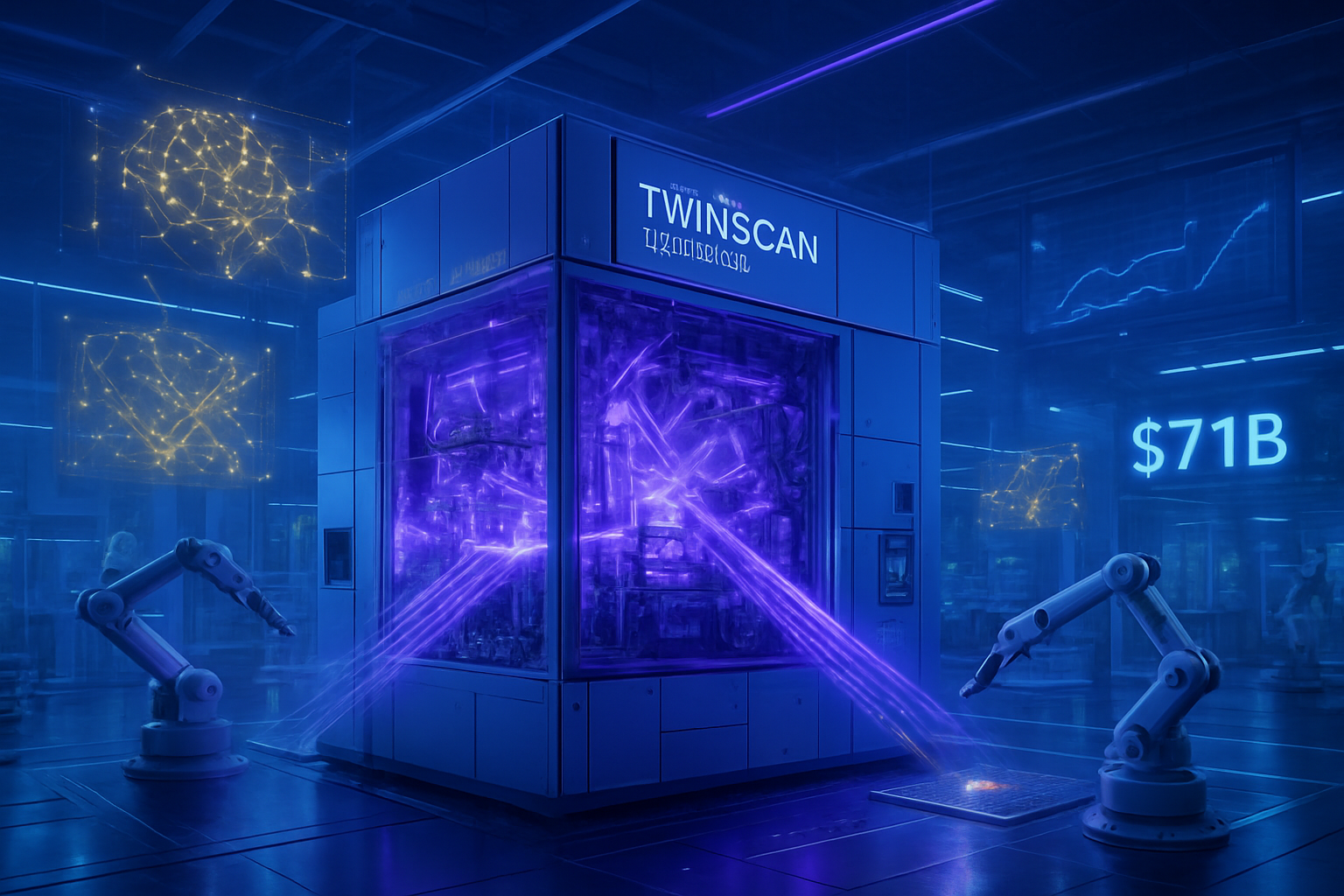
The significance of this deployment cannot be overstated. By enabling the production of 2nm and 1.4nm chips with three times the throughput of previous systems, the AIMS EUV 3.0 effectively removes a massive metrology bottleneck that threatened to stall the progress of AI hardware. As the industry transitions to the next generation of silicon, this platform ensures that the massive investments made in High-NA lithography by giants like ASML Holding N.V. (NASDAQ: ASML) and Intel Corporation (NASDAQ: INTC) translate into viable commercial yields for the AI era.
The Technical Backbone: "Seeing What the Scanner Sees"
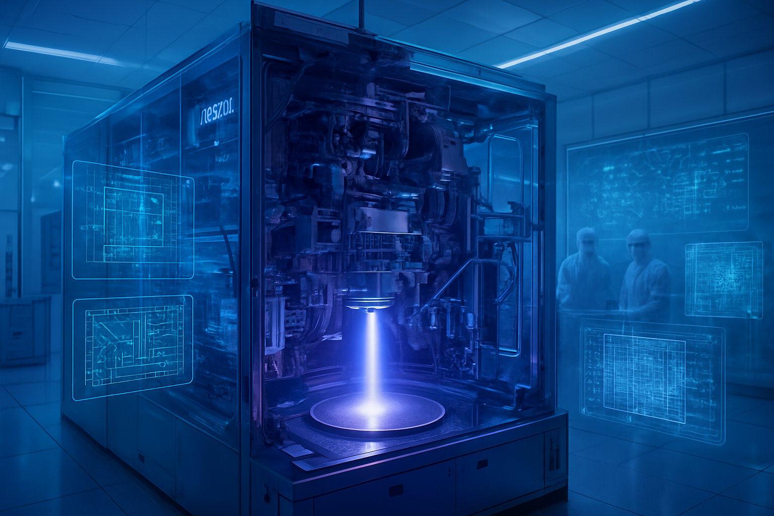
At the heart of the AIMS EUV 3.0 system is its "actinic" capability, meaning it utilizes the exact same 13.5nm wavelength of light as the EUV scanners themselves. Traditional mask inspection tools, which often use deep-ultraviolet (DUV) light or electron beams, can struggle to detect defects buried deep within the complex multi-layers of an EUV mask. The AIMS system solves this by emulating the optical conditions of the scanner perfectly, allowing engineers to verify that a mask will produce a perfect pattern on the wafer. This "aerial image" measurement is critical for identifying "invisible" defects that only manifest when hit by EUV radiation.
The 3.0 generation introduces a breakthrough known as "Digital FlexIllu," a digital emulation technology that replicates any complex illumination setting of an ASML scanner without the need for physical hardware changes. Previously, switching between different aperture settings was a time-consuming mechanical process. With Digital FlexIllu, the system can pivot instantly, allowing for rapid testing of various designs. This flexibility is a major driver behind the system's 3x throughput increase, enabling fabs to qualify more masks in a fraction of the time required by the previous AIMS EUV generation.
Perhaps most critically, the AIMS EUV 3.0 is the first platform to support both standard 0.33 NA and the new 0.55 High-NA anamorphic imaging. Because High-NA EUV uses lenses that magnify differently in the X and Y directions, the mask qualification process becomes exponentially more complex. The AIMS 3.0 emulates this anamorphic profile with precision, achieving phase metrology reproducibility rated well below 0.5 degrees. This level of accuracy is mandatory for the production of the ultra-dense transistor arrays found in upcoming sub-2nm designs.
Initial reactions from the semiconductor research community have been overwhelmingly positive. Dr. Clemens Neuenhahn, Head of ZEISS Semiconductor Mask Solutions, has emphasized that this system is the key to cost-effective and sustainable microchip production. Experts at industry forums like SPIE have noted that while the High-NA scanners themselves are the "engines" of the next node, the AIMS 3.0 is the "navigation system" that ensures those engines don't waste expensive time and silicon on faulty masks.
Strategic Impact on the Foundry Landscape
The deployment of AIMS EUV 3.0 creates a new competitive landscape for the world’s leading foundries. Intel Corporation (NASDAQ: INTC) has been the most aggressive adopter, positioning itself as the first company to integrate High-NA EUV into its "5 nodes in 4 years" strategy. By securing early access to the AIMS 3.0 platform, Intel aims to solidify its lead in the 1.4nm (Intel 14A) era, moving toward single-exposure patterning that could drastically reduce manufacturing complexity and cost compared to current multi-patterning techniques.
Samsung Electronics Co., Ltd. (KRX: 005930) has also made the AIMS EUV 3.0 a cornerstone of its "triangular alliance" with ASML and ZEISS. Samsung plans to deploy these systems at its Pyeongtaek and Taylor, Texas facilities to support its 2nm and 1.4nm roadmaps. For Samsung, the 3x throughput increase is vital for scaling its foundry business and closing the gap with market leaders, as it allows for faster iteration on the high-performance computing (HPC) and AI chips that are currently in high demand.
Taiwan Semiconductor Manufacturing Company (TSMC) (NYSE: TSM), while typically more conservative in its public High-NA timeline, is confirmed to be among the primary users of the AIMS 3.0 platform. TSMC’s R&D centers in Taiwan are utilizing the tool to refine its A16 and N2 processes. The system’s ability to handle the "Wafer-Level Critical Dimension" (WLCD) option—a new 2026 feature that predicts how mask defects will specifically impact final chip dimensions—gives TSMC a powerful tool to maintain its legendary yield rates even as features shrink to the atomic scale.
The broader business implication is a shift in the "metrology-to-lithography" ratio. As scanners become more expensive—with High-NA units costing upwards of $350 million—the cost of downtime due to a bad mask becomes catastrophic. The AIMS EUV 3.0 serves as an essential "insurance policy" for these foundries, ensuring that every hour of scanner time is spent on defect-free production. This helps stabilize the massive capital expenditures required for 2nm fabrication.
Powering the Next Generation of AI Hardware
The arrival of the AIMS EUV 3.0 is inextricably linked to the roadmap of AI chip designers like NVIDIA Corporation (NASDAQ: NVDA) and Advanced Micro Devices, Inc. (NASDAQ: AMD). These companies are moving toward a one-year product cadence, with NVIDIA’s "Vera Rubin" and AMD’s "Instinct MI400" series expected to push the boundaries of transistor density. Without the throughput and accuracy provided by the AIMS 3.0, the masks required for these massive AI dies could not be produced at the volume or reliability needed to meet global demand.
This development fits into a broader trend of "AI-ready" infrastructure. As Large Language Models (LLMs) and generative AI continue to demand more compute power, the industry is hitting the physical limits of current 3nm processes. The transition to 2nm and 1.4nm, enabled by High-NA and AIMS 3.0, is expected to provide the 15-30% performance-per-watt gains necessary to keep AI scaling viable. By ensuring that High-NA masks are production-ready, ZEISS has effectively cleared the "logistics bottleneck" for the next three years of AI hardware evolution.
However, the shift also raises concerns about the concentration of technology. With only one company in the world (ZEISS) capable of producing these actinic mask review systems, the semiconductor supply chain remains highly centralized. Any disruption in ZEISS’s production could ripple through the entire industry, potentially delaying the rollout of future AI GPUs. This has led to increased calls for "supply chain resilience" and closer collaboration between governments and the "lithography trio" of ASML, ZEISS, and the leading foundries.
Compared to previous milestones, such as the initial introduction of EUV in 2019, the AIMS 3.0 deployment feels more mature and integrated. While early EUV adoption was plagued by low yields and metrology gaps, the High-NA era is launching with a much more robust support ecosystem. This suggests that the ramp-up for 2nm and 1.4nm chips may be smoother than the industry's difficult transition to 5nm and 7nm.
The Road to 1nm and Beyond
Looking ahead, the AIMS EUV 3.0 is designed to be a long-term platform. Experts predict that it will remain the workhorse of mask qualification through the end of the decade, supporting the transition from the 1.4nm node to the "Angstrom era" of 1nm (A10) and beyond. The modular nature of the system allows for future upgrades to software-based metrology, such as AI-driven defect classification, which could further increase throughput without requiring new hardware.
In the near term, we can expect to see the first "AIMS-qualified" High-NA chips hitting the market in late 2026 and early 2027. These will likely be the high-end data center GPUs and specialized AI accelerators that form the backbone of the next generation of supercomputers. The challenge now shifts to the mask shops themselves, which must scale their own internal processes to match the blistering pace enabled by the AIMS 3.0.
Industry analysts expect that by 2028, the "Digital FlexIllu" technology pioneered here will become a standard requirement for all metrology tools. As the industry moves toward "Hyper-NA" (even higher numerical apertures), the lessons learned from the AIMS 3.0 deployment will serve as the blueprint for the next twenty years of semiconductor scaling.
A New Chapter in Moore’s Law
The global deployment of ZEISS SMT’s AIMS EUV 3.0 marks a definitive "go-live" for the High-NA era. By solving the dual challenges of actinic accuracy and high throughput, ZEISS has provided the semiconductor industry with the tools it needs to continue the aggressive scaling required by the AI revolution. The system’s ability to emulate the most complex optical conditions of ASML’s $350 million scanners ensures that "the heart of lithography"—the photomask—is no longer a point of failure.
This development is a significant chapter in the history of Moore’s Law. It proves that despite the immense physical and optical challenges of sub-2nm manufacturing, the synergy between European optics, Dutch lithography, and global foundry expertise remains capable of breaking through technological plateaus. For AI companies, it is a signal that the hardware runway is clear for the next several generations of breakthroughs.
In the coming weeks and months, the industry will be watching for the first yield reports from Intel and Samsung as they integrate these systems into their HVM (High Volume Manufacturing) lines. These results will be the ultimate proof of whether the AIMS EUV 3.0 has successfully future-proofed the silicon foundations of the AI age.
This content is intended for informational purposes only and represents analysis of current AI developments.
TokenRing AI delivers enterprise-grade solutions for multi-agent AI workflow orchestration, AI-powered development tools, and seamless remote collaboration platforms.
For more information, visit https://www.tokenring.ai/.