Tag: ASML

  • The High-NA Era Arrives: How Intel’s $380M Lithography Bet is Redefining AI Silicon

    The High-NA Era Arrives: How Intel’s $380M Lithography Bet is Redefining AI Silicon

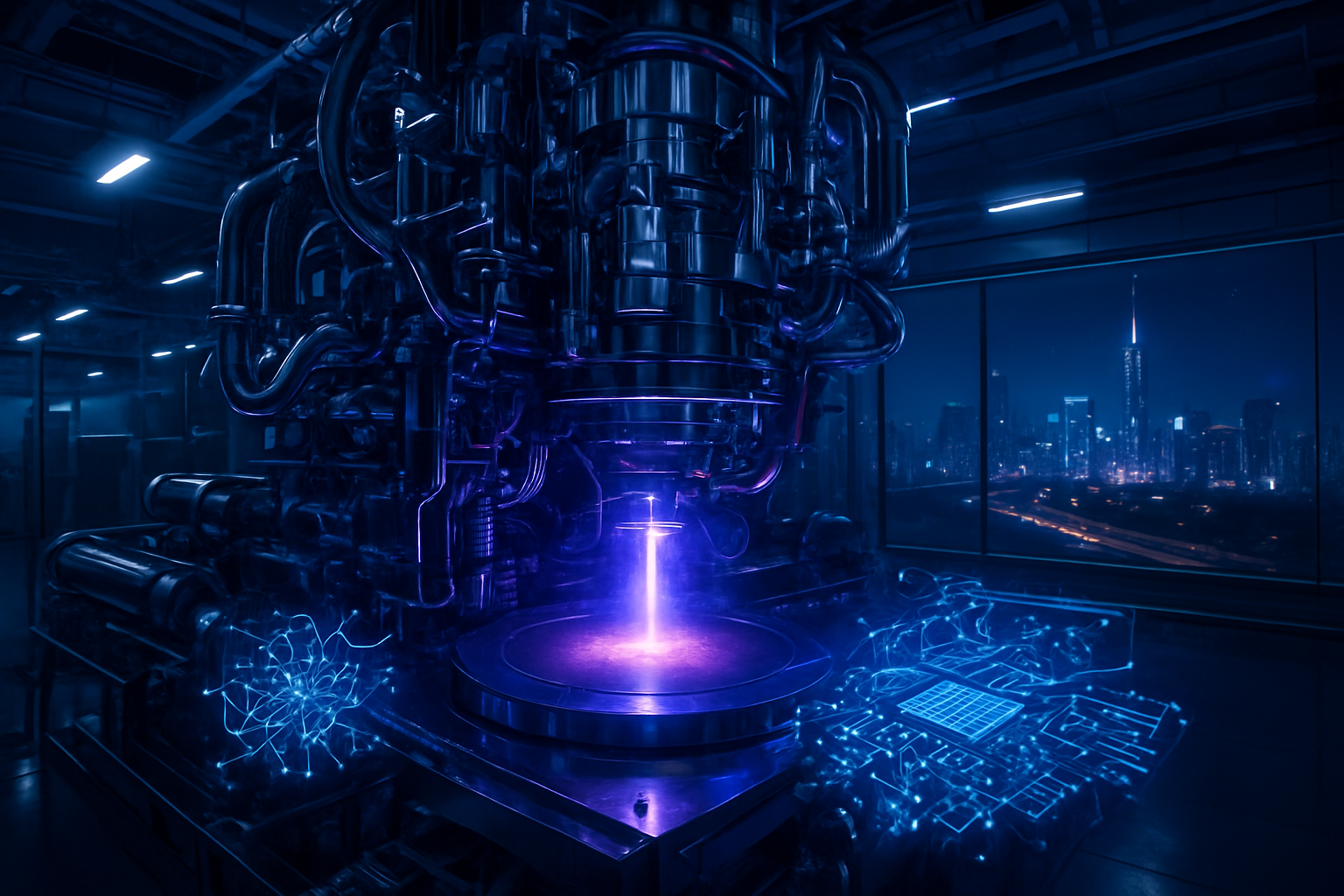
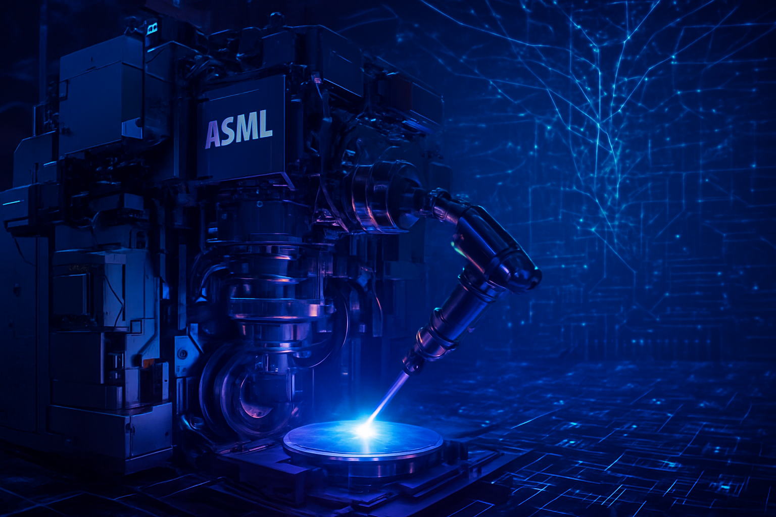
    The dawn of 2026 marks a historic inflection point in the semiconductor industry as the "mass production era" of High-Numerical Aperture (High-NA) Extreme Ultraviolet (EUV) lithography officially moves from laboratory speculation to the factory floor. Leading the charge, Intel (NASDAQ: INTC) has confirmed the completion of acceptance testing for its latest fleet of ASML (NASDAQ: ASML) Twinscan EXE:5200 systems, signaling the start of a multi-year transition toward the 1.4nm (14A) node. With each machine carrying a price tag exceeding $380 million, this development represents one of the most expensive and technically demanding gambles in industrial history, aimed squarely at sustaining the hardware requirements of the generative AI revolution.

    The significance of this transition cannot be overstated for the future of artificial intelligence. As transformer models grow in complexity, the demand for processors with higher transistor densities and lower power profiles has hit a physical wall with traditional EUV technology. By deploying High-NA tools, chipmakers are now able to print features with a resolution of approximately 8nm—nearly doubling the precision of previous generations. This shift is not merely an incremental upgrade; it is a fundamental reconfiguration of the economics of scaling, moving the industry toward a future where 1nm processors will eventually power the next decade of autonomous systems and trillion-parameter AI models.

    The Physics of 0.55 NA: A New Blueprint for Transistors

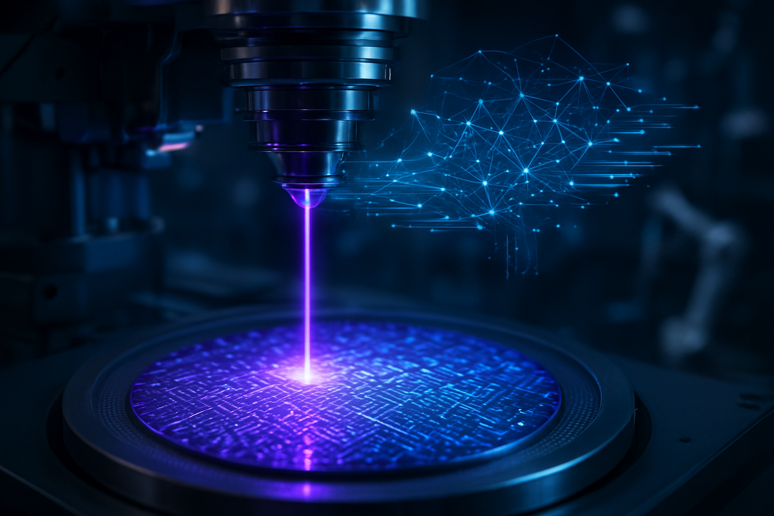
    At the heart of this revolution is ASML’s Twinscan EXE series, which increases the Numerical Aperture (NA) from 0.33 to 0.55. In practical terms, this allows the lithography machine to focus light more sharply, enabling the printing of significantly smaller features on a silicon wafer. While standard EUV tools required "multi-patterning"—a process of printing a single layer multiple times to achieve higher resolution—High-NA EUV enables single-exposure patterning for the most critical layers of a chip. This reduction in process complexity is expected to improve yields and shorten the time-to-market for cutting-edge AI accelerators, which have historically been plagued by the intricate manufacturing requirements of sub-3nm nodes.

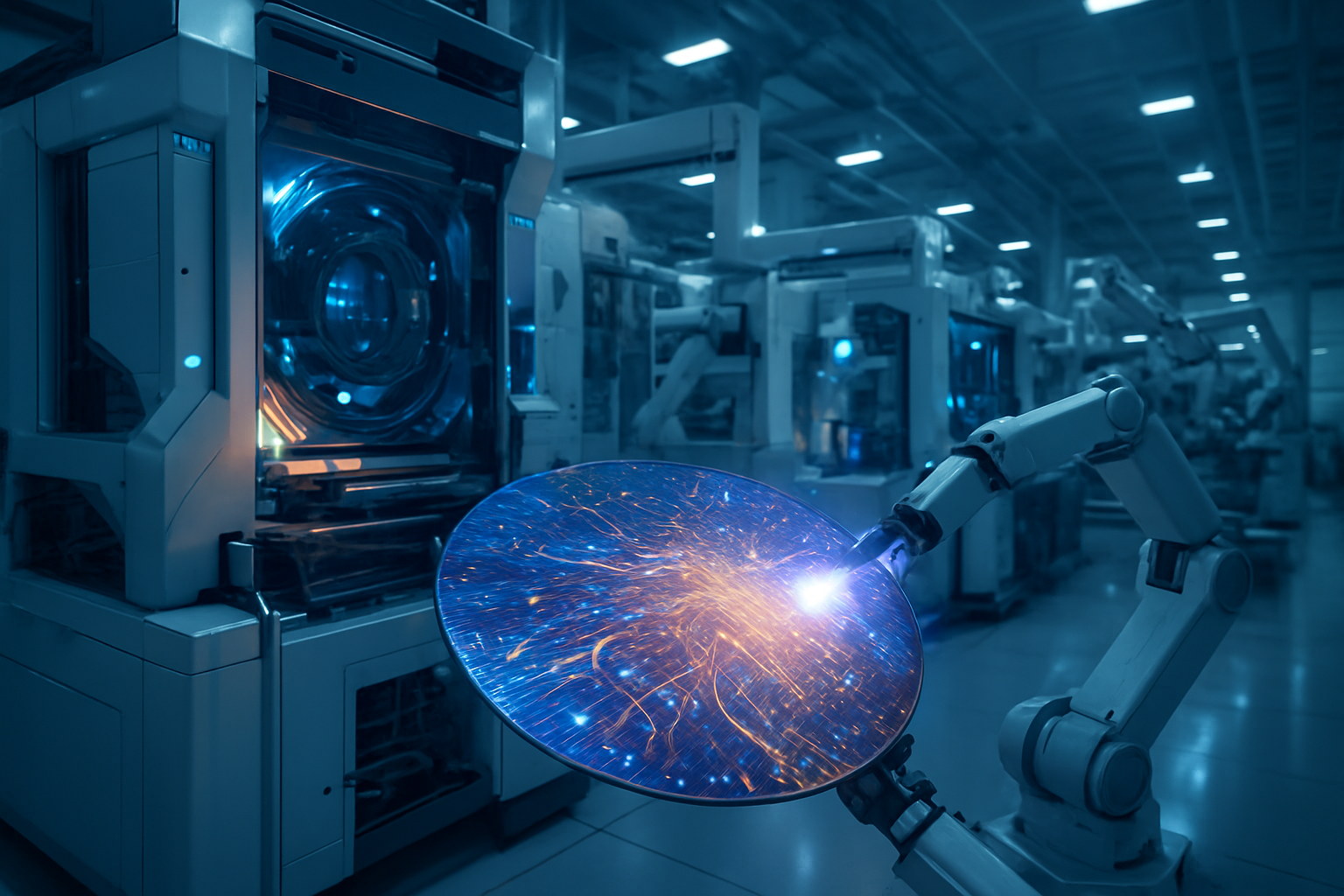
    Technically, the transition to High-NA introduces an "anamorphic" optical system, which magnifies the X and Y axes differently. This design results in a "half-field" exposure, meaning the reticle size is effectively halved compared to standard EUV. To manufacture the massive dies required for high-end AI GPUs, such as those produced by NVIDIA (NASDAQ: NVDA), manufacturers must now employ "stitching" techniques to join two exposure fields into a single seamless pattern. This architectural shift has sparked intense discussion among AI researchers and hardware engineers, as it necessitates a move toward "chiplet" designs where multiple smaller dies are interconnected, rather than relying on a single monolithic slab of silicon.

    Intel’s primary vehicle for this technology is the 14A node, the world’s first process built from the ground up to be "High-NA native." Initial reports from Intel’s D1X facility in Oregon suggest that the EXE:5200B tools are achieving throughputs of over 220 wafers per hour, a critical metric for high-volume manufacturing. Industry experts note that while the $380 million capital expenditure per tool is staggering, the ability to eliminate multiple mask steps in the production cycle could eventually offset these costs, provided the volume of AI-specific silicon remains high.

    A High-Stakes Rivalry: Intel vs. Samsung and the "Lithography Divide"

    The deployment of High-NA EUV has created a strategic divide among the world’s three leading foundries. Intel’s aggressive "first-mover" advantage is a calculated attempt to regain process leadership after losing ground to competitors over the last decade. By securing the earliest shipments of the EXE:5200 series, Intel is positioning itself as the premier destination for custom AI silicon from tech giants like Microsoft (NASDAQ: MSFT) and Amazon (NASDAQ: AMZN), who are increasingly looking to design their own proprietary chips to optimize AI workloads.

    Samsung (KRX: 005930), meanwhile, has taken a dual-track approach. Having received its first High-NA units in 2025, the South Korean giant is integrating the technology into both its logic foundry and its advanced memory production. For Samsung, High-NA is essential for the development of HBM4 (High Bandwidth Memory), the specialized memory that feeds data to AI processors. The precision of High-NA is vital for the extreme vertical stacking required in next-generation HBM, making Samsung a formidable competitor in the AI hardware supply chain.

    In contrast, Taiwan Semiconductor Manufacturing Company (NYSE: TSM) has maintained a more conservative stance, opting to refine its existing 0.33 NA EUV processes for its 2nm (N2) node. This has created a "lithography divide" where Intel and Samsung are betting on the raw resolution of High-NA, while TSMC relies on its proven manufacturing excellence and cost-efficiency. The competitive implication is clear: if High-NA enables Intel to hit the 1.4nm milestone ahead of schedule, the balance of power in the global semiconductor market could shift back toward American and Korean soil for the first time in years.

    Moore’s Law and the Energy Crisis of AI

    The broader significance of the High-NA era lies in its role as a "lifeline" for Moore’s Law. For years, critics have predicted the end of transistor scaling, arguing that the heat and physical limitations of sub-atomically small components would eventually halt progress. High-NA EUV, combined with new transistor architectures like Gate-All-Around (GAA) and backside power delivery, provides a roadmap for another decade of scaling. This is particularly vital as the AI landscape shifts from "training" large models to "inference" at the edge, where energy efficiency is the primary constraint.

    Processors manufactured on the 1.4nm and 1nm nodes are expected to deliver up to a 30% reduction in power consumption compared to current 3nm chips. In an era where AI data centers are consuming an ever-larger share of the global power grid, these efficiency gains are not just an economic advantage—they are a geopolitical and environmental necessity. Without the scaling enabled by High-NA, the projected growth of generative AI would likely be throttled by the sheer energy requirements of the hardware needed to support it.

    However, the transition is not without its concerns. The extreme cost of High-NA tools threatens to centralize chip manufacturing even further, as only a handful of companies can afford the multi-billion dollar investment required to build a High-NA-capable "mega-fab." This concentration of advanced manufacturing capabilities raises questions about supply chain resilience and the accessibility of cutting-edge hardware for smaller AI startups. Furthermore, the technical challenges of "stitching" half-field exposures could lead to initial yield issues, potentially keeping prices high for the very AI chips the technology is meant to proliferate.

    The Road to 1.4nm and Beyond

    Looking ahead, the next 24 to 36 months will be focused on perfecting the transition from pilot production to High-Volume Manufacturing (HVM). Intel is targeting 2027 for the full commercialization of its 14A node, with Samsung likely following closely behind with its SF1.4 process. Beyond that, the industry is already eyeing the 1nm milestone—often referred to as the "Angstrom era"—where features will be measured at the scale of individual atoms.

    Future developments will likely involve the integration of High-NA with even more exotic materials and architectures. We can expect to see the rise of "2D semiconductors" and "carbon nanotube" components that take advantage of the extreme resolution provided by ASML’s optics. Additionally, as the physical limits of light-based lithography are reached, researchers are already exploring "Hyper-NA" systems with even higher apertures, though such technology remains in the early R&D phase.

    The immediate challenge remains the optimization of the photoresist chemicals and mask technology used within the High-NA machines. At such small scales, "stochastic effects"—random variations in the way light interacts with matter—become a major source of defects. Solving these material science puzzles will be the primary focus of the engineering community throughout 2026, as they strive to make the 1.4nm roadmap a reality for the mass market.

    A Watershed Moment for AI Infrastructure

    The arrival of the High-NA EUV mass production era is a watershed moment for the technology industry. It represents the successful navigation of one of the most difficult engineering hurdles in human history, ensuring that the physical hardware of the AI age can continue to evolve alongside the software. For Intel, it is a "do-or-die" moment to reclaim its crown; for Samsung, it is an opportunity to dominate both the brain (logic) and the memory of future AI systems.

    In summary, the transition to 0.55 NA lithography marks the end of the "low-resolution" era of semiconductor manufacturing. While the $380 million price tag per machine is a barrier to entry, the potential for 2.9x increases in transistor density offers a clear path toward the 1.4nm and 1nm chips that will define the late 2020s. The industry has effectively doubled down on hardware scaling to meet the insatiable appetite of AI.

    In the coming months, watchers should keep a close eye on the first "test chips" emerging from Intel’s 14A pilot lines. The success or failure of these early runs will dictate the pace of AI hardware advancement for the rest of the decade. As the first High-NA-powered processors begin to power the next generation of data centers, the true impact of this $380 million gamble will finally be revealed in the speed and efficiency of the AI models we use every day.


    This content is intended for informational purposes only and represents analysis of current AI developments.

    TokenRing AI delivers enterprise-grade solutions for multi-agent AI workflow orchestration, AI-powered development tools, and seamless remote collaboration platforms.
    For more information, visit https://www.tokenring.ai/.

  • ASML Enters the “Angstrom Era”: How Intel and TSMC’s Record Capex is Fueling the High-NA EUV Revolution

    ASML Enters the “Angstrom Era”: How Intel and TSMC’s Record Capex is Fueling the High-NA EUV Revolution

    As the global technology industry crosses into 2026, ASML (NASDAQ:ASML) has officially cemented its role as the ultimate gatekeeper of the artificial intelligence revolution. Following a fiscal 2025 that saw unprecedented demand for AI-specific silicon, ASML’s 2026 outlook points to a historic revenue target of €36.5 billion. This growth is being propelled by a massive capital expenditure surge from industry titans Intel (NASDAQ:INTC) and TSMC (NYSE:TSM), who are locked in a high-stakes "Race to 2nm" and beyond. The centerpiece of this transformation is the transition of High-NA (Numerical Aperture) Extreme Ultraviolet (EUV) lithography from experimental pilot lines into high-volume manufacturing (HVM).

    The immediate significance of this development cannot be overstated. With Big Tech projected to invest over $400 billion in AI infrastructure in 2026 alone, the bottleneck has shifted from software algorithms to the physical limits of silicon. ASML’s delivery of the Twinscan EXE:5200 systems represents the first time the semiconductor industry can reliably print features at the angstrom scale in a commercial environment. This technological leap is the primary engine allowing chipmakers to keep pace with the exponential compute requirements of next-generation Large Language Models (LLMs) and autonomous AI agents.

    The Technical Edge: Twinscan EXE:5200 and the 8nm Resolution Frontier

    At the heart of the 2026 roadmap is the Twinscan EXE:5200, ASML’s flagship High-NA EUV system. Unlike the previous generation of standard (Low-NA) EUV tools that utilized a 0.33 numerical aperture, the High-NA systems utilize a 0.55 NA lens system. This allows for a resolution of 8nm, enabling the printing of features that are 1.7 times smaller than what was previously possible. For engineers, this means the ability to achieve a 2.9x increase in transistor density without the need for complex, yield-killing multi-patterning techniques.

    The EXE:5200 is a significant upgrade over the R&D-focused EXE:5000 models delivered in 2024 and 2025. It boasts a productivity throughput of over 200 wafers per hour (WPH), matching the efficiency of standard EUV tools while operating at a far tighter resolution. This throughput is critical for the commercial viability of 2nm and 1.4nm (14A) nodes. By moving to a single-exposure process for the most critical metal layers of a chip, manufacturers can reduce cycle times and minimize the cumulative defects that occur when a single layer must be passed through a scanner multiple times.

    Initial reactions from the industry have been polarized along strategic lines. Intel, which received the world’s first commercial-grade EXE:5200B in late 2025, has championed the tool as the "holy grail" of process leadership. Conversely, experts at TSMC initially expressed caution regarding the system's $400 million price tag, preferring to push standard EUV to its absolute limits. However, as of early 2026, the sheer complexity of 1.6nm (A16) and 1.4nm designs has forced a universal consensus: High-NA is no longer an optional luxury but a fundamental requirement for the "Angstrom Era."

    Strategic Warfare: Intel’s First-Mover Gamble vs. TSMC’s Efficiency Engine

    The competitive landscape of 2026 is defined by a sharp divergence in how the world’s two largest foundries are deploying ASML’s technology. Intel has adopted an aggressive "first-mover" strategy, utilizing High-NA EUV to accelerate its 14A (1.4nm) node. By integrating these tools earlier than its rivals, Intel aims to reclaim the process leadership it lost a decade ago. For Intel, 2026 is the "prove-it" year; if the EXE:5200 can deliver superior yields for its Panther Lake and Clearwater Forest processors, the company will have a strategic advantage in attracting external foundry customers like Microsoft (NASDAQ:MSFT) and Nvidia (NASDAQ:NVDA).

    TSMC, meanwhile, is operating with a massive 2026 capex budget of $52 billion to $56 billion, much of which is dedicated to the high-volume ramp of its N2 (2nm) and N2P nodes. While TSMC has been more conservative with High-NA adoption—relying on standard EUV with advanced multi-patterning for its A16 (1.6nm) process—the company has begun installing High-NA evaluation tools in early 2026 to de-risk its future A10 node. TSMC’s strategy focuses on maximizing the ROI of its existing EUV fleet while maintaining its dominant 90% market share in high-end AI accelerators.

    This shift has profound implications for chip designers. Nvidia’s "Rubin" R100 architecture and AMD’s (NASDAQ:AMD) MI400 series, both expected to dominate 2026 data center sales, are being optimized for these new nodes. While Nvidia is currently leveraging TSMC’s 3nm N3P process, rumors suggest a split-foundry strategy may emerge by the end of 2026, with some high-performance components being shifted to Intel’s 18A or 14A lines to ensure supply chain resiliency.

    The Triple Threat: 2nm, Advanced Packaging, and the Memory Supercycle

    The 2026 outlook is not merely about smaller transistors; it is about "System-on-Package" (SoP) innovation. Advanced packaging has become a third growth lever for ASML. Techniques like TSMC’s CoWoS-L (Chip-on-Wafer-on-Substrate with Local Silicon Interconnect) are now scaling to 5.5x the reticle limit, allowing for massive AI "Super-Chips" that combine logic, cache, and HBM4 (High Bandwidth Memory) in a single massive footprint. ASML has responded by launching specialized scanners like the Twinscan XT:260, designed specifically for the high-precision alignment required in 3D stacking and hybrid bonding.

    The memory sector is also becoming an "EUV-intensive" business. SK Hynix (KRX:000660) and Samsung (KRX:005930) are in the midst of an HBM-led supercycle, where the logic base dies for HBM4 are being manufactured on advanced logic nodes (5nm and 12nm). This has created a secondary surge in orders for ASML’s standard EUV systems. For the first time in history, the demand for lithography tools is being driven equally by memory density and logic performance, creating a diversified revenue stream that insulates ASML from downturns in the consumer smartphone or PC markets.

    However, this transition is not without concerns. The extreme cost of High-NA systems and the energy required to run them are putting pressure on the margins of smaller players. Industry analysts worry that the "Angstrom Era" may lead to further consolidation, as only a handful of companies can afford the $20+ billion price tag of a modern "Mega-Fab." Geopolitical tensions also remain a factor, as ASML continues to navigate strict export controls that have drastically reduced its revenue from China, forcing the company to rely even more heavily on the U.S., Taiwan, and South Korea.

    Future Horizons: The Path to 1nm and the Glass Substrate Pivot

    Looking beyond 2026, the trajectory for lithography points toward the sub-1nm frontier. ASML is already in the early R&D phases for "Hyper-NA" systems, which would push the numerical aperture to 0.75. Near-term, we expect to see the full stabilization of High-NA yields by the third quarter of 2026, followed by the first 1.4nm (14A) risk production runs. These developments will be essential for the next generation of AI hardware capable of on-device "reasoning" and real-time multimodal processing.

    Another development to watch is the shift toward glass substrates. Led by Intel, the industry is beginning to replace organic packaging materials with glass to provide the structural integrity needed for the increasingly heavy and hot AI chip stacks. ASML’s packaging-specific lithography tools will play a vital role here, ensuring that the interconnects on these glass substrates can meet the nanometer-perfect alignment required for copper-to-copper hybrid bonding. Experts predict that by 2028, the distinction between "front-end" wafer fabrication and "back-end" packaging will have blurred entirely into a single, continuous manufacturing flow.

    Conclusion: ASML’s Indispensable Decade

    As we move through 2026, ASML stands at the center of the most aggressive capital expansion in industrial history. The transition to High-NA EUV with the Twinscan EXE:5200 is more than just a technical milestone; it is the physical foundation upon which the next decade of artificial intelligence will be built. With a €33 billion order backlog and a dominant position in both logic and memory lithography, ASML is uniquely positioned to benefit from the "AI Infrastructure Supercycle."

    The key takeaway for 2026 is that the industry has successfully navigated the "air pocket" of the early 2020s and is now entering a period of normalized, high-volume growth. While the "Race to 2nm" will produce clear winners and losers among foundries, the collective surge in capex ensures that the compute bottleneck will continue to widen, making way for AI models of unprecedented scale. In the coming months, the industry will be watching Intel’s 18A yield reports and TSMC’s A16 progress as the definitive indicators of who will lead the angstrom-scale future.


    This content is intended for informational purposes only and represents analysis of current AI developments.

    TokenRing AI delivers enterprise-grade solutions for multi-agent AI workflow orchestration, AI-powered development tools, and seamless remote collaboration platforms.
    For more information, visit https://www.tokenring.ai/.

  • The $380 Million Gamble: ASML’s High-NA EUV Machines Enter Commercial Production for the Sub-2nm Era

    The $380 Million Gamble: ASML’s High-NA EUV Machines Enter Commercial Production for the Sub-2nm Era

    The semiconductor industry has officially crossed the Rubicon. As of January 2026, the first commercial-grade High-NA (Numerical Aperture) EUV lithography machines from ASML (NASDAQ: ASML) have transitioned from laboratory curiosities to the heartbeat of the world's most advanced fabrication plants. These massive, $380 million systems—the Twinscan EXE:5200 series—are no longer just prototypes; they are now actively printing the circuitry for the next generation of AI processors and mobile chipsets that will define the late 2020s.

    The move marks a pivotal shift in the "Ångström Era" of chipmaking. For years, the industry relied on standard Extreme Ultraviolet (EUV) light to push Moore’s Law to its limits. However, as transistor features shrank toward the 2-nanometer (nm) and 1.4nm thresholds, the physics of light became an insurmountable wall. The commercial deployment of High-NA EUV provides the precision required to bypass this barrier, allowing companies like Intel (NASDAQ: INTC), Samsung (KRX: 005930), and TSMC (NYSE: TSM) to continue the relentless miniaturization necessary for the burgeoning AI economy.

    Breaking the 8nm Resolution Barrier

    The technical leap from standard EUV to High-NA EUV centers on the "Numerical Aperture" of the system’s optics, increasing from 0.33 to 0.55. This change allows the machine to gather and focus more light, improving the printing resolution from 13.5nm down to a staggering 8nm. In practical terms, this allows chipmakers to print features that are 1.7 times smaller and nearly three times as dense as previous generations. To achieve this, ASML had to redesign the entire optical column, implementing "anamorphic optics." These lenses magnify the pattern differently in the X and Y directions, ensuring that the light can still fit through the system without requiring significantly larger and more expensive photomasks.

    Before High-NA, manufacturers were forced to use "multi-patterning"—a process where a single layer of a chip is passed through a standard EUV machine multiple times to achieve the desired density. This process is not only time-consuming but drastically increases the risk of defects and lowers yield. High-NA EUV enables "single-exposure" lithography for the most critical layers of a sub-2nm chip. This simplifies the manufacturing flow, reduces the use of chemicals and masks, and theoretically speeds up the production cycle for the complex chips used in AI data centers.

    Initial reactions from the industry have been a mix of awe and financial trepidation. Leading research hub imec, which operates a joint High-NA lab with ASML in the Netherlands, has confirmed that the EXE:5000 test units successfully processed over 300,000 wafers throughout 2024 and 2025, proving the technology is ready for the rigors of high-volume manufacturing (HVM). However, the sheer size of the machine—roughly that of a double-decker bus—and its $380 million to $400 million price tag make it one of the most expensive pieces of industrial equipment ever created.

    A Divergent Three-Way Race for Silicon Supremacy

    The commercial rollout of these tools has created a fascinating strategic divide among the "Big Three" foundries. Intel has taken the boldest stance, positioning itself as the "first-mover" in the High-NA era. Having received the world’s first production-ready EXE:5200B units in late 2025, Intel is currently integrating them into its 14A process node. By January 2026, Intel has already begun releasing PDK (Process Design Kit) 1.0 to early customers, aiming to use High-NA to leapfrog its competitors and regain the crown of undisputed process leadership by 2027.

    In contrast, TSMC has adopted a more conservative, cost-conscious approach. The Taiwanese giant successfully launched its 2nm (N2) node in late 2025 using standard Low-NA EUV and is preparing its A16 (1.6nm) node for late 2026. TSMC’s leadership has famously argued that High-NA is not yet "economically viable" for their current nodes, preferring to squeeze every last drop of performance out of existing machines through advanced packaging and backside power delivery. This creates a high-stakes experiment: can Intel’s superior lithography precision overcome TSMC’s mastery of yield and volume?

    Samsung, meanwhile, is using High-NA EUV as a catalyst for its Gate-All-Around (GAA) transistor architecture. Having integrated its first production-grade High-NA units in late 2025, Samsung is currently manufacturing 2nm (SF2) components for high-profile clients like Tesla (NASDAQ: TSLA). Samsung views High-NA as the essential tool to perfect its 1.4nm (SF1.4) process, which it hopes will debut in 2027. The South Korean firm is betting that the combination of GAA and High-NA will provide a power-efficiency advantage that neither Intel nor TSMC can match in the AI era.

    The Geopolitical and Economic Weight of Light

    The wider significance of High-NA EUV extends far beyond the cleanrooms of Oregon, Hsinchu, and Suwon. In the broader AI landscape, this technology is the primary bottleneck for the "Scaling Laws" of artificial intelligence. As models like GPT-5 and its successors demand exponentially more compute, the ability to pack billions more transistors into a single GPU or AI accelerator becomes a matter of national security and economic survival. The machines produced by ASML are the only tools in the world capable of this feat, making the Netherlands-based company the ultimate gatekeeper of the AI revolution.

    However, this transition is not without concerns. The extreme cost of High-NA EUV threatens to further consolidate the semiconductor industry. With each machine costing nearly half a billion dollars once installation and infrastructure are factored in, only a handful of companies—and by extension, a handful of nations—can afford to play at the leading edge. This creates a "lithography divide" where smaller players and trailing-edge foundries are permanently locked out of the highest-performance tiers of computing, potentially stifling innovation in niche AI hardware.

    Furthermore, the environmental impact of these machines is substantial. Each High-NA unit consumes several megawatts of power, requiring dedicated utility substations. As the industry scales up HVM with these tools throughout 2026, the carbon footprint of chip manufacturing will come under renewed scrutiny. Industry experts are already comparing this milestone to the original introduction of EUV in 2019; while it solves a massive physics problem, it introduces a new set of economic and sustainability challenges that the tech world is only beginning to address.

    The Road to 1nm and Beyond

    Looking ahead, the near-term focus will be on the "ramp-to-yield." While printing an 8nm feature is a triumph of physics, doing so millions of times across thousands of wafers with 99% accuracy is a triumph of engineering. Throughout the remainder of 2026, we expect to see the first "High-NA chips" emerge in pilot production, likely targeting ultra-high-end AI accelerators and server CPUs. These chips will serve as the proof of concept for the wider consumer electronics market.

    The long-term roadmap is already pointing toward "Hyper-NA" lithography. Even as High-NA (0.55 NA) becomes the standard for the 1.4nm and 1nm nodes, ASML and its partners are already researching systems with an NA of 0.75 or higher. These future machines would be necessary for the sub-1nm (Ångström) era in the 2030s. The immediate challenge, however, remains the material science: developing new photoresists and masks that can handle the increased light intensity of High-NA without degrading or causing "stochastic" (random) defects in the patterns.

    A New Chapter in Computing History

    The commercial implementation of High-NA EUV marks the beginning of the most expensive and technically demanding chapter in the history of the integrated circuit. It represents a $380 million-per-unit bet that Moore’s Law can be extended through sheer optical brilliance. For Intel, it is a chance at redemption; for TSMC, it is a test of their legendary operational efficiency; and for Samsung, it is a bridge to a new architectural future.

    As we move through 2026, the key indicators of success will be the quarterly yield reports from these three giants. If Intel can successfully ramp its 14A node with High-NA, it may disrupt the current foundry hierarchy. Conversely, if TSMC continues to dominate without the new machines, it may signal that the industry's focus is shifting from "smaller transistors" to "better systems." Regardless of the winner, the arrival of High-NA EUV ensures that the hardware powering the AI age will continue to shrink, even as its impact on the world continues to grow.


    This content is intended for informational purposes only and represents analysis of current AI developments.

    TokenRing AI delivers enterprise-grade solutions for multi-agent AI workflow orchestration, AI-powered development tools, and seamless remote collaboration platforms.
    For more information, visit https://www.tokenring.ai/.

  • China’s ‘Manhattan Project’ Moment: Shenzhen Prototype Marks Massive Leap in Domestic EUV Lithography

    China’s ‘Manhattan Project’ Moment: Shenzhen Prototype Marks Massive Leap in Domestic EUV Lithography

    In a development that has sent shockwaves through the global semiconductor industry, a secretive research collective in Shenzhen has successfully completed and tested a prototype Extreme Ultraviolet (EUV) lithography system. This breakthrough represents the most significant challenge to date against the Western-led blockade on high-end chipmaking equipment. By leveraging a "Chinese Manhattan Project" strategy that combines state-level resources with the expertise of recruited former ASML (NASDAQ: ASML) engineers, China has effectively demonstrated the fundamental physics required to produce sub-7nm chips without Dutch or American equipment.

    The completion of the prototype, which occurred in late 2025, marks a critical pivot in the global "chip war." While the machine is currently an experimental rig rather than a commercial-ready product, its ability to generate the precise 13.5-nanometer wavelength required for advanced lithography suggests that China’s timeline for self-reliance has accelerated. With a stated production target of 2028, the announcement has forced a radical re-evaluation of US-led export controls and the long-term dominance of the current semiconductor supply chain.

    Technical Specifications and the 'Reverse Engineering' Breakthrough

    The Shenzhen prototype is the result of years of clandestine "hybrid engineering," where Chinese researchers and former European industry veterans deconstructed and reimagined the core components of EUV technology. Unlike the Laser-Produced Plasma (LPP) method used by ASML, which relies on high-powered CO2 lasers to hit tin droplets, the Chinese system reportedly utilizes a Laser-Induced Discharge Plasma (LDP) or a solid-state laser-driven source. Initial data suggests the prototype currently produces between 100W and 150W of power. While this is lower than the 250W+ standard required for high-volume manufacturing, it is more than sufficient to prove the viability of the domestic light source and beam delivery system.

    The technical success is largely attributed to a talent-poaching strategy that bypassed international labor restrictions. A team led by figures such as Lin Nan, a former senior researcher at ASML, reportedly utilized dozens of former Dutch and German engineers who worked under aliases within high-security compounds. These experts helped the Chinese Academy of Sciences and Huawei refine the light-source conversion efficiency (CE) to approximately 3.42%, approaching the 5.5% industry benchmark. The prototype itself is massive, reportedly filling nearly an entire factory floor, as it utilizes larger, less integrated components to achieve the necessary precision while domestic miniaturization techniques catch up.

    The most difficult hurdle remains the precision optics. ASML relies on mirrors from Carl Zeiss AG that are accurate to within the width of a single atom. To circumvent the lack of German glass, the Shenzhen team has employed a "distributed aperture" approach, using multiple smaller, domestically produced mirrors and advanced AI-driven alignment algorithms to compensate for surface irregularities. This software-heavy solution to a hardware problem is a hallmark of the new Chinese strategy, differentiating it from the pure hardware-focused precision of Western lithography.

    Market Disruption and the Impact on Global Tech Giants

    The immediate fallout of the Shenzhen prototype has been felt most acutely in the boardrooms of the "Big Three" lithography and chip firms. ASML (NASDAQ: ASML) saw its stock fluctuate as analysts revised 2026 and 2027 revenue forecasts, fearing the eventual loss of the Chinese market—which formerly accounted for nearly 20% of its business. While ASML still maintains a massive lead in High-NA (Numerical Aperture) EUV technology, the realization that China can produce "good enough" EUV for domestic needs threatens the long-term premium on Western equipment.

    For Chinese domestic players, the breakthrough is a catalyst for growth. Companies like Naura Technology Group (SHE: 002371) and Semiconductor Manufacturing International Corporation (HKG: 0981), better known as SMIC, are expected to be the primary beneficiaries of this "Manhattan Project" output. SMIC is reportedly already preparing its fabrication lines for the first integration tests of the Shenzhen prototype’s subsystems. This development also provides a massive strategic advantage to Huawei, which has transitioned from a telecommunications giant to the de facto architect of China’s independent semiconductor ecosystem, coordinating the supply chain for these new lithography machines.

    Conversely, the development poses a complex challenge for American firms like Nvidia (NASDAQ: NVDA) and Intel (NASDAQ: INTC). While they currently benefit from the US-led export restrictions that hamper their Chinese competitors, the emergence of a domestic Chinese EUV capability could eventually lead to a glut of advanced chips in the Asian market, driving down global margins. Furthermore, the success of China’s reverse-engineering efforts suggests that the "moat" around Western IP may be thinner than previously estimated, potentially leading to more aggressive patent litigation in international courts.

    A New Chapter in the Global AI and Silicon Landscape

    The broader significance of this breakthrough cannot be overstated; it represents a fundamental shift in the AI landscape. Advanced AI models, from LLMs to autonomous systems, are entirely dependent on the high-density transistors that only EUV lithography can provide. By cracking the EUV code, China is not just making chips; it is securing the foundational infrastructure required for AI supremacy. This achievement is being compared to the 1964 "596" nuclear test, a moment of national pride that signals China's refusal to be sidelined by international technology regimes.

    However, the "Chinese Manhattan Project" strategy also raises significant concerns regarding intellectual property and the future of global R&D collaboration. The use of former ASML engineers and the reliance on secondary-market components for reverse engineering highlights a widening rift in engineering ethics and international law. Critics argue that this success validates "IP theft as a national strategy," while proponents in Beijing frame it as a necessary response to "technological bullying" by the United States. This divergence ensures that the semiconductor industry will remain the primary theater of geopolitical conflict for the remainder of the decade.

    Compared to previous milestones, such as SMIC’s successful 7nm production using older DUV (Deep Ultraviolet) machines, the EUV prototype is a much higher "wall" to have scaled. DUV multi-patterning was an exercise in optimization; EUV is an exercise in fundamental physics. By mastering the 13.5nm wavelength, China has moved from being a fast-follower to a genuine contender in the most difficult manufacturing process ever devised by humanity.

    The Road to 2028: Challenges and Next Steps

    The path from a laboratory prototype to a production-grade machine is fraught with engineering hurdles. The most pressing challenge for the Shenzhen team is "yield and reliability." A prototype can etch a few circuits in a controlled environment, but a commercial machine must operate 24/7 with 99% uptime and produce millions of chips with minimal defects. Experts predict that the next two years will be focused on "hardening" the system—miniaturizing the power supplies, improving the vacuum chambers, and perfecting the "mask" technology that defines the chip patterns.

    Near-term developments will likely include the deployment of "Alpha" versions of these machines to SMIC’s specialized "black sites" for experimental runs. We can also expect to see China ramp up its domestic production of ultra-pure chemicals and photoresists, the "ink" of the lithography process, which are currently still largely imported from Japan. The 2028 production target is aggressive but, given the progress made since 2023, no longer dismissed as impossible by Western intelligence.

    The ultimate goal is the 2030 milestone of mass-market, entirely "un-Sinoed" (China-independent) advanced chips. If achieved, this would effectively render current US export controls obsolete. Analysts are closely watching for any signs of "Beta" testing in Shenzhen, as well as potential diplomatic or trade retaliations from the Netherlands and the US, which may attempt to tighten restrictions on the sub-components that China still struggles to manufacture domestically.

    Conclusion: A Paradigm Shift in Semiconductor Sovereignty

    The completion of the Shenzhen EUV prototype is a landmark event in the history of technology. It proves that despite the most stringent sanctions in the history of the semiconductor industry, a focused, state-funded effort can overcome immense technical barriers through a combination of talent acquisition, reverse engineering, and sheer national will. The "Chinese Manhattan Project" has moved from a theoretical threat to a functional reality, signaling the end of the Western monopoly on the tools used to build the future.

    As we move into 2026, the key takeaway is that the "chip gap" is closing faster than many anticipated. While China still faces a grueling journey to achieve commercial yields and reliable mass production, the fundamental physics of EUV are now within their grasp. In the coming months, the industry should watch for updates on the Shenzhen team’s optics breakthroughs and any shifts in the global talent market, as the race for the next generation of engineers becomes even more contentious. The silicon curtain has been drawn, and on the other side, a new era of semiconductor competition has begun.


    This content is intended for informational purposes only and represents analysis of current AI developments.

    TokenRing AI delivers enterprise-grade solutions for multi-agent AI workflow orchestration, AI-powered development tools, and seamless remote collaboration platforms.
    For more information, visit https://www.tokenring.ai/.

  • Silicon Renaissance: Intel 18A Enters High-Volume Production as $5 Billion NVIDIA Alliance Reshapes the AI Landscape

    Silicon Renaissance: Intel 18A Enters High-Volume Production as $5 Billion NVIDIA Alliance Reshapes the AI Landscape

    In a historic shift for the American semiconductor industry, Intel (NASDAQ: INTC) has officially transitioned its 18A (1.8nm-class) process node into high-volume manufacturing (HVM) at its massive Fab 52 facility in Chandler, Arizona. The milestone represents the culmination of CEO Pat Gelsinger’s ambitious "five nodes in four years" strategy, positioning Intel as a formidable challenger to the long-standing dominance of Asian foundries. As of January 21, 2026, the first commercial wafers of "Panther Lake" client processors and "Clearwater Forest" server chips are rolling off the line, signaling that Intel has successfully navigated the most complex transition in its 58-year history.

    The momentum is being further bolstered by a seismic strategic alliance with NVIDIA (NASDAQ: NVDA), which recently finalized a $5 billion investment in the blue chip giant. This partnership, which includes a 4.4% equity stake, marks a pivot for the AI titan as it seeks to diversify its supply chain away from geographical bottlenecks. Together, these developments represent a "Sputnik moment" for domestic chipmaking, merging Intel’s manufacturing prowess with NVIDIA’s undisputed leadership in the generative AI era.

    The 18A Breakthrough and the 1.4nm Frontier

    Intel's 18A node is more than just a reduction in transistor size; it is the debut of two foundational technologies that industry experts believe will define the next decade of computing. The first is RibbonFET, Intel’s implementation of Gate-All-Around (GAA) transistors, which allows for faster switching speeds and reduced leakage. The second, and perhaps more significant for AI performance, is PowerVia. This backside power delivery system separates the power wires from the data wires, significantly reducing resistance and allowing for denser, more efficient chip designs. Reports from Arizona indicate that yields for 18A have already crossed the 60% threshold, a critical mark for commercial profitability that many analysts doubted the company could achieve so quickly.

    While 18A handles the current high-volume needs, the technological "north star" has shifted to the 14A (1.4nm) node. Currently in pilot production at Intel’s D1X "Mod 3" facility in Oregon, the 14A node is the world’s first to utilize High-Numerical Aperture (High-NA) Extreme Ultraviolet (EUV) lithography. These $380 million machines, manufactured by ASML (NASDAQ: ASML), allow for 1.7x smaller features compared to standard EUV tools. By being the first to master High-NA EUV, Intel has gained a projected two-year lead in lithographic resolution over rivals like TSMC (NYSE: TSM) and Samsung, who have opted for a more conservative transition to the new hardware.

    The implementation of these ASML Twinscan EXE:5200B tools at the Ohio One "Silicon Heartland" site is currently the focus of Intel’s long-term infrastructure play. While the Ohio site has faced construction headwinds due to its sheer scale, the facility is being designed from the ground up to be the most advanced lithography hub on the planet. By the time Ohio becomes fully operational later this decade, it is expected to host a fleet of High-NA tools dedicated to the 14A-E (Extended) node, ensuring that the United States remains the center of gravity for sub-2nm fabrication.

    The $5 Billion NVIDIA Alliance: A Strategic Guardrail

    The reported $5 billion alliance between Intel and NVIDIA has sent shockwaves through the tech sector, fundamentally altering the competitive dynamics of the AI chip market. Under the terms of the deal, NVIDIA has secured a significant "private placement" of Intel stock, effectively becoming one of its largest strategic shareholders. While NVIDIA continues to rely on TSMC for its flagship Blackwell and Rubin-class GPUs, the $5 billion commitment serves as a "down payment" on future 18A and 14A capacity. This move provides NVIDIA with a vital domestic secondary source, mitigating the geopolitical risks associated with the Taiwan Strait.

    For Intel Foundry, the NVIDIA alliance acts as the ultimate "seal of approval." Capturing a portion of the world's most valuable chip designer's business validates Intel's transition to a pure-play foundry model. Beyond manufacturing, the two companies are reportedly co-developing "super-stack" AI infrastructure. These systems integrate Intel’s x86 Xeon CPUs with NVIDIA GPUs through proprietary high-speed interconnects, optimized specifically for the 18A process. This deep integration is expected to yield AI training clusters that are 30% more power-efficient than previous generations, a critical factor as global data center energy consumption continues to skyrocket.

    Market analysts suggest that this alliance places immense pressure on other fabless giants, such as Apple (NASDAQ: AAPL) and AMD (NASDAQ: AMD), to reconsider their manufacturing footprints. With NVIDIA effectively "camping out" at Intel's Arizona and Ohio sites, the available capacity for leading-edge nodes is becoming a scarce and highly contested resource. This has allowed Intel to demand more favorable terms and long-term volume commitments from new customers, stabilizing its once-volatile balance sheet.

    Geopolitics and the Domestic Supply Chain

    The success of the 18A rollout is being viewed in Washington D.C. as a triumph for the CHIPS and Science Act. As the largest recipient of federal grants and loans, Intel’s progress is inextricably linked to the U.S. government’s goal of producing 20% of the world's leading-edge chips by 2030. The "Arizona-to-Ohio" corridor represents a strategic redundancy in the global supply chain, ensuring that the critical components of the modern economy—from military AI to consumer smartphones—are no longer dependent on a single geographic point of failure.

    However, the wider significance of this milestone extends beyond national security. The transition to 18A and 14A is happening just as the "Scaling Laws" of AI are being tested by the massive energy requirements of trillion-parameter models. By pioneering PowerVia and High-NA EUV, Intel is providing the hardware efficiency necessary for the next generation of generative AI. Without these advancements, the industry might have hit a "power wall" where the cost of electricity would have outpaced the cognitive gains of larger models.

    Comparing this to previous milestones, the 18A launch is being likened to the transition from vacuum tubes to transistors or the introduction of the first microprocessor. It is not merely an incremental improvement; it is a foundational shift in how matter is manipulated at the atomic scale. The precision required to operate ASML’s High-NA tools is equivalent to "hitting a moving coin on the moon with a laser from Earth," a feat that Intel has now proven it can achieve in a high-volume industrial environment.

    The Road to 10A: What Comes Next

    As 18A matures and 14A moves toward HVM in 2027, Intel is already eyeing the "10A" (1nm) node. Future developments are expected to focus on Complementary FET (CFET) architectures, which stack n-type and p-type transistors on top of each other to save even more space. Experts predict that by 2028, the industry will see the first true 1nm chips, likely coming out of the Ohio One facility as it reaches its full operational stride.

    The immediate challenge for Intel remains the "yield ramp." While 60% is a strong start for 18A, reaching the 80-90% yields typical of mature nodes will require months of iterative tuning. Furthermore, the integration of High-NA EUV into a seamless production flow at the Ohio site remains a logistical hurdle of unprecedented scale. The industry will be watching closely to see if Intel can maintain its aggressive cadence without the "execution stumbles" that plagued the company in the mid-2010s.

    Summary and Final Thoughts

    Intel’s manufacturing comeback, marked by the high-volume production of 18A in Arizona and the pioneering use of High-NA EUV for 14A, represents a turning point in the history of semiconductors. The $5 billion NVIDIA alliance further solidifies this resurgence, providing both the capital and the prestige necessary for Intel to reclaim its title as the world's premier chipmaker.

    This development is a clear signal that the era of U.S. semiconductor manufacturing "outsourcing" is coming to an end. For the tech industry, the implications are profound: more competition in the foundry space, a more resilient global supply chain, and the hardware foundation required to sustain the AI revolution. In the coming months, all eyes will be on the performance of "Panther Lake" in the consumer market and the first 14A test wafers in Oregon, as Intel attempts to turn its technical lead into a permanent market advantage.


    This content is intended for informational purposes only and represents analysis of current AI developments.

    TokenRing AI delivers enterprise-grade solutions for multi-agent AI workflow orchestration, AI-powered development tools, and seamless remote collaboration platforms.
    For more information, visit https://www.tokenring.ai/.

  • Intel’s Angstrom Ascent: 1.4nm Pilot Phase Begins as High-NA EUV Testing Concludes

    Intel’s Angstrom Ascent: 1.4nm Pilot Phase Begins as High-NA EUV Testing Concludes

    Intel (NASDAQ:INTC) has officially reached a historic milestone in its quest to reclaim semiconductor leadership, announcing today the commencement of the pilot phase for its 14A (1.4nm) process node. This development comes as the company successfully completed rigorous acceptance testing for its fleet of ASML (NASDAQ:ASML) High-Numerical Aperture (High-NA) Extreme Ultraviolet (EUV) lithography machines at the D1X "Mod 3" facility in Oregon. CEO Lip-Bu Tan, who took the helm in early 2025, reaffirmed the company's unwavering commitment to the 14A roadmap, targeting high-volume manufacturing (HVM) by early 2027.

    The transition to the "1.4nm era" represents the most significant technical pivot for Intel in over a decade. By being the first in the industry to move past the limitations of standard 0.33 NA EUV tools, Intel is positioning itself to leapfrog competitors who have hesitated to adopt the prohibitively expensive High-NA technology. The announcement has sent ripples through the tech sector, signaling that Intel’s "Foundry First" strategy is moving from a theoretical recovery plan to a tangible, high-performance reality that could reshape the global chip landscape.

    Technical Mastery: RibbonFET 2 and the High-NA Breakthrough

    The 14A node is Intel’s first process built from the ground up to utilize the ASML Twinscan EXE:5200B, a $400 million machine capable of printing features with a resolution down to 8nm in a single pass. Technical data released today reveals that Intel has achieved a "field-stitching" overlay accuracy of 0.7nm at its Oregon pilot plant—a critical metric that confirms the viability of manufacturing massive AI GPUs and high-performance server chips on High-NA optics. Unlike the previous 18A node, which relied on complex multi-patterning with older EUV tools, 14A’s single-patterning approach significantly reduces defect density and shortens production cycle times.

    Beyond the lithography, 14A introduces RibbonFET 2, Intel’s second-generation Gate-All-Around (GAA) transistor architecture. This is paired with PowerDirect, an evolution of the company’s industry-leading PowerVia backside power delivery system. By moving power routing to the back of the wafer and providing direct contact to the source and drain, Intel claims 14A will deliver a 15% to 20% improvement in performance-per-watt and a staggering 25% to 35% reduction in total power consumption compared to the 18A node.

    Furthermore, the 14A node debuts "Turbo Cells"—specialized, double-height standard cells designed specifically for high-frequency AI logic. These cells allow for aggressive clock speeds in next-generation CPUs without the typical area or heat penalties associated with traditional scaling. Initial reactions from the silicon research community have been overwhelmingly positive, with analysts at SemiAnalysis noting that Intel’s mastery of High-NA's "field stitching" has effectively erased the technical lead long held by the world’s largest foundries.

    Reshaping the Foundry Landscape: AWS and Microsoft Line Up

    The strategic implications of the 14A progress are profound, particularly for Intel’s growing foundry business. Under CEO Lip-Bu Tan’s leadership, Intel has pivotally secured massive long-term commitments from "whale" customers like Amazon (NASDAQ:AMZN) and Microsoft (NASDAQ:MSFT). These hyperscalers are increasingly looking for domestic, leading-edge manufacturing alternatives to TSMC (NYSE:TSM) for their custom AI silicon. The 14A node is seen as the primary vehicle for these partnerships, offering a performance-density profile that TSMC may not match until its own A14 node debuts in late 2027 or 2028.

    The competition is already reacting with aggressive capital maneuvers. TSMC recently announced a record-shattering $56 billion capital expenditure budget for 2026, largely aimed at accelerating its acquisition of High-NA tools to prevent Intel from establishing a permanent lithography lead. Meanwhile, Samsung (KRX:005930) has adopted a "dual-track" strategy, utilizing its early High-NA units to bolster both its logic foundry and its High Bandwidth Memory (HBM4) production. However, Intel’s early-mover advantage in calibrating these machines for high-volume logic gives them a strategic window that many analysts believe could last at least 12 to 18 months.

    A Geopolitical and Technological Pivot Point

    The success of the 14A node is about more than just transistor density; it is a vital component of the broader Western effort to re-shore critical technology. As the only company currently operating a calibrated High-NA fleet on U.S. soil, Intel has become the linchpin of the CHIPS Act’s long-term success. The ability to print 1.4nm features in Oregon—rather than relying on facilities in geopolitically sensitive regions—is a major selling point for defense contractors and government-aligned tech firms who require secure, domestic supply chains for the next generation of AI hardware.

    This milestone also serves as a definitive answer to the recurring question: "Is Moore’s Law dead?" By successfully integrating High-NA EUV, Intel is proving that the physical limits of silicon can still be pushed through extreme engineering. The jump from 18A to 14A is being compared to the transition from "Planar" to "FinFET" transistors a decade ago—a fundamental shift in how chips are designed and manufactured. While concerns remain regarding the astronomical cost of these tools and the resulting price-per-wafer, the industry consensus is shifting toward the belief that those who own the "High-NA frontier" will own the AI era.

    The Road Ahead: 14A-P, 14A-E, and the 10A Horizon

    Looking forward, Intel is not resting on the 14A pilot. The company has already detailed two future iterations: 14A-P (Performance) and 14A-E (Efficiency). These variants, slated for 2028, will refine the RibbonFET 2 architecture to target specific niches, such as ultra-low-power edge AI devices and massive, liquid-cooled data center processors. Beyond that, the company is already conducting early R&D on the 10A (1nm) node, which experts predict will require even more exotic materials like 2D transition metal dichalcogenides (TMDs) to maintain scaling.

    The primary challenge remaining for Intel is yield maturity. While the technical "acceptance" of the High-NA tools is complete, the company must now prove it can maintain consistently high yields across millions of units to remain competitive with TSMC’s legendary efficiency. Experts predict that the next six months will be dedicated to "recipe tuning," where Intel engineers will work to optimize the interaction between the new High-NA light source and the photoresists required for such extreme resolutions.

    Summary: Intel’s New Chapter

    Intel's entry into the 14A pilot phase and the successful validation of High-NA EUV mark a turning point for the iconic American chipmaker. By achieving 0.7nm overlay accuracy and confirming a 2027 HVM timeline, Intel has effectively validated the "Angstrom Era" roadmap that many skeptics once viewed as overly ambitious. The leadership of Lip-Bu Tan has successfully stabilized the company's execution, shifting the focus from missing deadlines to setting the industry pace.

    This development is perhaps the most significant in Intel’s history since the introduction of the Core architecture. In the coming weeks, the industry will be watching for further customer announcements, particularly whether NVIDIA (NASDAQ:NVDA) or Apple (NASDAQ:AAPL) will reserve capacity on the 14A line. For now, the message is clear: the race for the 1nm threshold is on, and for the first time in years, Intel is leading the pack.


    This content is intended for informational purposes only and represents analysis of current AI developments.

    TokenRing AI delivers enterprise-grade solutions for multi-agent AI workflow orchestration, AI-powered development tools, and seamless remote collaboration platforms.
    For more information, visit https://www.tokenring.ai/.

  • Intel Reclaims the Silicon Throne: High-NA EUV Deployment Secures 1.8A Dominance

    Intel Reclaims the Silicon Throne: High-NA EUV Deployment Secures 1.8A Dominance

    In a landmark moment for the semiconductor industry, Intel (NASDAQ: INTC) has officially transitioned into high-volume manufacturing (HVM) for its 18A (1.8nm-class) process node, powered by the industry’s first fleet of commercial High-Numerical Aperture (High-NA) Extreme Ultraviolet (EUV) lithography machines. This deployment marks the successful culmination of CEO Lip-Bu Tan’s aggressive "five nodes in four years" strategy, effectively ending a decade of manufacturing dominance by competitors and positioning Intel as the undisputed leader in the "Angstrom Era" of computing.

    The immediate significance of this development cannot be overstated; by securing the first production-ready units of ASML (NASDAQ: ASML) Twinscan EXE:5200B systems, Intel has leapfrogged the traditional industry roadmap. These bus-sized machines are the key to unlocking the transistor densities required for the next generation of generative AI accelerators and ultra-efficient mobile processors. With the launch of the "Panther Lake" consumer chips and "Clearwater Forest" server processors in early 2026, Intel has demonstrated that its theoretical process leadership has finally translated into tangible, market-ready silicon.

    The Technical Leap: Precision at the 8nm Limit

    The transition from standard EUV (0.33 NA) to High-NA EUV (0.55 NA) represents the most significant shift in lithography since the introduction of EUV itself. The High-NA systems utilize a sophisticated anamorphic optics system that magnifies the X and Y axes differently, allowing for a resolution of just 8nm—a substantial improvement over the 13.5nm limit of previous generations. This precision enables a roughly 2.9x increase in transistor density, allowing engineers to cram billions of additional gates into the same physical footprint. For Intel, this means the 18A and upcoming 14A nodes can achieve performance-per-watt metrics that were considered impossible only three years ago.

    Beyond pure density, the primary technical advantage of High-NA is the return to "single-patterning." As features shrank below the 5nm threshold, traditional EUV required "multi-patterning," a process where a single layer is exposed multiple times to achieve the desired resolution. This added immense complexity, increased the risk of stochastic (random) defects, and lengthened production cycles. High-NA EUV eliminates these extra steps for critical layers, reducing the number of process stages from approximately 40 down to fewer than 10. This streamlined workflow has allowed Intel to stabilize 18A yields between 60% and 65%, a healthy margin that ensures profitable mass production.

    Industry experts have been particularly impressed by Intel’s mastery of "field-stitching." Because High-NA optics reduce the exposure field size by half, chips larger than a certain dimension must be stitched together across two exposures. Intel’s Oregon D1X facility has demonstrated an overlay accuracy of 0.7nm during this process, effectively solving the "half-field" problem that many analysts feared would delay High-NA adoption. This technical breakthrough ensures that massive AI GPUs, such as those designed by NVIDIA (NASDAQ: NVDA), can still be manufactured as monolithic dies or large-scale chiplets on the 14A node.

    Initial reactions from the research community have been overwhelmingly positive, with many noting that Intel has successfully navigated the "Valley of Death" that claimed its previous 10nm and 7nm efforts. By working in a close "co-optimization" partnership with ASML, Intel has not only received the hardware first but has also developed the requisite photoresists and mask technologies ahead of its peers. This integrated approach has turned the Oregon D1X "Mod 3" facility into the world's most advanced semiconductor R&D hub, serving as the blueprint for upcoming high-volume fabs in Arizona and Ohio.

    Reshaping the Foundry Landscape and Competitive Stakes

    Intel’s early adoption of High-NA EUV has sent shockwaves through the foundry market, directly challenging the hegemony of Taiwan Semiconductor Manufacturing Company (NYSE: TSM). While TSMC has opted for a more conservative path, sticking with 0.33 NA EUV for its N2 and A16 nodes, Intel’s move to 18A and 14A has attracted "whale" customers seeking a competitive edge. Most notably, reports indicate that Apple (NASDAQ: AAPL) has secured significant capacity for 18A-Performance (18AP) manufacturing, marking the first time in over a decade that the iPhone maker has diversified its leading-edge production away from TSMC.

    The strategic advantage for Intel Foundry is now clear: by being the only provider with a calibrated High-NA fleet in early 2026, they offer a "fast track" for AI companies. Giants like Microsoft (NASDAQ: MSFT) and NVIDIA are reportedly in deep negotiations for 14A capacity to power the 2027 generation of AI data centers. This shift repositioned Intel not just as a chipmaker, but as a critical infrastructure partner for the AI revolution. The ability to provide "backside power delivery" (PowerVia) combined with High-NA lithography gives Intel a unique architectural stack that TSMC and Samsung are still working to match in high-volume settings.

    For Samsung, the pressure is equally intense. Although the South Korean giant received its first EXE:5200B modules in late 2025, it is currently racing to catch up with Intel’s yield stability. Samsung is targeting its SF2 (2nm) node for AI chips for Tesla and its own Exynos line, but Intel’s two-year lead in High-NA tool experience provides a significant buffer. This competitive gap has allowed Intel to command premium pricing for its foundry services, contributing to the company's first positive cash flow from foundry operations in years and driving its stock toward a two-year high near $50.

    The disruption extends to the broader ecosystem of EDA (Electronic Design Automation) and materials suppliers. Companies that optimized their software for Intel's High-NA PDK 0.5 are seeing a surge in demand, as the entire industry realizes that 0.55 NA is the only viable path to 1.4nm and beyond. Intel’s willingness to take the financial risk of these $380 million machines—a risk that TSMC famously avoided early on—has fundamentally altered the power dynamics of the semiconductor supply chain, shifting the center of gravity back toward American manufacturing.

    The Geopolitics of Moore’s Law and the AI Landscape

    The deployment of High-NA EUV is more than a corporate milestone; it is a pivotal event in the broader AI landscape. As generative AI models grow in complexity, the demand for "compute density" has become the primary bottleneck for technological progress. Intel’s ability to manufacture 1.8nm and 1.4nm chips at scale provides the physical foundation upon which the next generation of Large Language Models (LLMs) will be trained. This breakthrough effectively extends the life of Moore’s Law, proving that the physical limits of silicon can be pushed further through extreme optical engineering.

    From a geopolitical perspective, Intel’s High-NA lead represents a significant win for US-based semiconductor manufacturing. With the backing of the CHIPS Act and a renewed focus on domestic "foundry resilience," the successful ramp of 18A in Oregon and Arizona reduces the global tech industry’s over-reliance on a single geographic point of failure in East Asia. This "silicon diplomacy" has become a central theme of 2026, as governments recognize that the nation with the most advanced lithography tools effectively controls the "high ground" of the AI era.

    However, the transition is not without concerns. The sheer cost of High-NA EUV tools—upwards of $380 million per unit—threatens to create a "billionaire’s club" of semiconductor manufacturing, where only a handful of companies can afford to compete. There are also environmental considerations; these machines consume massive amounts of power and require specialized chemical infrastructures. Intel has addressed some of these concerns by implementing "green fab" initiatives, but the industry-wide shift toward such energy-intensive equipment remains a point of scrutiny for ESG-focused investors.

    Comparing this to previous milestones, the High-NA era is being viewed with the same reverence as the transition from 193nm immersion lithography to EUV in the late 2010s. Just as EUV enabled the 7nm and 5nm nodes that powered the first wave of modern AI, High-NA is the catalyst for the "Angstrom age." It represents a "hard-tech" victory in an era often dominated by software, reminding the world that the "intelligence" in artificial intelligence is ultimately bound by the laws of physics and the precision of the machines that carve it into silicon.

    Future Horizons: The Roadmap to 14A and Hyper-NA

    Looking ahead, the next 24 months will be defined by the transition from 18A to 14A. Intel’s 14A node, designed from the ground up to utilize High-NA EUV, is currently in the pilot phase with risk production slated for late 2026. Experts predict that 14A will offer a further 15% improvement in performance-per-watt over 18A, making it the premier choice for the autonomous vehicle and edge-computing markets. The development of 14A-P (Performance) and 14A-E (Efficiency) variants is already underway, suggesting a long and productive life for this process generation.

    The long-term horizon also includes discussions of "Hyper-NA" (0.75 NA) lithography. While ASML has only recently begun exploring the feasibility of Hyper-NA, Intel’s early success with 0.55 NA has made them the most likely candidate to lead that next transition in the 2030s. The immediate challenge, however, will be managing the economic feasibility of these nodes. As Intel moves toward the 1nm (10A) mark, the cost of masks and the complexity of 3D-stacked transistors (CFETs) will require even deeper collaboration between toolmakers, foundries, and chip designers.

    What experts are watching for next is the first "third-party" silicon to roll off Intel's 18A lines. While Intel’s internal "Panther Lake" is the proof of concept, the true test of their "process leadership" will be the performance of chips from customers like NVIDIA or Microsoft. If these chips outperform their TSMC-manufactured counterparts, it will trigger a massive migration of design wins toward Intel. The company's ability to maintain its "first-mover" advantage while scaling up its global manufacturing footprint will be the defining story of the semiconductor industry through the end of the decade.

    A New Era for Intel and Global Tech

    The successful deployment of High-NA EUV and the high-volume ramp of 18A mark the definitive return of Intel as a global manufacturing powerhouse. By betting early on ASML’s most advanced technology, Intel has not only regained its process leadership but has also rewritten the competitive rules of the foundry business. The significance of this achievement in AI history is profound; it provides the essential hardware roadmap for the next decade of silicon innovation, ensuring that the exponential growth of AI capabilities remains unhindered by hardware limitations.

    The long-term impact of this development will be felt across every sector of the global economy, from the data centers powering the world's most advanced AI to the consumer devices in our pockets. Intel’s "comeback" is no longer a matter of corporate PR, but a reality reflected in its yield rates, its customer roster, and its stock price. In the coming weeks and months, the industry will be closely monitoring the first 18A benchmarks and the progress of the Arizona Fab 52 installation, as the world adjusts to a new landscape where Intel once again leads the way in silicon.


    This content is intended for informational purposes only and represents analysis of current AI developments.

    TokenRing AI delivers enterprise-grade solutions for multi-agent AI workflow orchestration, AI-powered development tools, and seamless remote collaboration platforms.
    For more information, visit https://www.tokenring.ai/.

  • ASML Hits $500 Billion Valuation Milestone as Lithography Demand Surges Globally

    ASML Hits $500 Billion Valuation Milestone as Lithography Demand Surges Globally

    In a landmark moment for the global semiconductor industry, ASML Holding N.V. (NASDAQ: ASML) officially crossed the $500 billion market capitalization threshold on January 15, 2026. The Dutch lithography powerhouse, long considered the backbone of modern computing, saw its shares surge following an unexpectedly aggressive capital expenditure guidance from its largest customer, Taiwan Semiconductor Manufacturing Company (NYSE: TSM). This milestone cements ASML’s status as Europe’s most valuable technology company and underscores its role as the ultimate gatekeeper for the next generation of artificial intelligence and high-performance computing.

    The valuation surge is driven by a perfect storm of demand: the transition to the "Angstrom Era" of chipmaking. As global giants like Intel Corporation (NASDAQ: INTC) and Samsung Electronics race to achieve 2-nanometer (2nm) and 1.4-nanometer (1.4nm) production, ASML’s monopoly on Extreme Ultraviolet (EUV) and High-NA EUV technology has placed it in a position of unprecedented leverage. With a multi-year order book and a roadmap that stretches into the next decade, investors are viewing ASML not just as an equipment supplier, but as a critical sovereign asset in the global AI infrastructure race.

    The High-NA Revolution: Engineering the Sub-2nm Era

    The primary technical driver behind ASML’s record valuation is the successful rollout of the Twinscan EXE:5200B, the company’s flagship High-NA (Numerical Aperture) EUV system. These machines, which cost upwards of $400 million each, are the only tools capable of printing the intricate features required for sub-2nm transistor architectures. By increasing the numerical aperture from 0.33 to 0.55, ASML has enabled chipmakers to achieve 8nm resolution, a feat previously thought impossible without prohibitively expensive multi-patterning techniques.

    The shift to High-NA represents a fundamental departure from the previous decade of lithography. While standard EUV enabled the current 3nm generation, the EXE:5200 series introduces a "reduced field" anamorphic lens design, which allows for higher resolution at the cost of changing the way chips are laid out. Initial reactions from the research community have been overwhelmingly positive, with experts noting that the machines have achieved better-than-expected throughput in early production tests at Intel’s D1X facility. This technical maturity has eased concerns that the "High-NA era" would be delayed by complexity, fueling the current market optimism.

    Strategic Realignment: The Battle for Angstrom Dominance

    The market's enthusiasm is deeply tied to the shifting competitive landscape among the "Big Three" chipmakers. TSMC’s decision to raise its 2026 capital expenditure guidance to a staggering $52–$56 billion sent a clear signal: the race for 2nm and 1.6nm (A16) dominance is accelerating. While TSMC was initially cautious about the high cost of High-NA tools, their recent pivot suggests that the efficiency gains of single-exposure lithography are now outweighing the capital costs. This has created a "virtuous cycle" for ASML, as competitors like Intel and Samsung are forced to keep pace or risk falling behind in the high-margin AI chip market.

    For AI leaders like NVIDIA Corporation (NASDAQ: NVDA), ASML’s success is a double-edged sword. On one hand, the availability of 2nm and 1.4nm capacity is essential for the next generation of Blackwell-successor GPUs, which require denser transistors to meet the energy demands of massive LLM training. On the other hand, the high cost of these tools is being passed down the supply chain, potentially raising the floor for AI hardware pricing. Startups and secondary players may find it increasingly difficult to compete as the capital requirements for leading-edge silicon move from the billions into the tens of billions.

    The Broader Significance: Geopolitics and the AI Super-Cycle

    ASML’s $500 billion valuation also reflects a significant shift in the global geopolitical landscape. Despite ongoing export restrictions to China, ASML has managed to thrive by tapping into the localized manufacturing boom driven by the U.S. CHIPS Act and the European Chips Act. The company has seen a surge in orders for new "mega-fabs" being built in Arizona, Ohio, and Germany. This geographic diversification has de-risked ASML’s revenue streams, proving that the demand for "sovereign AI" capabilities in the West and Japan can more than compensate for the loss of the Chinese high-end market.

    This milestone is being compared to the historic rise of Cisco Systems in the 1990s or NVIDIA in the early 2020s. Like those companies, ASML has become the "picks and shovels" provider for a transformational era. However, unlike its predecessors, ASML’s moat is built on physical manufacturing limits that take decades and billions of dollars to overcome. This has led many analysts to argue that ASML is currently the most "un-disruptable" company in the technology sector, sitting at the intersection of quantum physics and global commerce.

    Future Horizons: From 1.4nm to Hyper-NA

    Looking ahead, the roadmap for ASML is already focusing on the late 2020s. Beyond the 1.4nm (A14) node, the industry is beginning to discuss "Hyper-NA" lithography, which would push numerical aperture beyond 0.7. While still in the early R&D phase, the foundational research for these systems is already underway at ASML’s headquarters in Veldhoven. Near-term, the industry expects a major surge in demand from the memory sector, as DRAM manufacturers like SK Hynix and Micron Technology (NASDAQ: MU) begin adopting EUV for HBM4 (High Bandwidth Memory), which is critical for AI performance.

    The primary challenges remaining for ASML are operational rather than theoretical. Scaling the production of these massive machines—each the size of a double-decker bus—remains a logistical feat. The company must also manage its sprawling supply chain, which includes thousands of specialized vendors like Carl Zeiss for optics. However, with the AI infrastructure cycle showing no signs of slowing down, experts predict that ASML could potentially double its valuation again before the decade is out if it successfully navigates the transition to the 1nm era.

    A New Benchmark for the Silicon Age

    The $500 billion valuation of ASML is more than just a financial metric; it is a testament to the essential nature of lithography in the 21st century. As ASML moves forward, it remains the only company on Earth capable of producing the tools required to shrink transistors to the atomic scale. This monopoly, combined with the insatiable demand for AI compute, has created a unique corporate entity that is both a commercial juggernaut and a pillar of global stability.

    As we move through 2026, the industry will be watching for the first "First Light" announcements from TSMC’s and Samsung’s newest High-NA fabs. Any deviation in the timeline for 2nm or 1.4nm production could cause volatility, but for now, ASML’s position seems unassailable. The silicon age is entering its most ambitious chapter yet, and ASML is the one holding the pen.


    This content is intended for informational purposes only and represents analysis of current AI developments.

    TokenRing AI delivers enterprise-grade solutions for multi-agent AI workflow orchestration, AI-powered development tools, and seamless remote collaboration platforms.
    For more information, visit https://www.tokenring.ai/.

  • The Angstrom Era Arrives: Intel’s $380 Million High-NA Gamble Redefines the Limits of Physics

    The Angstrom Era Arrives: Intel’s $380 Million High-NA Gamble Redefines the Limits of Physics

    The global semiconductor race has officially entered a new, smaller, and vastly more expensive chapter. As of January 14, 2026, Intel (NASDAQ: INTC) has announced the successful installation and completion of acceptance testing for its first commercial-grade High-Numerical Aperture (High-NA) Extreme Ultraviolet (EUV) lithography machine. The system, the ASML (NASDAQ: ASML) Twinscan EXE:5200B, represents a $380 million bet that the future of silicon belongs to those who can master the "Angstrom Era"—the threshold where transistor features are measured in units smaller than a single nanometer.

    This milestone is more than just a logistical achievement; it marks a fundamental shift in how the world’s most advanced chips are manufactured. By transitioning from the industry-standard 0.33 Numerical Aperture (NA) optics to the 0.55 NA system found in the EXE:5200B, Intel has unlocked the ability to print features with a resolution of 8nm, compared to the 13nm limit of previous generations. This leap is the primary gatekeeper for Intel’s upcoming 14A (1.4nm) process node, a technology designed to provide the massive computational density required for next-generation artificial intelligence and high-performance computing.

    The Physics of 0.55 NA: From Multi-Patterning Complexity to Single-Patterning Precision

    The technical heart of the EXE:5200B lies in its anamorphic optics. Unlike previous EUV machines that used uniform 4x magnification mirrors, the High-NA system employs a specialized mirror configuration that magnifies the X and Y axes differently (4x and 8x respectively). This allows for a much steeper angle of light to hit the silicon wafer, significantly sharpening the focus. For years, the industry has relied on "multi-patterning"—a process where a single layer of a chip is exposed multiple times using 0.33 NA machines to achieve high density. However, multi-patterning is prone to "stochastic" defects, where random variations in photon intensity create errors.

    With the 0.55 NA optics of the EXE:5200B, Intel is moving back to single-patterning for critical layers. This shift reduces the manufacturing cycle for the Intel 14A node from roughly 40 processing steps per layer to fewer than 10. Initial testing benchmarks from Intel’s D1X facility in Oregon indicate a throughput of up to 220 wafers per hour (wph), surpassing the early experimental models. More importantly, Intel has demonstrated mastery of "field stitching"—a necessary technique where two half-fields are seamlessly joined to create large AI chips, achieving an overlay accuracy of 0.7nm. This level of precision is equivalent to lining up two human hairs from across a football field with zero margin for error.

    A Geopolitical and Competitive Paradigm Shift for Foundry Leaders

    The successful deployment of High-NA EUV positions Intel as the first mover in a market that has been dominated by TSMC (NYSE: TSM) for the better part of a decade. While TSMC has opted for a "fast-follower" strategy, choosing to push its existing 0.33 NA tools to their limits for its upcoming A14 node, Intel’s early adoption gives it a projected two-year lead in High-NA operational experience. This "five nodes in four years" strategy is a calculated risk to reclaim the process leadership crown. If Intel can successfully scale the 14A node using the EXE:5200B, it may offer density and power-efficiency advantages that its competitors cannot match until they adopt High-NA for their 1nm-class nodes later this decade.

    Samsung Electronics (OTC: SSNLF) is not far behind, having recently received its own EXE:5200B units. Samsung is expected to use the technology for its SF2 (2nm) logic nodes and next-generation HBM4 memory, setting up a high-stakes three-way battle for AI chip supremacy. For chip designers like Nvidia or Apple, the choice of foundry will now depend on who can best manage the trade-off between the high costs of High-NA machines and the yield improvements provided by single-patterning. Intel’s early proficiency in this area could disrupt the existing foundry ecosystem, luring high-profile clients back to American soil as part of the broader "Intel Foundry" initiative.

    Beyond Moore’s Law: The Broader Significance for the AI Landscape

    The transition to the Angstrom Era is the industry’s definitive answer to those who claimed Moore’s Law was dead. The ability to pack nearly three times the transistor density into the same area is essential for the evolution of Large Language Models (LLMs) and autonomous systems. As AI models grow in complexity, the hardware bottleneck often comes down to the physical proximity of transistors and memory. The 14A node, bolstered by High-NA lithography, is designed to work in tandem with Intel’s PowerVia (backside power delivery) and RibbonFET architecture to maximize energy efficiency.

    However, this breakthrough also brings potential concerns regarding the "Billion Dollar Fab." With a single High-NA machine costing nearly $400 million and a full production line requiring dozens of them, the barrier to entry for semiconductor manufacturing is now insurmountable for all but the wealthiest nations and corporations. This concentration of technology heightens the geopolitical importance of ASML’s headquarters in the Netherlands and Intel’s facilities in the United States, further entrenching the "silicon shield" that defines modern international relations and supply chain security.

    Challenges on the Horizon and the Road to 1nm

    Despite the successful testing of the EXE:5200B, significant challenges remain. The industry must now develop new photoresists and masks capable of handling the increased light intensity and smaller feature sizes of High-NA EUV. There are also concerns about the "half-field" exposure size of the 0.55 NA optics, which forces chip designers to rethink how they layout massive AI accelerators. If the stitching process fails to yield high enough results, the cost-per-transistor could actually rise despite the reduction in patterning steps.

    Looking further ahead, researchers are already discussing "Hyper-NA" lithography, which would push numerical aperture beyond 1.0. While that remains a project for the 2030s, the immediate focus will be on refining the 14A process for high-volume manufacturing by late 2026 or 2027. Experts predict that the next eighteen months will be a period of intense "yield ramp" testing, where Intel must prove that it can turn these $380 million machines into reliable, around-the-clock workhorses.

    Summary of the Angstrom Era Transition

    Intel’s successful installation of the ASML Twinscan EXE:5200B marks a historic pivot point for the semiconductor industry. By moving to 0.55 NA optics, Intel is attempting to bypass the complexities of multi-patterning and jump directly into the 1.4nm (14A) node. This development signifies a major technical victory, demonstrating that sub-nanometer precision is achievable at scale.

    In the coming weeks and months, the tech world will be watching for the first "tape-outs" from Intel's partners using the 14A PDK. The ultimate success of this transition will be measured not just by the resolution of the mirrors, but by Intel's ability to translate this technical lead into a viable, profitable foundry business that can compete with the giants of Asia. For now, the "Angstrom Era" has a clear frontrunner, and the race to 1nm is officially on.


    This content is intended for informational purposes only and represents analysis of current AI developments.

    TokenRing AI delivers enterprise-grade solutions for multi-agent AI workflow orchestration, AI-powered development tools, and seamless remote collaboration platforms.
    For more information, visit https://www.tokenring.ai/.

  • The Angstrom Era: The High-Stakes Race to 1.4nm Dominance in the AI Age

    The Angstrom Era: The High-Stakes Race to 1.4nm Dominance in the AI Age

    As we enter the first weeks of 2026, the global semiconductor industry has officially crossed the threshold into the "Angstrom Era." While 2nm production (N2) is currently ramping up in Taiwan and the United States, the strategic focus of the world's most powerful foundries has already shifted toward the 1.4nm node. This milestone, designated as A14 by TSMC and 14A by Intel, represents a final frontier for traditional silicon-based computing, where the laws of classical physics begin to collapse and are replaced by the complex realities of quantum mechanics.

    The immediate significance of the 1.4nm roadmap cannot be overstated. As artificial intelligence models scale toward quadrillions of parameters, the hardware required to train and run them is hitting a "thermal and power wall." The 1.4nm node is being engineered as the antidote to this crisis, promising to deliver a 20-30% reduction in power consumption and a nearly 1.3x increase in transistor density compared to the 2nm nodes currently entering the market. For the giants of the AI industry, this roadmap is not just a technical benchmark—it is the lifeline that will allow the next generation of generative AI to exist.

    The Physics of the Sub-2nm Frontier: High-NA EUV and BSPDN

    At the heart of the 1.4nm breakthrough are three transformative technologies: High-NA Extreme Ultraviolet (EUV) lithography, Backside Power Delivery (BSPDN), and second-generation Gate-All-Around (GAA) transistors. Intel (NASDAQ: INTC) has taken an aggressive lead in the adoption of High-NA EUV, having already installed the industry’s first ASML (NASDAQ: ASML) TWINSCAN EXE:5200 scanners. These $380 million machines use a higher numerical aperture (0.55 NA) to print features with 1.7x more precision than previous generations, potentially allowing Intel to print 1.4nm features in a single pass rather than through complex, yield-killing multi-patterning steps.

    While Intel is betting on expensive hardware, TSMC (NYSE: TSM) has taken a more conservative "cost-first" approach for its initial A14 node. TSMC’s engineers plan to push existing Low-NA (0.33 NA) EUV machines to their absolute limits using advanced multi-patterning before transitioning to High-NA for their enhanced A14P node in 2028. This divergence in strategy has sparked a fierce debate among industry experts: Intel is prioritizing technical supremacy and process simplification, while TSMC is betting that its refined manufacturing recipes can deliver 1.4nm performance at a lower cost-per-wafer, which is currently estimated to exceed $45,000 for these advanced nodes.

    Perhaps the most radical shift in the 1.4nm era is the implementation of Backside Power Delivery. For decades, power and signal wires were crammed onto the front of the chip, leading to "IR drop" (voltage sag) and signal interference. Intel’s "PowerDirect" and TSMC’s "Super Power Rail" move the power delivery network to the bottom of the silicon wafer. This decoupling allows for nearly 90% cell utilization, solving the wiring congestion that has haunted chip designers for a decade. However, this comes with extreme thermal challenges; by stacking power and logic so closely, the "Self-Heating Effect" (SHE) can cause transistors to degrade prematurely if not mitigated by groundbreaking liquid-to-chip cooling solutions.

    Geopolitical Maneuvering and the Foundry Supremacy War

    The 1.4nm race is also a battle for the soul of the foundry market. Intel’s "Five Nodes in Four Years" strategy has culminated in the 18A node, and the company is now positioning 14A as its "comeback node" to reclaim the crown it lost a decade ago. Intel is opening its 14A Process Design Kits (PDKs) to external customers earlier than ever, specifically targeting major AI lab spinoffs and hyperscalers. By leveraging the U.S. CHIPS Act to build "Giga-fabs" in Ohio and Arizona, Intel is marketing 14A as the only secure, Western-based supply chain for Angstrom-level AI silicon.

    TSMC, however, remains the undisputed king of capacity and ecosystem. Most major AI players, including NVIDIA (NASDAQ: NVDA) and AMD (NASDAQ: AMD), have already aligned their long-term roadmaps with TSMC’s A14. NVIDIA’s rumored "Feynman" architecture, the successor to the upcoming Rubin series, is expected to be the anchor tenant for TSMC’s A14 production in late 2027. For NVIDIA, the 1.4nm node is critical for maintaining its dominance, as it will allow for GPUs that can handle 1,000W of power while maintaining the efficiency needed for massive data centers.

    Samsung (KRX: 005930) is the "wild card" in this race. Having been the first to move to GAA transistors with its 3nm node, Samsung is aiming to leapfrog both Intel and TSMC by moving directly to its SF1.4 (1.4nm) node by late 2027. Samsung’s strategic advantage lies in its vertical integration; it is the only company capable of producing 1.4nm logic and the HBM5 (High Bandwidth Memory) that must be paired with it under one roof. This could lead to a disruption in the market if Samsung can solve the yield issues that have plagued its previous 3nm and 4nm nodes.

    The Scaling Laws and the Ghost of Quantum Tunneling

    The broader significance of the 1.4nm roadmap lies in its impact on the "Scaling Laws" of AI. Currently, AI performance is roughly proportional to the amount of compute and data used for training. However, we are reaching a point where scaling compute requires more electricity than many regional grids can provide. The 1.4nm node represents the industry’s most potent weapon against this energy crisis. By delivering significantly more "FLOPS per watt," the Angstrom era will determine whether we can reach the next milestones of Artificial General Intelligence (AGI) or if progress will stall due to infrastructure limits.

    However, the move to 1.4nm brings us face-to-face with the "Ghost of Quantum Tunneling." At this scale, the insulating layers of a transistor are only about 3 to 5 atoms thick. At such extreme dimensions, electrons can simply "leak" through the barriers, turning binary 1s into 0s and causing massive static power loss. To combat this, foundries are exploring "high-k" dielectrics and 2D materials like molybdenum disulfide. This is a far cry from the silicon breakthroughs of the 1990s; we are now effectively building machines that must account for the probabilistic nature of subatomic particles to perform a simple addition.

    Comparatively, the jump to 1.4nm is more significant than the transition from FinFET to GAA. It marks the first time that the entire "system" of the chip—power, memory, and logic—must be redesigned in 3D. While previous milestones focused on shrinking the transistor, the Angstrom Era is about rebuilding the chip's architecture to survive a world where silicon is no longer a perfect insulator.

    Future Horizons: Beyond 1.4nm and the Rise of CFET

    Looking ahead toward 2028 and 2029, the industry is already preparing for the successor to GAA: the Complementary FET (CFET). While current 1.4nm designs stack nanosheets of the same type, CFET will stack n-type and p-type transistors vertically on top of each other. This will effectively double the transistor density once again, potentially leading us to the A10 (1nm) node by the turn of the decade. The 1.4nm node is the bridge to this vertical future, serving as the proving ground for the backside power and 3D stacking techniques that CFET will require.

    In the near term, we should expect a surge in "domain-specific" 1.4nm chips. Rather than general-purpose CPUs, we will likely see silicon specifically optimized for transformer architectures or neural-symbolic reasoning. The challenge remains yield; at 1.4nm, even a single stray atom or a microscopic thermal hotspot can ruin an entire wafer. Experts predict that while risk production will begin in 2027, "golden yields" (over 60%) may not be achieved until late 2028, leading to a period of high prices and limited supply for the most advanced AI hardware.

    A New Chapter in Computing History

    The transition to 1.4nm is a watershed moment for the technology industry. It represents the successful navigation of the "Angstrom Era," a period many predicted would never arrive due to the insurmountable walls of physics. By the end of 2027, the first 14A and A14 chips will likely be powering the most advanced autonomous systems, real-time global translation devices, and scientific simulations that were previously impossible.

    The key takeaways from this roadmap are clear: Intel is back in the fight for leadership, TSMC is prioritizing industrial-scale reliability, and the cost of staying at the leading edge is skyrocketing. As we move closer to the production dates of 2027-2028, the industry will be watching for the first "tape-outs" of 1.4nm AI chips. In the coming months, keep a close eye on ASML’s shipping manifests and the quarterly capital expenditure reports from the big three foundries—those figures will tell the true story of who is winning the race to the bottom of the atomic scale.


    This content is intended for informational purposes only and represents analysis of current AI developments.

    TokenRing AI delivers enterprise-grade solutions for multi-agent AI workflow orchestration, AI-powered development tools, and seamless remote collaboration platforms.
    For more information, visit https://www.tokenring.ai/.