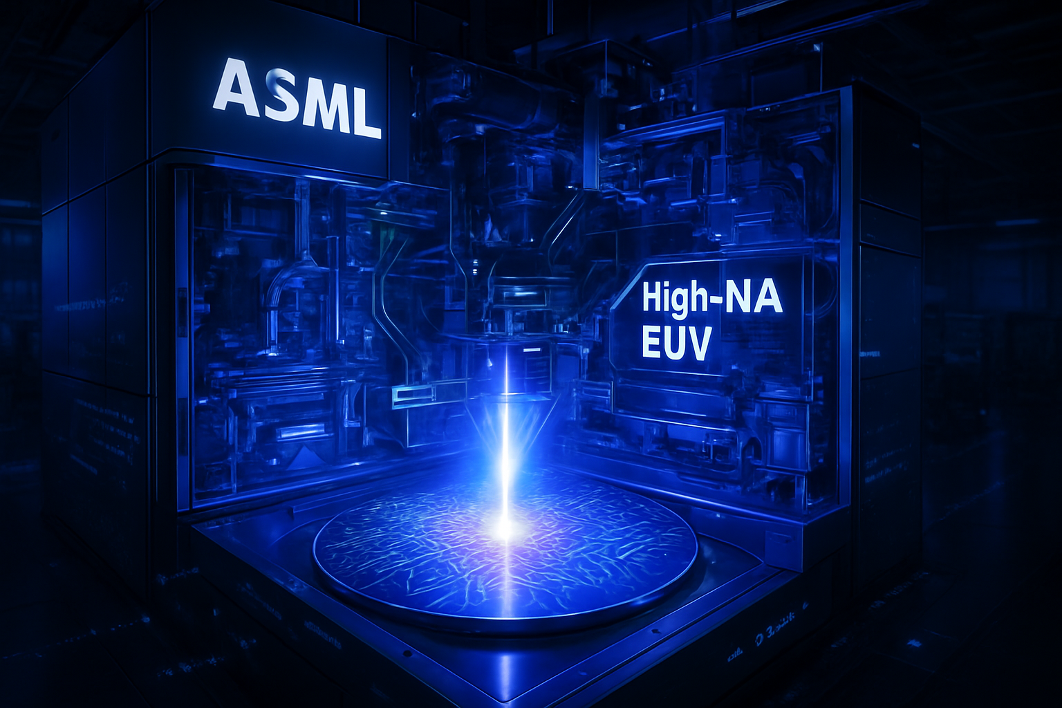
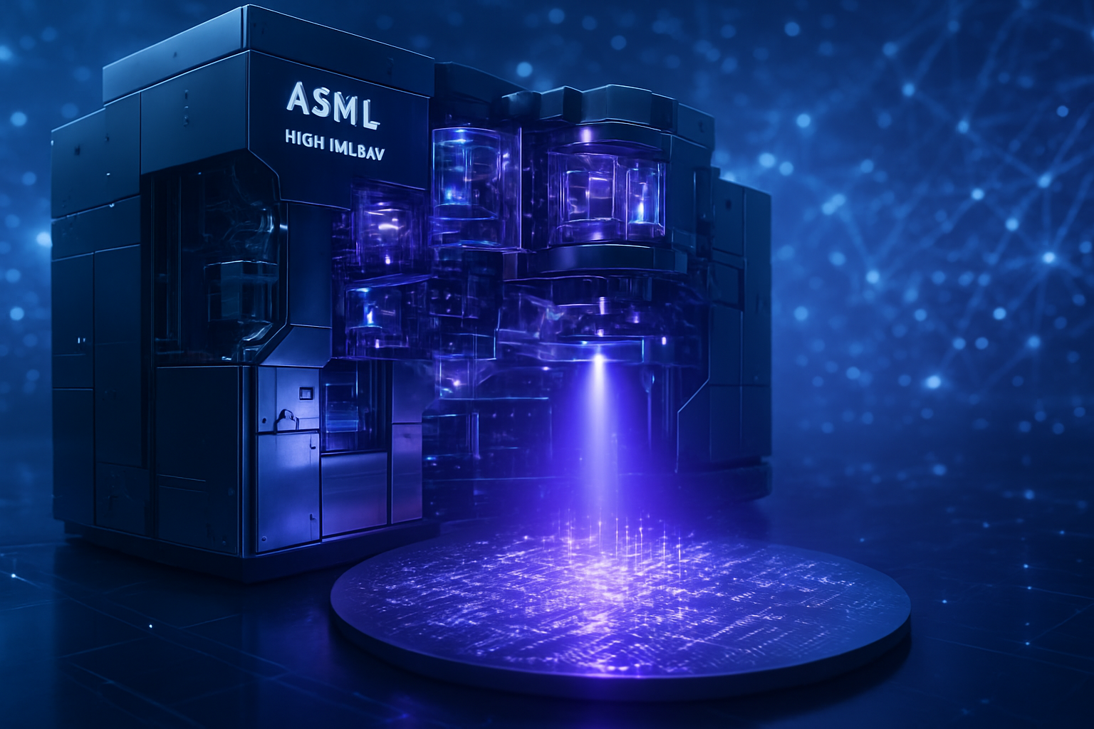
Tag: ASML

  • The Angstrom Era Begins: ASML’s High-NA EUV and the $380 Million Bet to Save Moore’s Law

    The Angstrom Era Begins: ASML’s High-NA EUV and the $380 Million Bet to Save Moore’s Law

    As of January 5, 2026, the semiconductor industry has officially entered the "Angstrom Era," a transition marked by the high-volume deployment of the most complex machine ever built: the High-Numerical Aperture (High-NA) Extreme Ultraviolet (EUV) lithography scanner. Developed by ASML (NASDAQ: ASML), the Twinscan EXE:5200B has become the defining tool for the sub-2nm generation of chips. This technological leap is not merely an incremental upgrade; it is the gatekeeper for the next decade of Moore’s Law, providing the precision necessary to print transistors at scales where atoms are the primary unit of measurement.

    The immediate significance of this development lies in the radical shift of the competitive landscape. Intel (NASDAQ: INTC), after a decade of trailing its rivals, has seized the "first-mover" advantage by becoming the first to integrate High-NA into its production lines. This aggressive stance is aimed directly at reclaiming the process leadership crown from TSMC (NYSE: TSM), which has opted for a more conservative, cost-optimized approach. As AI workloads demand exponentially more compute density and power efficiency, the success of High-NA EUV will dictate which silicon giants will power the next generation of generative AI models and hyperscale data centers.

    The Twinscan EXE:5200B: Engineering the Sub-2nm Frontier

    The technical specifications of the Twinscan EXE:5200B represent a paradigm shift in lithography. The "High-NA" designation refers to the increase in numerical aperture from 0.33 in standard EUV machines to 0.55. This change allows the machine to achieve a staggering 8nm resolution, enabling the printing of features approximately 1.7 times smaller than previous tools. In practical terms, this translates to a 2.9x increase in transistor density, allowing engineers to cram billions more gates onto a single piece of silicon without the need for the complex "multi-patterning" techniques that have plagued 3nm and 2nm yields.

    Beyond resolution, the EXE:5200B addresses the two most significant hurdles of early High-NA prototypes: throughput and alignment. The production-ready model now achieves a throughput of 175 to 200 wafers per hour (wph), matching the productivity of the latest low-NA scanners. Furthermore, it boasts an overlay accuracy of 0.7nm. This sub-nanometer precision is critical for a process known as "field stitching." Because High-NA optics halve the exposure field size, larger chips—such as the massive GPUs produced by NVIDIA (NASDAQ: NVDA)—must be printed in two separate halves. The 0.7nm overlay ensures these halves are aligned with such perfection that they function as a single, seamless monolithic die.

    This approach differs fundamentally from the industry's previous trajectory. For the past five years, foundries have relied on "multi-patterning," where a single layer is printed using multiple exposures to achieve finer detail. While effective, multi-patterning increases the risk of defects and significantly lengthens the manufacturing cycle. High-NA EUV returns the industry to "single-patterning" for the most critical layers, drastically simplifying the manufacturing flow and improving the "time-to-market" for cutting-edge designs. Initial reactions from the research community suggest that while the $380 million price tag per machine is daunting, the reduction in process steps and the jump in density make it an inevitable necessity for the sub-2nm era.

    A Tale of Two Strategies: Intel’s Leap vs. TSMC’s Caution

    The deployment of High-NA EUV has created a strategic schism between the world’s leading chipmakers. Intel has positioned itself as the "High-NA Vanguard," utilizing the EXE:5200B to underpin its 18A (1.8nm) and 14A (1.4nm) nodes. By early 2026, Intel's 18A process has reached high-volume manufacturing, with the first "Panther Lake" consumer chips hitting shelves. While 18A was designed to be compatible with standard EUV, Intel is selectively using High-NA tools to "de-risk" the technology before its 14A node becomes "High-NA native" later this year. This early adoption is a calculated risk to prove to foundry customers that Intel Foundry is once again the world's most advanced manufacturer.

    Conversely, TSMC has maintained a "wait-and-see" approach, focusing on optimizing its existing low-NA EUV infrastructure for its A14 (1.4nm) node. TSMC’s leadership has argued that the current cost-per-wafer for High-NA is too high for mass-market mobile chips, preferring to use multi-patterning on its ultra-mature NXE:3800E scanners. This creates a fascinating market dynamic: Intel is betting on technical superiority and process simplification to attract high-margin AI customers, while TSMC is betting on cost-efficiency and yield stability.

    The implications for the broader market are profound. If Intel successfully scales 14A using the EXE:5200B, it could potentially offer AI companies like AMD (NASDAQ: AMD) and even NVIDIA a performance-per-watt advantage that TSMC cannot match until its own High-NA transition, currently slated for 2027 or 2028. This disruption could shift the balance of power in the foundry business, which TSMC has dominated for over a decade. Startups specializing in "AI-first" silicon also stand to benefit, as the single-patterning capability of High-NA reduces the "design-to-chip" lead time, allowing for faster iteration of specialized neural processing units (NPUs).

    The Silicon Gatekeeper of the AI Revolution

    The significance of ASML’s High-NA dominance extends far beyond corporate rivalry; it is the physical foundation of the AI revolution. Modern Large Language Models (LLMs) are currently constrained by two factors: the amount of high-speed memory that can be placed near the compute units and the power efficiency of the data center. Sub-2nm chips produced with the EXE:5200B are expected to consume 25% to 35% less power for the same frequency compared to 3nm equivalents. In an era where electricity and cooling costs are the primary bottlenecks for AI scaling, these efficiency gains are worth billions to hyperscalers like Microsoft (NASDAQ: MSFT) and Google (NASDAQ: GOOGL).

    Furthermore, the transition to High-NA mirrors previous industry milestones, such as the initial shift from DUV to EUV in 2019. Just as that transition enabled the 5nm and 3nm chips that power today’s smartphones and AI accelerators, High-NA is the "second act" of EUV that will carry the industry toward the 1nm mark. However, the stakes are higher now. The geopolitical importance of semiconductor leadership has never been greater, and the "High-NA club" is currently an exclusive group. With ASML being the sole provider of these machines, the global supply chain for the most advanced AI hardware now runs through a single point of failure in Veldhoven, Netherlands.

    Potential concerns remain regarding the "halved field" issue. While field stitching has been proven in the lab, doing it at a scale of millions of units per month without impacting yield is a monumental challenge. If the stitching process leads to higher defect rates, the cost of the world’s most advanced AI GPUs could skyrocket, potentially slowing the democratization of AI compute. Nevertheless, the industry has historically overcome such lithographic hurdles, and the consensus is that High-NA is the only viable path forward.

    The Road to 14A and Beyond

    Looking ahead, the next 24 months will be critical for the validation of High-NA technology. Intel is expected to release its 14A Process Design Kit (PDK 1.0) to foundry customers in the coming months, which will be the first design environment built entirely around the capabilities of the EXE:5200B. This node will introduce "PowerDirect," a second-generation backside power delivery system that, when combined with High-NA lithography, promises a 20% performance boost over the already impressive 18A node.

    Experts predict that by 2028, the "High-NA gap" between Intel and TSMC will close as the latter finally integrates the tools into its "A14P" process. However, the "learning curve" advantage Intel is building today could prove difficult to overcome. We are also likely to see the emergence of "Hyper-NA" research—tools with numerical apertures even higher than 0.55—as the industry begins to look toward the sub-10-angstrom (sub-1nm) era in the 2030s. The immediate challenge for ASML and its partners will be to drive down the cost of these machines and improve the longevity of the specialized photoresists and masks required for such extreme resolutions.

    A New Chapter in Computing History

    The deployment of the ASML Twinscan EXE:5200B marks a definitive turning point in the history of computing. By enabling the mass production of sub-2nm chips, ASML has effectively extended the life of Moore’s Law at a time when many predicted its demise. Intel’s aggressive adoption of this technology represents a "moonshot" attempt to regain its former glory, while the industry’s shift toward "Angstrom-class" silicon provides the necessary hardware runway for the next decade of AI innovation.

    The key takeaways are clear: the EXE:5200B is the most productive and precise lithography tool ever created, Intel is currently the only player using it for high-volume manufacturing, and the future of AI hardware is now inextricably linked to the success of High-NA EUV. In the coming weeks and months, all eyes will be on Intel’s 18A yield reports and the first customer tape-outs for the 14A node. These metrics will serve as the first real-world evidence of whether the High-NA era will deliver on its promise of a new golden age for silicon.


    This content is intended for informational purposes only and represents analysis of current AI developments.

    TokenRing AI delivers enterprise-grade solutions for multi-agent AI workflow orchestration, AI-powered development tools, and seamless remote collaboration platforms.
    For more information, visit https://www.tokenring.ai/.

  • Silicon Sovereignty: Beijing’s 50% Domestic Mandate Reshapes the Global Semiconductor Landscape

    Silicon Sovereignty: Beijing’s 50% Domestic Mandate Reshapes the Global Semiconductor Landscape

    As of early 2026, the global semiconductor industry has reached a definitive tipping point. Beijing has officially, albeit quietly, weaponized its massive domestic market to force a radical decoupling from Western technology. The centerpiece of this strategy is a strictly enforced, unpublished mandate requiring that at least 50% of all semiconductor manufacturing equipment (SMEE) in new fabrication facilities be sourced from domestic vendors. This move marks the transition from "defensive self-reliance" to an aggressive pursuit of "Silicon Sovereignty," a doctrine that views total independence in chip production as the ultimate prerequisite for national security.

    The immediate significance of this policy cannot be overstated. By leveraging the state approval process for new fab capacity, China is effectively closing its doors to the "Big Three" equipment giants—Applied Materials (NASDAQ: AMAT), Lam Research (NASDAQ: LRCX), and ASML (NASDAQ: ASML)—unless they can navigate an increasingly narrow and regulated path. For the first time, the world’s largest market for semiconductor tools is no longer a level playing field, but a controlled environment designed to cultivate a 100% domestic supply chain. This shift is already causing a tectonic realignment in global capital flows, as investors grapple with the permanent loss of Chinese market share for Western firms.

    The Invisible Gatekeeper: Enforcement via Fab Capacity Permits

    The enforcement of this 50% mandate is a masterclass in bureaucratic precision. Unlike previous public subsidies or "Made in China 2025" targets, this rule remains unpublished to avoid direct challenges at the World Trade Organization (WTO). Instead, it is managed through the Ministry of Industry and Information Technology (MIIT) and provincial development commissions. Any firm seeking to break ground on a new fab or expand existing production lines must now submit a detailed procurement tender as a prerequisite for state approval. If the total value of domestic equipment—ranging from cleaning and etching tools to advanced deposition systems—falls below the 50% threshold, the permit is summarily denied or delayed indefinitely.

    Technically, this policy is supported by the massive influx of capital from Phase 3 of the National Integrated Circuit Industry Investment Fund, commonly known as the "Big Fund." Launched in 2024 with approximately $49 billion (344 billion yuan), Phase 3 has been laser-focused on the "bottleneck" technologies that previously prevented domestic fabs from meeting these quotas. While the MIIT allows for "strategic flexibility" in advanced nodes—granting temporary waivers for lithography tools that local firms cannot yet produce—the waivers are conditional. Fabs must present a "localization roadmap" that commits to replacing auxiliary foreign systems with domestic alternatives within 24 months of the fab’s commissioning.

    This approach differs fundamentally from previous industrial policies. Rather than just throwing money at R&D, Beijing is now creating guaranteed demand for local vendors. This "guaranteed market" allows Chinese equipment makers to iterate their hardware in high-volume manufacturing environments, a luxury they previously lacked when competing against established Western incumbents. Initial reactions from industry experts suggest that while this will inevitably lead to some inefficiencies and yield losses in the short term, the long-term effect will be the rapid maturation of the Chinese SMEE ecosystem.

    The Great Rebalancing: Global Giants vs. National Champions

    The impact on global equipment leaders has been swift and severe. Applied Materials (NASDAQ: AMAT) recently reported a projected revenue hit of over $700 million for the 2026 fiscal year, specifically citing the domestic mandate and tighter export curbs. AMAT’s China revenue share, which once sat comfortably above 35%, is expected to drop to approximately 29% by year-end. Similarly, Lam Research (NASDAQ: LRCX) is facing its most direct competition to date in the etching and deposition markets. As China’s self-sufficiency in etching tools has climbed toward 60%, Lam’s management has warned investors that China revenue will likely "normalize" at 30% or below for the foreseeable future.

    Even ASML (NASDAQ: ASML), which holds a near-monopoly on advanced lithography, is not immune. While the Dutch giant still provides the critical Extreme Ultraviolet (EUV) and advanced Deep Ultraviolet (DUV) systems that China cannot replicate, its legacy immersion DUV business is being cannibalized. The 50% mandate has forced Chinese fabs to prioritize local DUV alternatives for mature-node production, leading to a projected decline in ASML’s China sales from 45% of its total revenue in 2024 to just 25% by late 2026.

    Conversely, Naura Technology Group (SHE: 002371) has emerged as the primary beneficiary of this "Silicon Sovereignty" era. Now ranked 7th globally by market share, Naura is the first Chinese firm to break into the top 10. In 2025, the company saw a staggering 42% growth rate, fueled by the acquisition of key component suppliers and a record-breaking 779 patent filings. Naura is no longer just a low-cost alternative; it is now testing advanced plasma etching equipment on 7nm production lines at SMIC, effectively closing the technological gap with Lam Research and Applied Materials at a pace that few predicted two years ago.

    Geopolitical Fallout and the Rise of Two Tech Ecosystems

    This shift toward a 50% domestic mandate is the clearest signal yet that the global semiconductor industry is bifurcating into two distinct, non-interoperable ecosystems. The "Silicon Sovereignty" movement is not just about economics; it is a strategic decoupling intended to insulate China’s economy from future U.S.-led sanctions. By creating a 100% domestic supply chain for mature and mid-range nodes, Beijing ensures that its critical infrastructure—from automotive and telecommunications to industrial AI—can continue to function even under a total blockade of Western technology.

    This development mirrors previous milestones in the AI and tech landscape, such as the emergence of the "Great Firewall," but on a far more complex hardware level. Critics argue that this forced localization will lead to a "fragmented innovation" model, where global standards are replaced by regional silos. However, proponents of the move within China point to the rapid growth of domestic EDA (Electronic Design Automation) tools and RISC-V architecture as proof that a parallel ecosystem is not only possible but thriving. The concern for the West is that by dominating the mature-node market (28nm and above), China could eventually use its scale to drive down prices and push Western competitors out of the global market for "foundational" chips.

    The Road to 100%: What Lies Ahead

    Looking forward, the 50% mandate is likely just a stepping stone. Industry insiders predict that Beijing will raise the domestic requirement to 70% by 2028, with the ultimate goal of a 100% domestic supply chain by 2030. The primary hurdle remains lithography. While Chinese firms like SMEE are making strides in DUV, the complexity of EUV lithography remains a multi-year, if not multi-decade, challenge. However, the current strategy focuses on "good enough" technology for the vast majority of AI and industrial applications, rather than chasing the leading edge at any cost.

    In the near term, we can expect to see more aggressive acquisitions by Chinese firms to fill remaining gaps in the supply chain, particularly in Chemical Mechanical Polishing (CMP) and advanced metrology. The challenge for the international community will be how to respond to a market that is increasingly closed to foreign competition while simultaneously producing a surplus of mature-node chips for the global market. Experts predict that the next phase of this conflict will move from equipment mandates to "chip-dumping" investigations and retaliatory tariffs as the two ecosystems begin to clash in third-party markets.

    A New World Order in Semiconductors

    The 50% domestic mandate of 2026 will be remembered as the moment the "global" semiconductor industry died. In its place, we have a world defined by strategic autonomy and regional dominance. For China, the mandate has successfully catalyzed a domestic industry that was once decades behind, transforming firms like Naura into global powerhouses. For the West, it serves as a stark reminder that market access can be revoked as quickly as it was granted, necessitating a radical rethink of how companies like Applied Materials and ASML plan for long-term growth.

    As we move deeper into 2026, the industry should watch for the first "all-domestic" fab announcements, which are expected by the third quarter. These facilities will serve as the ultimate proof-of-concept for Silicon Sovereignty. The era of a unified global tech supply chain is over; the era of the semiconductor fortress has begun.


    This content is intended for informational purposes only and represents analysis of current AI and semiconductor developments.

    TokenRing AI delivers enterprise-grade solutions for multi-agent AI workflow orchestration, AI-powered development tools, and seamless remote collaboration platforms.
    For more information, visit https://www.tokenring.ai/.

  • The Fortress of Silicon: Europe’s Bold Pivot to Sovereign Chip Security Reshapes Global AI Trade

    The Fortress of Silicon: Europe’s Bold Pivot to Sovereign Chip Security Reshapes Global AI Trade

    As of January 2, 2026, the global semiconductor landscape has undergone a tectonic shift, driven by the European Union’s aggressive "Silicon Sovereignty" initiative. What began as a response to pandemic-era supply chain vulnerabilities has evolved into a comprehensive security-first doctrine. By implementing the first enforcement phase of the Cyber Resilience Act (CRA) and the revamped EU Chips Act 2.0, Brussels has effectively erected a "Silicon Shield," prioritizing the security and traceability of high-tech components over the raw volume of production. This movement is not merely about manufacturing; it is a fundamental reconfiguration of the global trade landscape, mandating that any silicon entering the European market meets stringent "Security-by-Design" standards that are now setting a new global benchmark.

    The immediate significance of this crackdown lies in its focus on the "hardware root of trust." Unlike previous decades where security was largely a software-level concern, the EU now legally mandates that microprocessors and sensors contain immutable security features at the silicon level. This has created a bifurcated global market: chips destined for Europe must undergo rigorous third-party assessments to earn a "CE" security mark, while less secure components are increasingly relegated to secondary markets. For the artificial intelligence industry, this means that the hardware running the next generation of LLMs and edge devices is becoming more transparent, more secure, and significantly more integrated into the European geopolitical sphere.

    Technically, the push for Silicon Sovereignty is anchored by the full operational status of five major "Pilot Lines" across the continent, coordinated by the Chips for Europe initiative. The NanoIC line at imec in Belgium is now testing sub-2nm architectures, while the FAMES line at CEA-Leti in France is pioneering Fully Depleted Silicon-on-Insulator (FD-SOI) technology. These advancements differ from previous approaches by moving away from general-purpose logic and toward specialized, energy-efficient "Green AI" hardware. The focus is on low-power inference at the edge, where security is baked into the physical gate architecture to prevent side-channel attacks and unauthorized data exfiltration—a critical requirement for the EU’s strict data privacy laws.

    The Cyber Resilience Act has introduced a technical mandate for "Active Vulnerability Reporting," requiring chipmakers to report exploited hardware flaws to the European Union Agency for Cybersecurity (ENISA) within 24 hours. This level of transparency is unprecedented in the semiconductor industry, which has traditionally guarded hardware errata as trade secrets. Industry experts from the AI research community have noted that these standards are forcing a shift from "black box" hardware to "verifiable silicon." By utilizing RISC-V open-source architectures for sovereign AI accelerators, European researchers are attempting to eliminate the "backdoor" risks often associated with proprietary instruction set architectures.

    Initial reactions from the industry have been a mix of praise for the enhanced security and concern over the cost of compliance. While the European Design Platform has successfully onboarded over 100 startups by providing low-barrier access to Electronic Design Automation (EDA) tools, the cost of third-party security audits for "Critical Class II" products—which include most AI-capable microprocessors—has added a significant layer of overhead. Nevertheless, the consensus among security experts is that this "Iron Curtain of Silicon" is a necessary evolution in an era where hardware-level vulnerabilities can compromise entire national infrastructures.

    This shift has created a new hierarchy among tech giants and specialized semiconductor firms. ASML Holding N.V. (NASDAQ: ASML) has emerged as the linchpin of this strategy, with the Dutch government fully aligning its export licenses for High-NA EUV lithography systems with the EU’s broader economic security goals. This alignment has effectively restricted the most advanced manufacturing capabilities to a "G7+ Chip Coalition," leaving competitors in non-aligned regions struggling to keep pace with the sub-2nm transition. Meanwhile, STMicroelectronics N.V. (NYSE: STM) and NXP Semiconductors N.V. (NASDAQ: NXPI) have seen their market positions bolstered as the primary providers of secure, automotive-grade AI chips that meet the new EU mandates.

    Intel Corporation (NASDAQ: INTC) has faced a more complex path; while its massive "Magdeburg" project in Germany saw delays throughout 2025, its Fab 34 in Leixlip, Ireland, has become the lead European hub for high-volume 3nm production. This has allowed Intel to position itself as a "sovereign-friendly" foundry for European AI startups like Mistral AI and Aleph Alpha. Conversely, Taiwan Semiconductor Manufacturing Company (NYSE: TSM) has had to adapt its European strategy, focusing heavily on specialized 12nm and 16nm nodes for the industrial and automotive sectors in its Dresden facility to satisfy the EU’s demand for local, secure supply chains for "Smart Power" applications.

    The competitive implications are profound for major AI labs. Companies that rely on highly centralized, non-transparent hardware may find themselves locked out of European government and critical infrastructure contracts. This has spurred a wave of strategic partnerships where software giants are co-designing hardware with European firms to ensure compliance. For instance, the integration of "Sovereign LLMs" directly onto NXP’s secure automotive platforms has become a blueprint for how AI companies can maintain a foothold in the European market by prioritizing local security standards over raw processing speed.

    Beyond the technical and corporate spheres, the "Silicon Sovereignty" movement represents a major milestone in the history of AI and global trade. It marks the end of the "borderless silicon" era, where components were designed in one country, manufactured in another, and packaged in a third with little regard for the geopolitical implications of the underlying hardware. This new era of "Technological Statecraft" mirrors the Cold War-era export controls but with a modern focus on AI safety and cybersecurity. The EU's move is a direct challenge to the dominance of both US-centric and China-centric supply chains, attempting to carve out a third way that prioritizes democratic values and data sovereignty.

    However, this fragmentation raises concerns about the "Balkanization" of the AI industry. If different regions mandate vastly different hardware security standards, the cost of developing global AI products could skyrocket. There is also the risk of a "security-performance trade-off," where the overhead required for real-time hardware monitoring and encrypted memory paths could make European-compliant chips slower or more expensive than their less-regulated counterparts. Comparisons are being made to the GDPR’s impact on the software industry; while initially seen as a burden, it eventually became a global gold standard that other regions felt compelled to emulate.

    The wider significance also touches on the environmental impact of AI. By focusing on "Green AI" and energy-efficient edge computing, Europe is attempting to lead the transition to a more sustainable AI infrastructure. The EU Chips Act’s support for Wide-Bandgap semiconductors, such as Silicon Carbide and Gallium Nitride, is a crucial part of this, enabling more efficient power conversion for the massive data centers required to train and run large-scale AI models. This "Green Sovereignty" adds a moral and environmental dimension to the geopolitical struggle for chip dominance.

    Looking ahead to the rest of 2026 and beyond, the next major milestone will be the full implementation of the Silicon Box (a €3.2B chiplet fab in Italy), which aims to bring advanced packaging capabilities back to European soil. This is critical because, until now, even chips designed and etched in Europe often had to be sent to Asia for the final "back-end" processing, creating a significant security gap. Once this facility is operational, the EU will possess a truly end-to-end sovereign supply chain for advanced AI chiplets.

    Experts predict that the focus will soon shift from logic chips to "Photonic Integrated Circuits" (PICs). The PIXEurope pilot line is expected to yield the first commercially viable light-based AI accelerators by 2027, which could offer a 10x improvement in energy efficiency for neural network processing. The challenge will be scaling these technologies and ensuring that the European ecosystem can attract enough high-tier talent to compete with the massive R&D budgets of Silicon Valley. Furthermore, the ongoing "Lithography War" will remain a flashpoint, as China continues to invest heavily in domestic alternatives to ASML’s technology, potentially leading to a complete decoupling of the global semiconductor market.

    In summary, Europe's crackdown on semiconductor security and its push for Silicon Sovereignty have fundamentally altered the trajectory of the AI industry. By mandating "Security-by-Design" and investing in a localized, secure supply chain, the EU has moved from a position of dependency to one of strategic influence. The key takeaways from this transition are the elevation of hardware security to a legal requirement, the rise of specialized "Green AI" architectures, and the emergence of a "G7+ Chip Coalition" that uses high-tech monopolies like High-NA EUV as diplomatic leverage.

    This development will likely be remembered as the moment when the geopolitical reality of AI hardware finally caught up with the borderless ambitions of AI software. As we move further into 2026, the industry must watch for the first wave of CRA-related enforcement actions and the progress of the "AI Factories" being built under the EuroHPC initiative. The "Fortress of Silicon" is now under construction, and its walls are being built with the dual bricks of security and sovereignty, forever changing how the world trades in the intelligence of the future.


    This content is intended for informational purposes only and represents analysis of current AI developments.

    TokenRing AI delivers enterprise-grade solutions for multi-agent AI workflow orchestration, AI-powered development tools, and seamless remote collaboration platforms.
    For more information, visit https://www.tokenring.ai/.

  • High-NA EUV: Intel and ASML Push the Limits of Physics with Sub-2nm Lithography

    High-NA EUV: Intel and ASML Push the Limits of Physics with Sub-2nm Lithography

    Intel has officially claimed a decisive first-mover advantage in the burgeoning "Angstrom Era" by announcing the successful completion of acceptance testing for ASML’s Twinscan EXE:5200B High-NA EUV machines. This milestone, achieved at Intel’s D1X facility in Oregon, marks the transition of High-Numerical Aperture (High-NA) lithography from a research-and-development curiosity into a high-volume manufacturing (HVM) reality. As the semiconductor industry enters 2026, this development positions Intel as the vanguard in the race to produce sub-2nm chips, which are expected to power the next generation of generative AI and high-performance computing.

    The significance of this achievement cannot be overstated. By validating the EXE:5200B, Intel (Nasdaq: INTC) has secured the hardware foundation necessary for its "14A" (1.4nm) process node. These $380 million systems represent the most complex machines ever built for commercial use, utilizing a higher numerical aperture of 0.55 to print features as small as 8nm. This is nearly twice the resolution of standard Extreme Ultraviolet (EUV) lithography, providing Intel with a critical window of opportunity to regain the process leadership it lost over the previous decade.

    The Physics of the Angstrom Era: 0.55 NA and Anamorphic Optics

    The jump from standard EUV (0.33 NA) to High-NA (0.55 NA) is a fundamental shift in optical physics rather than a simple incremental upgrade. In lithography, the Rayleigh criterion dictates that the minimum feature size is inversely proportional to the numerical aperture. By increasing the NA to 0.55, ASML (Nasdaq: ASML) has enabled a 1.7x improvement in resolution and a nearly 2.9x increase in transistor density. This allows for the printing of features that were previously impossible to resolve in a single pass, effectively extending the roadmap for Moore’s Law into the 2030s.

    Technically, the EXE:5200B achieves this through the use of anamorphic optics—mirrors that magnify the X and Y axes differently (4x and 8x magnification). While this design allows for higher resolution without requiring massive increases in mask size, it introduces a "half-field" exposure limitation. Large chips, such as the massive AI accelerators produced by companies like Nvidia (Nasdaq: NVDA), must now be printed in two halves and "stitched" together with sub-nanometer precision. Intel’s successful acceptance testing confirms that it has mastered this "field stitching" process, achieving an overlay accuracy of 0.7nm.

    The primary manufacturing advantage of High-NA is the return to "single-patterning." In recent years, chipmakers have been forced to use "multi-patterning"—multiple exposures for a single layer—to push standard EUV tools beyond their native resolution. Multi-patterning is notoriously complex, requiring more masks and significantly longer manufacturing cycles. By using High-NA for critical layers, Intel can print the densest features in a single exposure, drastically reducing manufacturing complexity, shortening cycle times, and potentially improving yields for its most advanced 1.4nm designs.

    A High-Stakes Gamble: Intel vs. TSMC and Samsung

    Intel’s aggressive adoption of High-NA EUV is a calculated gamble that sets it apart from its primary rivals. While Intel is moving full steam ahead with the EXE:5200B for its 14A node, Taiwan Semiconductor Manufacturing Company (NYSE: TSM) has taken a more conservative "wait-and-see" approach. TSMC has publicly stated that it will likely skip High-NA for its initial A14 (1.4nm) node, opting instead to push standard EUV tools to their absolute limits through advanced multi-patterning. TSMC’s strategy prioritizes cost-efficiency and the use of mature tools, betting that the high capital expenditure of High-NA ($380M+ per machine) is not yet economically justified.

    Samsung, meanwhile, is occupying the middle ground. The South Korean giant has secured its own EXE:5200B systems for early 2026, intending to use the technology for its 2nm (SF2) and sub-2nm logic processes, as well as for advanced DRAM and HBM4 (High Bandwidth Memory). By integrating High-NA into its memory production, Samsung hopes to gain an edge in the AI hardware market, where memory bandwidth is often the primary bottleneck for large language models.

    The competitive implications are stark. If Intel can successfully scale its 14A node with High-NA, it could offer a transistor density and power-efficiency advantage that TSMC cannot match with standard EUV. However, the "economic crossover" point is narrow; analysts suggest that High-NA only becomes cheaper than standard EUV when it replaces three or more Low-NA exposures. Intel’s success depends on whether the performance gains of 14A can command a high enough premium from customers like Microsoft (Nasdaq: MSFT) and Amazon (Nasdaq: AMZN) to offset the staggering cost of the ASML hardware.

    Beyond Moore’s Law: The Broader Impact on AI and Geopolitics

    The transition to High-NA EUV is not just a corporate milestone; it is a pivotal moment for the entire AI landscape. The most advanced AI models today are limited by the physical constraints of the hardware they run on. Sub-2nm chips will allow for significantly more transistors on a single die, enabling the creation of AI accelerators with higher throughput, lower power consumption, and more integrated memory. This is essential for the "Scale-Out" phase of AI, where the goal is to move from training massive models in data centers to running sophisticated, agentic AI on edge devices and smartphones.

    From a geopolitical perspective, the successful deployment of High-NA EUV in the United States represents a major win for the CHIPS Act and domestic semiconductor manufacturing. By hosting the world’s first production-ready High-NA fleet at its Oregon facility, Intel is positioning the U.S. as a hub for the most advanced lithography on the planet. This has profound implications for national security and supply chain resilience, as the world’s most advanced AI silicon will no longer be solely dependent on fabrication facilities in East Asia.

    However, the shift also raises concerns about the widening "compute divide." The extreme cost of High-NA lithography means that only the largest, most well-funded companies will be able to afford the chips produced on these nodes. This could further centralize the power of AI development in the hands of a few tech giants, as startups and smaller research labs find themselves priced out of the most advanced silicon.

    The Roadmap Ahead: Risk Production and Hyper-NA

    Looking forward, the immediate focus for Intel will be the release of its 14A Process Design Kit (PDK) 1.0 to foundry customers. Risk production for the 14A node is expected to begin in late 2026 or early 2027, with high-volume manufacturing targeted for 2028. During this period, the industry will be watching closely to see if Intel can maintain high yields while managing the complexities of anamorphic optics and half-field stitching.

    Beyond 1.4nm, the industry is already looking toward the 1nm (10A) node and the potential for "Hyper-NA" lithography. ASML is reportedly exploring systems with an NA higher than 0.7, which would require even more radical changes to lens design and photoresist chemistry. While Hyper-NA is likely a decade away, the successful implementation of High-NA today proves that the industry is still capable of overcoming the "impossible" barriers of physics to keep the digital revolution moving forward.

    Conclusion: A New Chapter in Silicon History

    The completion of acceptance testing for the ASML Twinscan EXE:5200B is a watershed moment that officially kicks off the Angstrom Era. Intel’s willingness to embrace the risks and costs of High-NA EUV has allowed it to leapfrog its competitors in hardware readiness, setting the stage for a dramatic showdown in the sub-2nm market. Whether this technical lead translates into market dominance remains to be seen, but the achievement itself is a testament to the incredible engineering prowess of both Intel and ASML.

    In the coming months, the industry will be looking for the first test chips to emerge from the 14A process. These early results will provide the first real-world data on whether High-NA can deliver on its promise of superior density and efficiency. For now, the limits of physics have once again been pushed back, ensuring that the exponential growth of AI and computing power will continue into the next decade.


    This content is intended for informational purposes only and represents analysis of current AI developments.

    TokenRing AI delivers enterprise-grade solutions for multi-agent AI workflow orchestration, AI-powered development tools, and seamless remote collaboration platforms.
    For more information, visit https://www.tokenring.ai/.

  • The Silicon Curtain Descends: China Unveils Shenzhen EUV Prototype in ‘Manhattan Project’ Breakthrough

    The Silicon Curtain Descends: China Unveils Shenzhen EUV Prototype in ‘Manhattan Project’ Breakthrough

    As the calendar turns to 2026, the global semiconductor landscape has been fundamentally reshaped by a seismic announcement from Shenzhen. Reports have confirmed that a high-security research facility in China’s technology hub has successfully operated a functional Extreme Ultraviolet (EUV) lithography prototype. Developed under a state-mandated "whole-of-nation" effort often referred to as the "Chinese Manhattan Project," this breakthrough marks the first time a domestic Chinese entity has solved the fundamental physics of EUV light generation—a feat previously thought to be a decade away.

    The emergence of this operational machine, which reportedly utilizes a novel Laser-Induced Discharge Plasma (LDP) light source, signals a direct challenge to the Western monopoly on leading-edge chipmaking. For years, the Dutch firm ASML Holding N.V. (NASDAQ:ASML) has been the sole provider of EUV tools, which are essential for producing chips at 7nm and below. By achieving this milestone, China has effectively punctured the "hard ceiling" of Western export controls, setting an aggressive roadmap to reach 2nm parity by 2028 and threatening to bifurcate the global technology ecosystem into two distinct, non-interoperable stacks.

    Breaking the Light Barrier: The LDP Innovation

    The Shenzhen prototype represents a significant departure from the industry-standard architecture pioneered by ASML. While ASML’s machines rely on Laser-Produced Plasma (LPP)—where high-power $CO_2$ lasers vaporize tin droplets 50,000 times per second—the Chinese system utilizes Laser-Induced Discharge Plasma (LDP). Developed by a consortium led by the Harbin Institute of Technology (HIT) and the Shanghai Institute of Optics and Fine Mechanics (SIOM), the LDP source uses a solid-state laser to vaporize tin, followed by a high-voltage discharge to create the plasma. This approach is technically distinct and avoids many of the specific patents held by Western firms, though it currently requires a much larger physical footprint, with the prototype reportedly filling an entire factory floor.

    Technical specifications leaked from the Shenzhen facility indicate that the machine has achieved a stable 13.5nm EUV beam with a conversion efficiency of 3.42%. While this is still below the 5% to 6% efficiency required for high-volume commercial throughput, it is a massive leap from previous experimental results. The light source is currently outputting between 100W and 150W, with engineers targeting 250W for a production-ready model. The project has been bolstered by a "human intelligence" campaign that successfully recruited dozens of former ASML engineers, including high-ranking specialists like Lin Nan, who reportedly filed multiple EUV patents under an alias at SIOM after leaving the Dutch giant.

    Initial reactions from the semiconductor research community have been a mix of skepticism and alarm. Experts at the Interuniversity Microelectronics Centre (IMEC) note that while the physics of the light source have been validated, the immense challenge of precision optics remains. China’s Changchun Institute of Optics, Fine Mechanics and Physics (CIOMP) is tasked with developing the objective lens assembly and interferometers required to focus that light with sub-nanometer accuracy. Industry insiders suggest that while the machine is not yet ready for mass production, it serves as a "proof of concept" that justifies the billions of dollars in state subsidies poured into the project over the last three years.

    Market Shockwaves and the Rise of the 'Sovereign Stack'

    The confirmation of the Shenzhen prototype has sent shockwaves through the executive suites of Silicon Valley and Hsinchu. Huawei Technologies, the primary coordinator and financier of the project, stands to be the biggest beneficiary. By integrating this domestic EUV tool into its Dongguan testing facilities, Huawei aims to secure a "sovereign supply chain" that is immune to US Department of Commerce sanctions. This development directly benefits Shenzhen-based startups like SiCarrier Technologies, which provides the critical etching and metrology tools needed to complement the EUV system, and SwaySure Technology, a Huawei-linked firm focused on domestic DRAM production.

    For global giants like Intel Corporation (NASDAQ:INTC) and Taiwan Semiconductor Manufacturing Company (NYSE:TSM), the breakthrough accelerates an already frantic arms race. Intel has doubled down on its "first-mover" advantage with ASML’s next-generation High-NA EUV machines, aiming to launch its 1.4nm (14A) node by late 2026 to maintain a technological "moat." Meanwhile, TSMC has reportedly accelerated its A16 and A14 roadmaps, realizing that their "Silicon Shield" now depends on maintaining a permanent two-generation lead rather than a monopoly on the equipment itself. The market positioning of ASML has also been called into question, with its stock experiencing volatility as investors price in the eventual loss of the Chinese market, which previously accounted for a significant portion of its DUV (Deep Ultraviolet) revenue.

    The strategic advantage for China lies in its ability to ignore commercial margins in favor of national security. While an ASML EUV machine costs upwards of $200 million and must be profitable for a commercial fab, the Chinese "Manhattan Project" is state-funded. This allows Chinese fabs to operate at lower yields and higher costs, provided they can produce the 5nm and 3nm chips required for domestic AI accelerators like the Huawei Ascend series. This shift threatens to disrupt the existing service-based revenue models of Western toolmakers, as China moves toward a "100% domestic content" mandate for its internal chip industry.

    Global Reshoring and the 'Silicon Curtain'

    The Shenzhen breakthrough is the most significant milestone in the semiconductor industry since the invention of the transistor, signaling the end of the unified global supply chain. It fits into a broader trend of "Global Reshoring," where national governments are treating chip production as a critical utility rather than a globalized commodity. The US Department of Commerce, led by Under Secretary Howard Lutnick, has responded by moving from "selective restrictions" to "structural containment," recently revoking the "validated end-user" status for foreign-owned fabs in China to prevent the leakage of spare parts into the domestic EUV program.

    This development effectively lowers a "Silicon Curtain" between the East and West. On one side is the Western "High-NA" stack, led by the US, Japan, and the Netherlands, focused on high-efficiency, market-driven, leading-edge nodes. On the other is the Chinese "Sovereign" stack, characterized by state-subsidized resilience and a "good enough" philosophy for domestic AI and military applications. The potential concern for the global economy is the creation of two non-interoperable tech ecosystems, which could lead to redundant R&D costs, incompatible AI standards, and a fragmented market for consumer electronics.

    Comparisons to previous AI milestones, such as the release of GPT-4, are apt; while GPT-4 was a breakthrough in software and data, the Shenzhen EUV prototype is the hardware equivalent. It is the physical foundation upon which China’s future AI ambitions rest. Without domestic EUV, China would eventually be capped at 7nm or 5nm using multi-patterning DUV, which is prohibitively expensive and inefficient. With EUV, the path to 2nm and beyond—the "holy grail" of current semiconductor physics—is finally open to them.

    The Road to 2nm: 2028 and Beyond

    Looking ahead, the next 24 months will be critical for the refinement of the Shenzhen prototype. Near-term developments will likely focus on increasing the power of the LDP light source to 250W and improving the reliability of the vacuum systems. Analysts expect the first "EUV-refined" 5nm chips to roll out of Huawei’s Dongguan facility by late 2026, serving as a pilot run for more complex architectures. The ultimate goal remains 2nm parity by 2028, a target that would bring China within striking distance of the global leading edge.

    However, significant challenges remain. Lithography is only one part of the puzzle; China must also master advanced packaging, photoresist chemistry, and high-purity gases—all of which are currently subject to heavy export controls. Experts predict that China will continue to use "shadow supply chains" and domestic innovation to fill these gaps. We may also see the development of alternative paths, such as Steady-State Micro-Bunching (SSMB) particle accelerators, which Beijing is exploring as a way to provide EUV light to entire clusters of lithography machines at once, potentially leapfrogging the throughput of individual ASML units.

    The most immediate application for these domestic EUV chips will be in AI training and inference. As Nvidia Corporation (NASDAQ:NVDA) faces tightening restrictions on its exports to China, the pressure on Huawei to produce a 5nm or 3nm Ascend chip becomes an existential necessity for the Chinese AI industry. If the Shenzhen prototype can be successfully scaled, it will provide the compute power necessary for China to remain a top-tier player in the global AI race, regardless of Western sanctions.

    A New Era of Technological Sovereignty

    The successful operation of the Shenzhen EUV prototype is a watershed moment that marks the transition from a world of technological interdependence to one of technological sovereignty. The key takeaway is that the "unsolvable" problem of EUV lithography has been solved by a second global power, albeit through a different and more resource-intensive path. This development validates China’s "whole-of-nation" approach to science and technology and suggests that financial and geopolitical barriers can be overcome by concentrated state power and strategic talent acquisition.

    In the context of AI history, this will likely be remembered as the moment the hardware bottleneck was broken for the world’s second-largest economy. The long-term impact will be a more competitive, albeit more divided, global tech landscape. While the West continues to lead in absolute performance through High-NA EUV and 1.4nm nodes, the "performance gap" that sanctions were intended to maintain is narrowing faster than anticipated.

    In the coming weeks and months, watch for official statements from the Chinese Ministry of Industry and Information Technology (MIIT) regarding the commercialization roadmap for the "Famous Mountain" suite of tools. Simultaneously, keep a close eye on the US Department of Commerce for further "choke point" restrictions aimed at the LDP light source components. The era of the unified global chip is over; the era of the sovereign silicon stack has begun.


    This content is intended for informational purposes only and represents analysis of current AI and semiconductor developments as of January 1, 2026.

    TokenRing AI delivers enterprise-grade solutions for multi-agent AI workflow orchestration, AI-powered development tools, and seamless remote collaboration platforms. For more information, visit https://www.tokenring.ai/.

  • The Dawn of the Angstrom Era: Intel Claims First-Mover Advantage as ASML’s High-NA EUV Enters High-Volume Manufacturing

    The Dawn of the Angstrom Era: Intel Claims First-Mover Advantage as ASML’s High-NA EUV Enters High-Volume Manufacturing

    As of January 1, 2026, the semiconductor industry has officially crossed the threshold into the "Angstrom Era," marking a pivotal shift in the global race for silicon supremacy. The primary catalyst for this transition is the full-scale rollout of High-Numerical Aperture (High-NA) Extreme Ultraviolet (EUV) lithography. Leading the charge, Intel Corporation (NASDAQ: INTC) recently announced the successful completion of acceptance testing for its first fleet of ASML (NASDAQ: ASML) Twinscan EXE:5200B machines. This milestone signals that the world’s most advanced manufacturing equipment is no longer just an R&D experiment but is now ready for high-volume manufacturing (HVM).

    The immediate significance of this development cannot be overstated. By successfully integrating High-NA EUV, Intel has positioned itself to regain the process leadership it lost over a decade ago. The ability to print features at the sub-2nm level—specifically targeting the Intel 14A (1.4nm) node—provides a direct path to creating the ultra-dense, energy-efficient chips required to power the next generation of generative AI models and hyperscale data centers. While competitors have been more cautious, Intel’s "all-in" strategy on High-NA has created a temporary but significant technological moat in the high-stakes foundry market.

    The Technical Leap: 0.55 NA and Anamorphic Optics

    The technical leap from standard EUV to High-NA EUV is defined by a move from a numerical aperture of 0.33 to 0.55. This increase in NA allows for a much higher resolution, moving from the 13nm limit of previous machines down to a staggering 8nm. In practical terms, this allows chipmakers to print features that are nearly twice as small without the need for complex "multi-patterning" techniques. Where standard EUV required two or three separate exposures to define a single layer at the sub-2nm level, High-NA EUV enables "single-patterning," which drastically reduces process complexity, shortens production cycles, and theoretically improves yields for the most advanced transistors.

    To achieve this 0.55 NA without making the internal mirrors impossibly large, ASML and its partner ZEISS developed a revolutionary "anamorphic" optical system. These optics provide different magnifications in the X and Y directions (4x and 8x respectively), resulting in a "half-field" exposure size. Because the machine only scans half the area of a standard exposure at once, ASML had to significantly increase the speed of the wafer and reticle stages to maintain high productivity. The current EXE:5200B models are now hitting throughput benchmarks of 175 to 220 wafers per hour, matching the productivity of older systems while delivering vastly superior precision.

    This differs from previous approaches primarily in its handling of the "resolution limit." As chips approached the 2nm mark, the industry was hitting a physical wall where the wavelength of light used in standard EUV was becoming too coarse for the features being printed. The industry's initial reaction was skepticism regarding the cost and the half-field challenge, but as the first production wafers from Intel’s D1X facility in Oregon show, the transition to 0.55 NA has proven to be the only viable path to sustaining the density improvements required for 1.4nm and beyond.

    Industry Impact: A Divergence in Strategy

    The rollout of High-NA EUV has created a stark divergence in the strategies of the world’s "Big Three" chipmakers. Intel has leveraged its first-mover advantage to attract high-profile customers for its Intel Foundry services, releasing the 1.4nm Process Design Kit (PDK) to major players like Nvidia (NASDAQ: NVDA) and Microsoft (NASDAQ: MSFT). By being the first to master the EXE:5200 platform, Intel is betting that it can offer a more streamlined and cost-effective production route for AI hardware than its rivals, who must rely on expensive multi-patterning with older machines to reach similar densities.

    Conversely, Taiwan Semiconductor Manufacturing Company (NYSE: TSM), the world's largest foundry, has maintained a more conservative "wait-and-see" approach. TSMC’s leadership has argued that the €380 million ($400 million USD) price tag per High-NA machine is currently too high to justify for its A16 (1.6nm) node. Instead, TSMC is maximizing its existing 0.33 NA fleet, betting that its superior manufacturing maturity will outweigh Intel’s early adoption of new hardware. However, with Intel now demonstrating operational HVM capability, the pressure on TSMC to accelerate its own High-NA timeline for its upcoming A14 and A10 nodes has intensified significantly.

    Samsung Electronics (KRX: 005930) occupies the middle ground, having taken delivery of its first production-grade EXE:5200B in late 2025. Samsung is targeting the technology for its 2nm Gate-All-Around (GAA) process and its next-generation DRAM. This strategic positioning allows Samsung to stay within striking distance of Intel while avoiding some of the "bleeding edge" risks associated with being the very first to deploy the technology. The market positioning is clear: Intel is selling "speed to market" for the most advanced nodes, while TSMC and Samsung are focusing on "cost-efficiency" and "proven reliability."

    Wider Significance: Sustaining Moore's Law in the AI Era

    The broader significance of the High-NA rollout lies in its role as the life support system for Moore’s Law. For years, critics have predicted the end of exponential scaling, citing the physical limits of silicon. High-NA EUV provides a clear roadmap for the next decade, enabling the industry to look past 2nm toward 1.4nm, 1nm, and even sub-1nm (angstrom) architectures. This is particularly critical in the current AI-driven landscape, where the demand for compute power is doubling every few months. Without the density gains provided by High-NA, the power consumption and physical footprint of future AI data centers would become unsustainable.

    However, this transition also raises concerns regarding the further centralization of the semiconductor supply chain. With each machine costing nearly half a billion dollars and requiring specialized facilities, the barrier to entry for advanced chip manufacturing has never been higher. This creates a "winner-take-most" dynamic where only a handful of companies—and by extension, a handful of nations—can participate in the production of the world’s most advanced technology. The geopolitical implications are profound, as the possession of High-NA capability becomes a matter of national economic security.

    Compared to previous milestones, such as the initial introduction of EUV in 2019, the High-NA rollout has been more technically challenging but arguably more critical. While standard EUV was about making existing processes easier, High-NA is about making the "impossible" possible. It represents a fundamental shift in how we think about the limits of lithography, moving from simple scaling to a complex dance of anamorphic optics and high-speed mechanical precision.

    Future Outlook: The Path to 1nm and Beyond

    Looking ahead, the next 24 months will be focused on the transition from "risk production" to "high-volume manufacturing" for the 1.4nm node. Intel expects its 14A process to be the primary driver of its foundry revenue by 2027, while the industry as a whole begins to look toward the next evolution of the technology: "Hyper-NA." ASML is already in the early stages of researching machines with an NA higher than 0.75, which would be required to reach the 0.5nm level by the 2030s.

    In the near term, the most significant application of High-NA EUV will be in the production of next-generation AI accelerators and mobile processors. We can expect the first consumer devices featuring 1.4nm chips—likely high-end smartphones and AI-integrated laptops—to hit the shelves by late 2027 or early 2028. The challenge remains the steep learning curve; mastering the half-field stitching and the new photoresist chemistries required for such small features will likely lead to some initial yield volatility as the technology matures.

    Conclusion: A Milestone in Silicon History

    In summary, the successful deployment and acceptance of the ASML Twinscan EXE:5200B at Intel marks the beginning of a new chapter in semiconductor history. Intel’s early lead in High-NA EUV has disrupted the established hierarchy of the foundry market, forcing competitors to re-evaluate their roadmaps. While the costs are astronomical, the reward is the ability to print the most complex structures ever devised by humanity, enabling a future of AI and high-performance computing that was previously unimaginable.

    As we move further into 2026, the key metrics to watch will be the yield rates of Intel’s 14A node and the speed at which TSMC and Samsung move to integrate their own High-NA fleets. The "Angstrom Era" is no longer a distant vision; it is a physical reality currently being etched into silicon in the cleanrooms of Oregon, South Korea, and Taiwan. The race to 1nm has officially begun.


    This content is intended for informational purposes only and represents analysis of current AI and semiconductor developments.

    TokenRing AI delivers enterprise-grade solutions for multi-agent AI workflow orchestration, AI-powered development tools, and seamless remote collaboration platforms.
    For more information, visit https://www.tokenring.ai/.

  • Intel Seizes Manufacturing Crown: World’s First High-NA EUV Production Line Hits 30,000 Wafers per Quarter for 18A Node

    Intel Seizes Manufacturing Crown: World’s First High-NA EUV Production Line Hits 30,000 Wafers per Quarter for 18A Node

    In a move that signals a seismic shift in the global semiconductor landscape, Intel (NASDAQ: INTC) has officially transitioned its most advanced manufacturing process into high-volume production. By successfully processing 30,000 wafers per quarter using the world’s first High-NA (Numerical Aperture) Extreme Ultraviolet (EUV) lithography machines, the company has reached a critical milestone for its 18A (1.8nm) process node. This achievement represents the first time these $380 million machines, manufactured by ASML (NASDAQ: ASML), have been utilized at such a scale, positioning Intel as the current technological frontrunner in the race to sub-2nm chip manufacturing.

    The significance of this development cannot be overstated. For nearly a decade, Intel struggled to maintain its lead against rivals like TSMC (NYSE: TSM) and Samsung (KRX: 005930), but the aggressive adoption of High-NA EUV technology appears to be the "silver bullet" the company needed. By hitting the 30,000-wafer mark as of late 2025, Intel is not just testing prototypes; it is proving that the most complex manufacturing equipment ever devised by humanity is ready for the demands of the AI-driven global economy.

    Technical Breakthrough: The Power of 0.55 NA

    The technical backbone of this milestone is the ASML Twinscan EXE:5200, a machine that stands as a marvel of modern physics. Unlike standard EUV machines that utilize a 0.33 Numerical Aperture, High-NA EUV increases this to 0.55. This allows for a significantly finer focus of the EUV light, enabling the printing of features as small as 8nm in a single exposure. In previous generations, achieving such tiny dimensions required "multi-patterning," a process where a single layer of a chip is passed through the machine multiple times. Multi-patterning is notoriously expensive, time-consuming, and prone to alignment errors that can ruin an entire wafer of chips.

    By moving to single-exposure 8nm printing, Intel has effectively slashed the complexity of its manufacturing flow. Industry experts note that High-NA EUV can reduce the number of processing steps for critical layers by nearly 50%, which theoretically leads to higher yields and faster production cycles. Furthermore, the 18A node introduces two other foundational technologies: RibbonFET (Intel’s implementation of Gate-All-Around transistors) and PowerVia (a revolutionary backside power delivery system). While RibbonFET improves transistor performance, PowerVia solves the "wiring bottleneck" by moving power lines to the back of the silicon, leaving more room for data signals on the front.

    Initial reactions from the AI research community and semiconductor analysts have been cautiously optimistic. While TSMC has historically been more conservative, opting to stick with older Low-NA machines for its 2nm (N2) node to save costs, Intel’s "all-in" gamble on High-NA is being viewed as a high-risk, high-reward strategy. If Intel can maintain stable yields at 30,000 wafers per quarter, it will have a clear path to reclaiming the "process leadership" title it lost in the mid-2010s.

    Industry Disruption: A New Challenger for AI Silicon

    The implications for the broader tech industry are profound. For years, the world’s leading AI labs and hardware designers—including NVIDIA (NASDAQ: NVDA), Apple (NASDAQ: AAPL), and AMD (NASDAQ: AMD)—have been almost entirely dependent on TSMC for their most advanced silicon. Intel’s successful ramp-up of the 18A node provides a viable second source for high-performance AI chips, which could lead to more competitive pricing and a more resilient global supply chain.

    For Intel Foundry, this is a "make or break" moment. The company is positioning itself to become the world’s second-largest foundry by 2030, and the 18A node is its primary lure for external customers. Microsoft (NASDAQ: MSFT) has already signed on as a major customer for the 18A process, and other tech giants are reportedly monitoring Intel’s yield rates closely. If Intel can prove that High-NA EUV provides a cost-per-transistor advantage over TSMC’s multi-patterning approach, we could see a significant migration of chip designs toward Intel’s domestic Fabs in Arizona and Ohio.

    However, the competitive landscape remains fierce. While Intel leads in the adoption of High-NA, TSMC’s N2 node is expected to be extremely mature and high-yielding by 2026. The market positioning now comes down to a battle between Intel’s architectural innovation (High-NA + PowerVia) and TSMC’s legendary manufacturing consistency. For startups and smaller AI companies, Intel's emergence as a top-tier foundry could provide easier access to cutting-edge silicon that was previously reserved for the industry's largest players.

    Geopolitical and Scientific Significance

    Looking at the wider significance, the success of the 18A node is a testament to the continued survival of Moore’s Law. Many critics argued that as we approached the 1nm limit, the physical and financial hurdles would become insurmountable. Intel’s 30,000-wafer milestone proves that through massive capital investment and international collaboration—specifically between the US-based Intel and the Netherlands-based ASML—the industry can continue to scale.

    This development also carries heavy geopolitical weight. As the US government continues to push for domestic semiconductor self-sufficiency through the CHIPS Act, Intel’s Fab 52 in Arizona has become a symbol of American industrial resurgence. The ability to produce the world’s most advanced AI processors on US soil reduces reliance on East Asian supply chains, which are increasingly seen as a point of strategic vulnerability.

    Comparatively, this milestone mirrors the transition to EUV lithography nearly a decade ago. At that time, those who adopted EUV early (like TSMC) gained a massive advantage, while those who delayed (like Intel) fell behind. By being the first to cross the High-NA finish line, Intel is attempting to flip the script, forcing its competitors to play catch-up with a technology that costs nearly $400 million per machine and requires a complete overhaul of fab logistics.

    The Road to 1nm: What Lies Ahead

    Looking ahead, the near-term focus for Intel will be the full-scale launch of "Panther Lake" and "Clearwater Forest"—the first internal products to utilize the 18A node. These chips are expected to hit the market in early 2026, serving as the ultimate test of the 18A process in real-world AI PC and server environments. If these products perform as expected, the next step will be the 14A node, which is designed to be "High-NA native" from the ground up.

    The long-term roadmap involves scaling toward the 10A (1nm) node by the end of the decade. Challenges remain, particularly regarding the power consumption of these massive High-NA machines and the extreme precision required to maintain 0.7nm overlay accuracy. Experts predict that the next two years will be defined by a "yield war," where the winner is not just the company with the best machine, but the one that can most efficiently manage the data and chemistry required to keep those machines running 24/7.

    Conclusion: A New Era of Computing

    Intel’s achievement of processing 30,000 wafers per quarter on the 18A node marks a historic turning point. It validates the use of High-NA EUV as a viable production technology and sets the stage for a new era of AI hardware. By integrating 8nm single-exposure printing with RibbonFET and PowerVia, Intel has built a formidable technological stack that challenges the status quo of the semiconductor industry.

    As we move into 2026, the industry will be watching for two things: the real-world performance of Intel’s first 18A chips and the response from TSMC. If Intel can maintain its momentum, it will have successfully executed one of the most difficult corporate turnarounds in tech history. For now, the "blue team" has reclaimed the technical high ground, and the future of AI silicon looks more competitive than ever.


    This content is intended for informational purposes only and represents analysis of current AI developments.

    TokenRing AI delivers enterprise-grade solutions for multi-agent AI workflow orchestration, AI-powered development tools, and seamless remote collaboration platforms.
    For more information, visit https://www.tokenring.ai/.

  • Intel’s $380 Million Gamble: High-NA EUV Deployment at Fab 52 Marks New Era in 1.4nm Race

    Intel’s $380 Million Gamble: High-NA EUV Deployment at Fab 52 Marks New Era in 1.4nm Race

    As of late December 2025, the semiconductor industry has reached a pivotal turning point with Intel Corporation (NASDAQ: INTC) officially operationalizing the world’s first commercial-grade High-Numerical Aperture (High-NA) Extreme Ultraviolet (EUV) lithography systems. At the heart of this technological leap is Intel’s Fab 52 in Chandler, Arizona, where the deployment of ASML (NASDAQ: ASML) Twinscan EXE:5200B machines marks a high-stakes bet on reclaiming the crown of process leadership. This move signals the beginning of the "Angstrom Era," as Intel prepares to transition its 1.4nm (14A) node into risk production, a feat that could redefine the competitive hierarchy of the global chip market.

    The immediate significance of this deployment cannot be overstated. By successfully integrating these $380 million machines into its high-volume manufacturing (HVM) workflow, Intel is attempting to leapfrog its primary rival, Taiwan Semiconductor Manufacturing Company (NYSE: TSM), which has opted for a more conservative roadmap. This strategic divergence comes at a critical time when the demand for ultra-efficient AI accelerators and high-performance computing (HPC) silicon is at an all-time high, making the precision and density offered by High-NA EUV the new "gold standard" for the next generation of artificial intelligence.

    The ASML Twinscan EXE:5200B represents a massive technical evolution over the standard "Low-NA" EUV tools that have powered the industry for the last decade. While standard EUV systems utilize a numerical aperture of 0.33, the High-NA variant increases this to 0.55. This improvement allows for a resolution jump from 13.5nm down to 8nm, enabling the printing of features that are nearly twice as small. For Intel, the primary advantage is the reduction of "multi-patterning." In previous nodes, complex layers required multiple passes through a scanner to achieve the necessary density, a process that is both time-consuming and prone to defects. The EXE:5200B allows for "single-patterning" on critical layers, potentially reducing the number of process steps from 40 down to fewer than 10 for certain segments of the chip.

    Technical specifications for the EXE:5200B are staggering. The machine stands two stories tall and weighs as much as two Airbus A320s. In terms of productivity, the 5200B model has achieved a throughput of 175 to 200 wafers per hour, a significant increase over the 125 wafers per hour managed by the earlier EXE:5000 research modules. This productivity gain is essential for making the $380 million-per-unit investment economically viable in a high-volume environment like Fab 52. Furthermore, the system boasts a 0.7nm overlay accuracy, ensuring that the billions of transistors on a 1.4nm chip are aligned with atomic-level precision.

    The reaction from the research community has been a mix of awe and cautious optimism. Experts note that while the hardware is revolutionary, the ecosystem—including photoresists, masks, and metrology tools—must catch up to the 0.55 NA standard. Intel’s early adoption is seen as a "trial by fire" that will mature the entire supply chain. Industry analysts have praised Intel’s engineering teams at the D1X facility in Oregon for the rapid validation of the 5200B, which allowed the Arizona deployment to happen months ahead of the original 2026 schedule.

    Intel’s "de-risking" strategy is a bold departure from the industry’s typical "wait-and-see" approach. By acting as the lead customer for High-NA EUV, Intel is absorbing the early technical hurdles and high costs associated with the new technology. The strategic advantage here is twofold: first, Intel gains a 2-3 year head start in mastering the High-NA ecosystem; second, it has designed its 14A node to be "design-rule compatible" with standard EUV. This means if the High-NA yields are initially lower than expected, Intel can fall back on traditional multi-patterning without requiring its customers to redesign their chips. This safety net is a key component of CEO Pat Gelsinger’s plan to restore investor confidence.

    For TSMC, the decision to delay High-NA adoption until its A14 or even A10 nodes (likely 2028 or later) is rooted in economic pragmatism. TSMC argues that standard EUV, combined with advanced multi-patterning and "Hyper-NA" techniques, remains more cost-effective for its current customer base, which includes Apple (NASDAQ: AAPL) and Nvidia (NASDAQ: NVDA). However, this creates a window of opportunity for Intel Foundry. If Intel can prove that High-NA leads to superior power-performance-area (PPA) metrics for AI chips, it may lure high-profile "anchor" customers away from TSMC’s more mature, yet technically older, processes.

    The ripple effects will also be felt by AI startups and fabless giants. Companies designing the next generation of Large Language Model (LLM) trainers require maximum transistor density to fit more HBM (High Bandwidth Memory) and compute cores on a single die. Intel’s 14A node, powered by High-NA, promises a 2.9x increase in transistor density over current 3nm processes. This could make Intel the preferred foundry for specialized AI silicon, disrupting the current near-monopoly held by TSMC in the high-end accelerator market.

    The deployment at Fab 52 takes place against a backdrop of intensifying geopolitical competition. Just as Intel reached its High-NA milestone, reports surfaced from Shenzhen, China, regarding a domestic EUV prototype breakthrough. A Chinese research consortium has reportedly validated a working EUV light source using Laser-Induced Discharge Plasma (LDP) technology. While this prototype is currently less efficient than ASML’s systems and years away from high-volume manufacturing, it signals that China is successfully navigating around Western export controls to build a "parallel supply chain."

    This development underscores the fragility of the "Silicon Shield" and the urgency of Intel’s mission. The global AI landscape is increasingly tied to the ability to manufacture at the leading edge. If China can eventually bridge the EUV gap, the technological advantage currently held by the U.S. and its allies could erode. Intel’s aggressive push into High-NA is not just a corporate strategy; it is a critical component of the U.S. government’s goal to secure domestic semiconductor manufacturing through the CHIPS Act.

    Comparatively, this milestone is being likened to the transition from 193nm immersion lithography to EUV in the late 2010s. That transition saw several players, including GlobalFoundries, drop out of the leading-edge race due to the immense costs. The High-NA transition appears to be having a similar effect, narrowing the field of "Angstrom-era" manufacturers to a tiny elite. The stakes are higher than ever, as the winner of this race will essentially dictate the hardware limits of artificial intelligence for the next decade.

    Looking ahead, the next 12 to 24 months will be focused on yield optimization. While the machines are now in place at Fab 52, the challenge lies in reaching "golden" yield levels that make 1.4nm chips commercially profitable. Intel expects its 14A-E (an enhanced version of the 14A node) to begin development shortly after the initial 14A rollout, further refining the use of High-NA for even more complex architectures. Potential applications on the horizon include "monolithic 3D" transistors and advanced backside power delivery, which will be integrated with High-NA patterning.

    Experts predict that the industry will eventually see a "convergence" where TSMC and Samsung (OTC: SSNLF) are forced to adopt High-NA by 2027 to remain competitive. The primary challenge that remains is the "reticle limit"—High-NA machines have a smaller field size, meaning chip designers must use "stitching" to create large AI chips. Mastering this stitching process will be the next major hurdle for Intel’s engineers. If successful, we could see the first 1.4nm AI accelerators hitting the market by late 2027, offering performance leaps that were previously thought to be a decade away.

    Intel’s successful deployment of the ASML Twinscan EXE:5200B at Fab 52 is a landmark achievement in the history of semiconductor manufacturing. It represents a $380 million-per-unit gamble that Intel can out-innovate its rivals by embracing complexity rather than avoiding it. The key takeaways from this development are Intel’s early lead in the 1.4nm race, the stark strategic divide between Intel and TSMC, and the emerging domestic threat from China’s lithography breakthroughs.

    As we move into 2026, the industry will be watching Intel’s yield reports with bated breath. The long-term impact of this deployment could be the restoration of the "Tick-Tock" model of innovation that once made Intel the undisputed leader of the tech world. For now, the "Angstrom Era" has officially arrived in Arizona, and the race to define the future of AI hardware is more intense than ever.


    This content is intended for informational purposes only and represents analysis of current AI developments.

    TokenRing AI delivers enterprise-grade solutions for multi-agent AI workflow orchestration, AI-powered development tools, and seamless remote collaboration platforms.
    For more information, visit https://www.tokenring.ai/.

  • The High-NA EUV Era Begins: Intel Reclaims the Lead with ASML’s $350M Twinscan EXE:5200B

    The High-NA EUV Era Begins: Intel Reclaims the Lead with ASML’s $350M Twinscan EXE:5200B

    In a move that signals a tectonic shift in the global semiconductor landscape, Intel (NASDAQ: INTC) has officially entered the "High-NA" era. As of late December 2025, the company has successfully completed the installation and acceptance testing of the industry’s first commercial-grade High-NA (Numerical Aperture) Extreme Ultraviolet (EUV) lithography system, the ASML (NASDAQ: ASML) Twinscan EXE:5200B. This $350 million marvel of engineering, now operational at Intel’s D1X research facility in Oregon, represents the cornerstone of Intel's ambitious strategy to leapfrog its competitors and regain undisputed leadership in chip manufacturing by the end of the decade.

    The successful operationalization of the EXE:5200B is more than just a logistical milestone; it is the starting gun for the 1.4nm (14A) process node. By becoming the first chipmaker to integrate High-NA EUV into its production pipeline, Intel is betting that this massive capital expenditure will simplify manufacturing for the most complex AI and high-performance computing (HPC) chips. This development places Intel at the vanguard of the next generation of Moore’s Law, providing a clear path to the 14A node and beyond, while its primary rivals remain more cautious in their adoption of the technology.

    Breaking the 8nm Barrier: The Technical Mastery of the EXE:5200B

    The ASML Twinscan EXE:5200B is a radical departure from the "Low-NA" (0.33 NA) EUV systems that have been the industry standard for the last several years. By increasing the Numerical Aperture from 0.33 to 0.55, the EXE:5200B allows for a significantly finer focus of the EUV light. This enables the machine to print features as small as 8nm, a massive improvement over the 13.5nm limit of previous systems. For Intel, this means the ability to "single-pattern" critical layers of a chip that previously required multiple, complex exposures on older machines. This reduction in process steps not only improves yields but also drastically shortens the manufacturing cycle time for advanced logic.

    Beyond resolution, the EXE:5200B introduces unprecedented precision. The system achieves an overlay accuracy of just 0.7 nanometers—essential for aligning the dozens of microscopic layers that constitute a modern processor. Intel has also been working closely with ASML to tune the machine’s throughput. While the standard output is rated at 175 wafers per hour (WPH), recent reports from the Oregon facility suggest Intel is pushing the system toward 200 WPH. This productivity boost is critical for making the $350 million-plus investment cost-effective for high-volume manufacturing (HVM).

    Industry experts and the semiconductor research community have reacted with a mix of awe and scrutiny. The successful "first light" and subsequent acceptance testing confirm that High-NA EUV is no longer an experimental curiosity but a viable production tool. However, the technical challenges remain immense; the machine requires a vastly more powerful light source and specialized resists to maintain speed at such high resolutions. Intel’s ability to stabilize these variables ahead of its peers is being viewed as a significant engineering win for the company’s "five nodes in four years" roadmap.

    A Strategic Leapfrog: Impact on the Foundry Landscape

    The immediate beneficiaries of this development are the customers of Intel Foundry. By securing the first batch of High-NA machines, Intel is positioning its 14A node as the premier destination for next-generation AI accelerators. Major players like NVIDIA (NASDAQ: NVDA) and Microsoft (NASDAQ: MSFT) are reportedly already evaluating the 14A Process Design Kit (PDK) 0.5, which Intel released earlier this quarter. The promise of higher transistor density and the integration of "PowerDirect"—Intel’s second-generation backside power delivery system—offers a compelling performance-per-watt advantage that is crucial for the power-hungry data centers of 2026 and 2027.

    The competitive implications for TSMC (NYSE: TSM) and Samsung (KRX: 005930) are profound. While TSMC remains the market share leader, it has taken a more conservative "wait-and-see" approach to High-NA, opting instead to extend the life of Low-NA tools through advanced multi-patterning for its upcoming A14 node. TSMC does not expect to move to High-NA for volume production until 2028 or later. Samsung, meanwhile, has faced yield hurdles with its 2nm Gate-All-Around (GAA) process, leading it to delay its own 1.4nm plans until 2029. Intel’s early adoption gives it a potential two-year window where it could offer the most advanced lithography in the world.

    This "leapfrog" strategy is designed to disrupt the existing foundry hierarchy. If Intel can prove that High-NA EUV leads to more reliable, higher-performing chips at the 1.4nm level, it may lure away high-margin business that has traditionally been the exclusive domain of TSMC. For AI startups and tech giants alike, the availability of 1.4nm capacity by 2027 could be the deciding factor in who wins the next phase of the AI hardware race.

    Moore’s Law and the Geopolitical Stakes of Lithography

    The broader significance of the High-NA era extends into the very survival of Moore’s Law. For years, skeptics have predicted the end of transistor scaling due to the physical limits of light and the astronomical costs of fab equipment. The arrival of the EXE:5200B at Intel provides a tangible rebuttal to those claims, demonstrating that while scaling is becoming more expensive, it is not yet impossible. This milestone ensures that the roadmap for AI performance—which is tethered to the density of transistors on a die—remains on an upward trajectory.

    However, this advancement also highlights the growing divide in the semiconductor industry. The $350 million price tag per machine, combined with the billions required to build a compatible "Mega-Fab," means that only a handful of companies—and nations—can afford to compete at the leading edge. This creates a concentration of technological power that has significant geopolitical implications. As the United States seeks to bolster its domestic chip manufacturing through the CHIPS Act, Intel’s High-NA success is being touted as a vital win for national economic security.

    There are also potential concerns regarding the environmental impact of these massive machines. High-NA EUV systems are notoriously power-hungry, requiring specialized cooling and massive amounts of electricity to generate the plasma needed for EUV light. As Intel scales this technology, it will face increasing pressure to balance its manufacturing goals with its corporate sustainability targets. The industry will be watching closely to see if the efficiency gains at the chip level can offset the massive energy footprint of the manufacturing process itself.

    The Road to 14A and 10A: What Lies Ahead

    Looking forward, the roadmap for Intel is clear but fraught with execution risk. The company plans to begin "risk production" on the 14A node in late 2026, with high-volume manufacturing targeted for 2027. Between now and then, Intel must transition the learnings from its Oregon R&D site to its massive production sites in Ohio and Ireland. The success of the 14A node will depend on how quickly Intel can move from "first light" on a single machine to a fleet of EXE:5200B systems running 24/7.

    Beyond 14A, Intel is already eyeing the 10A (1nm) node, which is expected to debut toward the end of the decade. Experts predict that 10A will require even further refinements to High-NA technology, possibly involving "Hyper-NA" systems that ASML is currently conceptualizing. In the near term, the industry is watching for the first "tape-outs" from lead customers on the 14A node, which will provide the first real-world data on whether High-NA delivers the promised performance gains.

    The primary challenge remaining is cost. While Intel has the technical lead, it must prove to its shareholders and customers that the 14A node can be profitable. If the yield rates do not materialize as expected, the massive depreciation costs of the High-NA machines could weigh heavily on the company’s margins. The next 18 months will be the most critical period in Intel’s history as it attempts to turn this technological triumph into a commercial reality.

    A New Chapter in Silicon History

    The installation of the ASML Twinscan EXE:5200B marks the definitive start of the High-NA EUV era. For Intel, it is a bold declaration of intent—a $350 million bet that the path to reclaiming the semiconductor crown runs directly through the most advanced lithography on the planet. By securing the first-mover advantage, Intel has not only validated its internal roadmap but has also forced its competitors to rethink their long-term scaling strategies.

    As we move into 2026, the key takeaways are clear: Intel has the tools, the roadmap, and the early customer interest to challenge the status quo. The significance of this development in AI history cannot be overstated; the chips produced on these machines will power the next generation of large language models, autonomous systems, and scientific simulations. While the road to 1.4nm is paved with technical and financial hurdles, Intel has successfully cleared the first and most difficult gate. The industry now waits to see if the silicon produced in Oregon will indeed change the world.


    This content is intended for informational purposes only and represents analysis of current AI developments.

    TokenRing AI delivers enterprise-grade solutions for multi-agent AI workflow orchestration, AI-powered development tools, and seamless remote collaboration platforms.
    For more information, visit https://www.tokenring.ai/.

  • High-NA EUV Era Begins: Intel Deploys First ASML Tool as China Signals EUV Prototype Breakthrough

    High-NA EUV Era Begins: Intel Deploys First ASML Tool as China Signals EUV Prototype Breakthrough

    The global semiconductor landscape reached a historic inflection point in late 2025 as Intel Corporation (NASDAQ: INTC) announced the successful installation and acceptance testing of the industry's first commercial High-Numerical Aperture (High-NA) Extreme Ultraviolet (EUV) lithography tool. The machine, a $350 million ASML (NASDAQ: ASML) Twinscan EXE:5200B, represents the most advanced piece of manufacturing equipment ever created, signaling the start of the "Angstrom Era" in chip production. By securing the first of these massive systems, Intel aims to leapfrog its rivals and reclaim the crown of transistor density and power efficiency.

    However, the Western technological lead is facing an unprecedented challenge from the East. Simultaneously, reports have emerged from Shenzhen, China, indicating that a domestic research consortium has validated a working EUV prototype. This breakthrough, part of a state-sponsored "Manhattan Project" for semiconductors, suggests that China is making rapid progress in bypassing US-led export bans. While the Chinese prototype is not yet ready for high-volume manufacturing, its existence marks a significant milestone in Beijing’s quest for technological sovereignty, with a stated goal of producing domestic EUV-based processors by 2028.

    The Technical Frontier: 1.4nm and the High-NA Advantage

    The ASML Twinscan EXE:5200B is a marvel of engineering, standing nearly two stories tall and requiring multiple Boeing 747s for transport. The defining feature of this tool is its Numerical Aperture (NA), which has been increased from the 0.33 of standard EUV machines to 0.55. This jump in NA allows for an 8nm resolution, a significant improvement over the 13.5nm limit of previous generations. For Intel, this means the ability to print features for its upcoming 14A (1.4nm) node using "single-patterning." Previously, achieving such small dimensions required "multi-patterning," a process where a single layer is printed multiple times, which increases the risk of defects and dramatically raises production costs.

    Initial reactions from the semiconductor research community have been a mix of awe and cautious optimism. Dr. Aris Silzars, a veteran industry analyst, noted that the EXE:5200B’s throughput—capable of processing 175 to 200 wafers per hour—is the "holy grail" for making the 1.4nm node economically viable. The tool also boasts an overlay accuracy of 0.7 nanometers, a precision equivalent to hitting a golf ball on the moon from Earth. Experts suggest that by adopting High-NA early, Intel is effectively "de-risking" its roadmap for the next decade, while competitors like Taiwan Semiconductor Manufacturing Company (NYSE: TSM) and Samsung Electronics (KRX: 005930) have opted for a more conservative approach, extending the life of standard EUV tools through complex multi-patterning techniques.

    In contrast, the Chinese prototype developed in Shenzhen utilizes a different technical path. While ASML uses Laser-Produced Plasma (LPP) to generate EUV light, the Chinese team, reportedly led by engineers from Huawei and various state-funded institutes, has successfully demonstrated a Laser-Induced Discharge Plasma (LDP) source. Though currently producing only 100W–150W of power—roughly half of what is needed for high-speed commercial production—it proves that China has solved the fundamental physics of EUV light generation. This "Manhattan Project" approach has involved a massive mobilization of talent, including former ASML and Nikon (OTC: NINNY) engineers, to reverse-engineer the complex reflective optics and light sources that were previously thought to be decades out of reach for domestic Chinese firms.

    Strategic Maneuvers: The Battle for Lithography Leadership

    Intel’s aggressive move to install the EXE:5200B is a clear strategic play to regain the manufacturing lead it lost over the last decade. By being the first to master High-NA, Intel (NASDAQ: INTC) provides its foundry customers with a unique value proposition: the ability to manufacture the world’s most advanced AI and mobile chips with fewer processing steps and higher yields. This development puts immense pressure on TSMC (NYSE: TSM), which has dominated the 3nm and 5nm markets. If Intel can successfully ramp up the 14A node by 2026 or 2027, it could disrupt the current foundry hierarchy and attract major clients like Apple and Nvidia that have traditionally relied on Taiwanese fabrication.

    The competitive implications extend far beyond the United States and Taiwan. China's breakthrough in Shenzhen represents a direct challenge to the efficacy of the U.S. Department of Commerce's export controls. For years, the denial of EUV tools to Chinese firms like SMIC was considered a "hard ceiling" that would prevent China from progressing beyond the 7nm or 5nm nodes. The validation of a domestic EUV prototype suggests that this ceiling is cracking. If China can scale this technology, it would not only secure its own supply chain but also potentially offer a cheaper, state-subsidized alternative to the global market, disrupting the high-margin business models of Western equipment makers.

    Furthermore, the emergence of the Chinese "Manhattan Project" has sparked a new arms race in lithography. Companies like Canon (NYSE: CAJ) are attempting to bypass EUV altogether with "nanoimprint" lithography, but the industry consensus remains that EUV is the only viable path for sub-2nm chips. Intel’s first-mover advantage with the EXE:5200B creates a "financial and technical moat" that may be too expensive for smaller players to cross, potentially consolidating the leading-edge market into a triopoly of Intel, TSMC, and Samsung.

    Geopolitical Stakes and the Future of Moore’s Law

    The simultaneous announcements from Oregon and Shenzhen highlight the intensifying "Chip War" between the U.S. and China. This is no longer just a corporate competition; it is a matter of national security and economic survival. The High-NA EUV tools are the "printing presses" of the modern era, and the nation that controls them controls the future of Artificial Intelligence, autonomous systems, and advanced weaponry. Intel's success is seen as a validation of the CHIPS Act and the U.S. strategy to reshore critical manufacturing.

    However, the broader AI landscape is also at stake. As AI models grow in complexity, the demand for more transistors per square millimeter becomes insatiable. High-NA EUV is the only technology currently capable of sustaining the pace of Moore’s Law—the observation that the number of transistors on a microchip doubles about every two years. Without the precision of the EXE:5200B, the industry would likely face a "performance wall," where the energy costs of running massive AI data centers would become unsustainable.

    The potential concerns surrounding this development are primarily geopolitical. If China succeeds in its 2028 goal of domestic EUV processors, it could render current sanctions obsolete and lead to a bifurcated global tech ecosystem. We are witnessing the end of a globalized semiconductor supply chain and the birth of two distinct, competing stacks: one led by the U.S. and ASML, and another led by China’s centralized "whole-of-nation" effort. This fragmentation could lead to higher costs for consumers and a slower pace of global innovation as research is increasingly siloed behind national borders.

    The Road to 2028: What Lies Ahead

    Looking forward, the next 24 to 36 months will be critical for both Intel and the Chinese consortium. For Intel (NASDAQ: INTC), the challenge is transitioning from "installation" to "yield." It is one thing to have a $350 million machine; it is another to produce millions of perfect chips with it. The industry will be watching closely for the first "tape-outs" of the 14A node, which will serve as the litmus test for High-NA's commercial viability. If Intel can prove that High-NA reduces the total cost of ownership per transistor, it will have successfully executed one of the greatest comebacks in industrial history.

    In China, the focus will shift from the Shenzhen prototype to the more ambitious "Steady-State Micro-Bunching" (SSMB) project in Xiong'an. Unlike the standalone ASML tools, SSMB uses a particle accelerator to generate EUV light for an entire cluster of lithography machines. If this centralized light-source model works, it could fundamentally change the economics of chipmaking, allowing China to build "EUV factories" that are more scalable than anything in the West. Experts predict that while 2028 is an aggressive target for domestic EUV processors, a 2030 timeline for stable production is increasingly realistic.

    The immediate challenges remain daunting. For Intel, the "reticle stitching" required by High-NA’s smaller field size presents a significant software and design hurdle. For China, the lack of a mature ecosystem for EUV photoresists and masks—the specialized chemicals and plates used in the printing process—could still stall their progress even if the light source is perfected. The race is now a marathon of engineering endurance.

    Conclusion: A New Chapter in Silicon History

    The installation of the ASML Twinscan EXE:5200B at Intel and the emergence of China’s EUV prototype represent the start of a new chapter in silicon history. We have officially moved beyond the era where 0.33 NA lithography was the pinnacle of human achievement. The "High-NA Era" promises to push computing power to levels previously thought impossible, enabling the next generation of AI breakthroughs that will define the late 2020s and beyond.

    As we move into 2026, the significance of these developments cannot be overstated. Intel has reclaimed a seat at the head of the technical table, but China has proven that it will not be easily sidelined. The "Manhattan Project" for chips is no longer a theoretical threat; it is a functional reality that is beginning to produce results. The long-term impact will be a world where the most advanced technology is both a tool for incredible progress and a primary instrument of geopolitical power.

    In the coming weeks and months, industry watchers should look for announcements regarding Intel's first 14A test chips and any further technical disclosures from the Shenzhen research group. The battle for the 1.4nm node has begun, and the stakes have never been higher.


    This content is intended for informational purposes only and represents analysis of current AI developments.

    TokenRing AI delivers enterprise-grade solutions for multi-agent AI workflow orchestration, AI-powered development tools, and seamless remote collaboration platforms.
    For more information, visit https://www.tokenring.ai/.