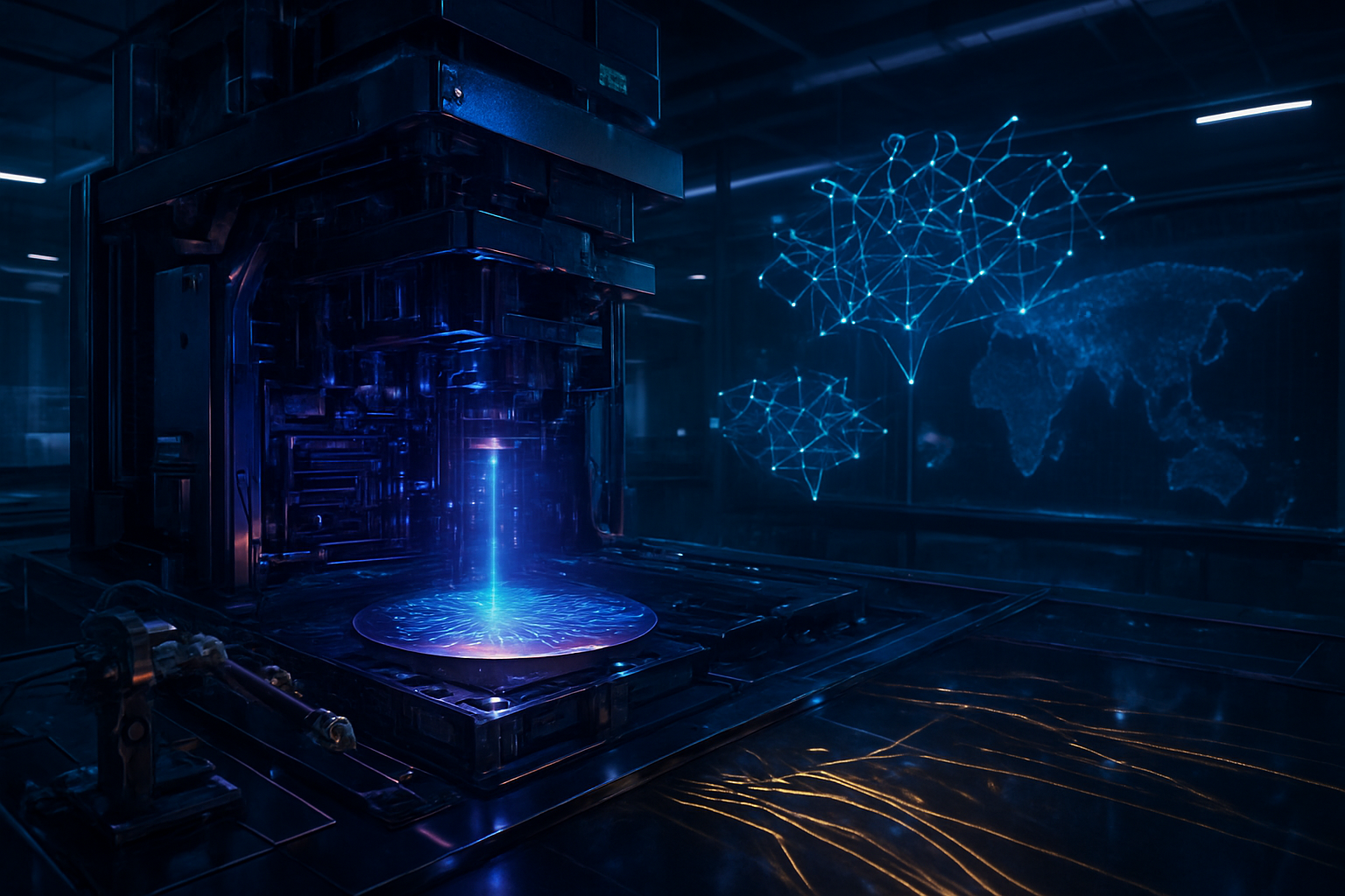
As the calendar turns to 2026, the global semiconductor landscape has been fundamentally reshaped by a seismic announcement from Shenzhen. Reports have confirmed that a high-security research facility in China’s technology hub has successfully operated a functional Extreme Ultraviolet (EUV) lithography prototype. Developed under a state-mandated "whole-of-nation" effort often referred to as the "Chinese Manhattan Project," this breakthrough marks the first time a domestic Chinese entity has solved the fundamental physics of EUV light generation—a feat previously thought to be a decade away.
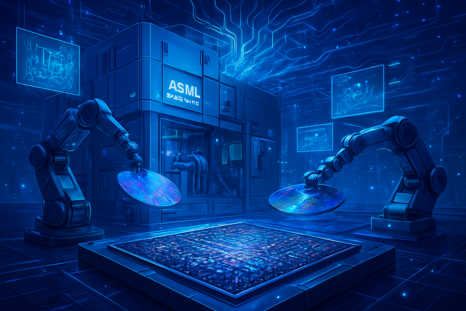
The emergence of this operational machine, which reportedly utilizes a novel Laser-Induced Discharge Plasma (LDP) light source, signals a direct challenge to the Western monopoly on leading-edge chipmaking. For years, the Dutch firm ASML Holding N.V. (NASDAQ:ASML) has been the sole provider of EUV tools, which are essential for producing chips at 7nm and below. By achieving this milestone, China has effectively punctured the "hard ceiling" of Western export controls, setting an aggressive roadmap to reach 2nm parity by 2028 and threatening to bifurcate the global technology ecosystem into two distinct, non-interoperable stacks.
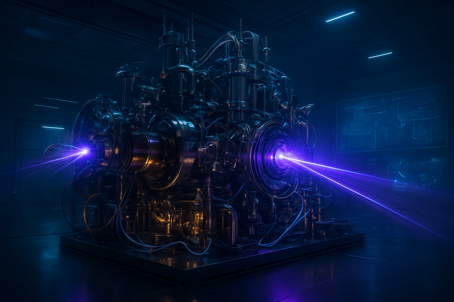
Breaking the Light Barrier: The LDP Innovation
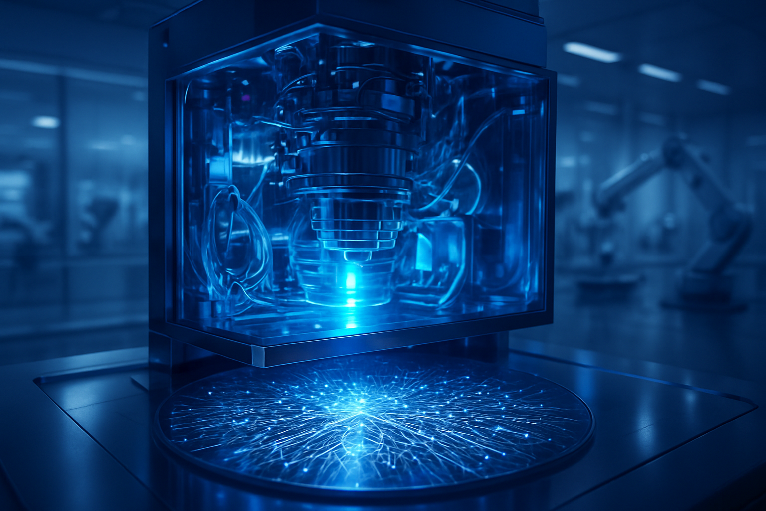
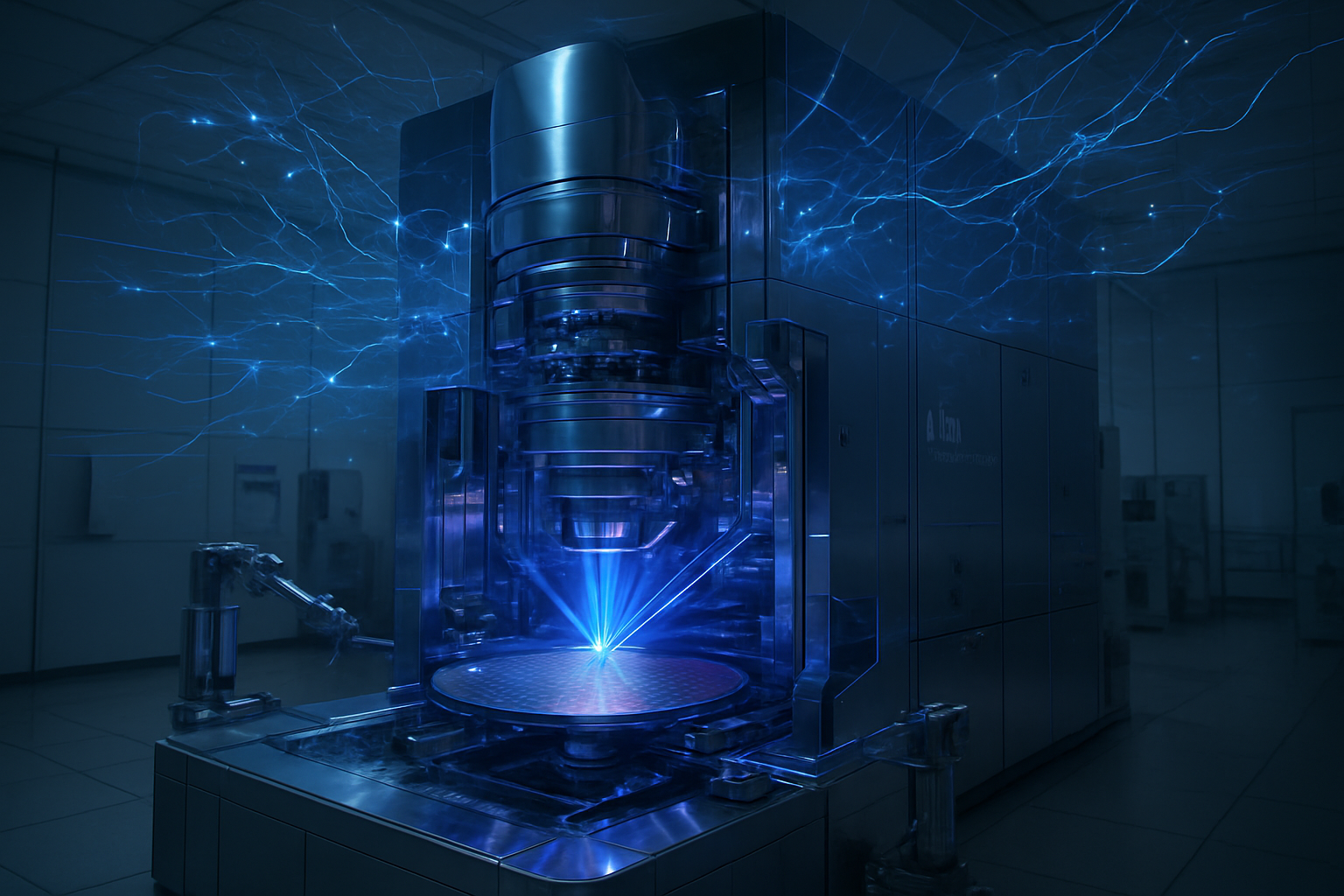
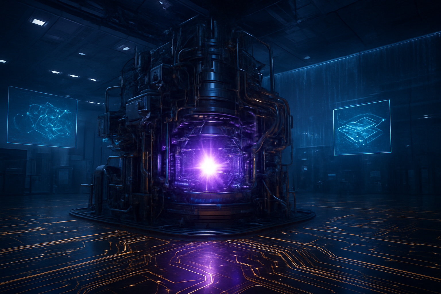
The Shenzhen prototype represents a significant departure from the industry-standard architecture pioneered by ASML. While ASML’s machines rely on Laser-Produced Plasma (LPP)—where high-power $CO_2$ lasers vaporize tin droplets 50,000 times per second—the Chinese system utilizes Laser-Induced Discharge Plasma (LDP). Developed by a consortium led by the Harbin Institute of Technology (HIT) and the Shanghai Institute of Optics and Fine Mechanics (SIOM), the LDP source uses a solid-state laser to vaporize tin, followed by a high-voltage discharge to create the plasma. This approach is technically distinct and avoids many of the specific patents held by Western firms, though it currently requires a much larger physical footprint, with the prototype reportedly filling an entire factory floor.
Technical specifications leaked from the Shenzhen facility indicate that the machine has achieved a stable 13.5nm EUV beam with a conversion efficiency of 3.42%. While this is still below the 5% to 6% efficiency required for high-volume commercial throughput, it is a massive leap from previous experimental results. The light source is currently outputting between 100W and 150W, with engineers targeting 250W for a production-ready model. The project has been bolstered by a "human intelligence" campaign that successfully recruited dozens of former ASML engineers, including high-ranking specialists like Lin Nan, who reportedly filed multiple EUV patents under an alias at SIOM after leaving the Dutch giant.
Initial reactions from the semiconductor research community have been a mix of skepticism and alarm. Experts at the Interuniversity Microelectronics Centre (IMEC) note that while the physics of the light source have been validated, the immense challenge of precision optics remains. China’s Changchun Institute of Optics, Fine Mechanics and Physics (CIOMP) is tasked with developing the objective lens assembly and interferometers required to focus that light with sub-nanometer accuracy. Industry insiders suggest that while the machine is not yet ready for mass production, it serves as a "proof of concept" that justifies the billions of dollars in state subsidies poured into the project over the last three years.
Market Shockwaves and the Rise of the 'Sovereign Stack'
The confirmation of the Shenzhen prototype has sent shockwaves through the executive suites of Silicon Valley and Hsinchu. Huawei Technologies, the primary coordinator and financier of the project, stands to be the biggest beneficiary. By integrating this domestic EUV tool into its Dongguan testing facilities, Huawei aims to secure a "sovereign supply chain" that is immune to US Department of Commerce sanctions. This development directly benefits Shenzhen-based startups like SiCarrier Technologies, which provides the critical etching and metrology tools needed to complement the EUV system, and SwaySure Technology, a Huawei-linked firm focused on domestic DRAM production.
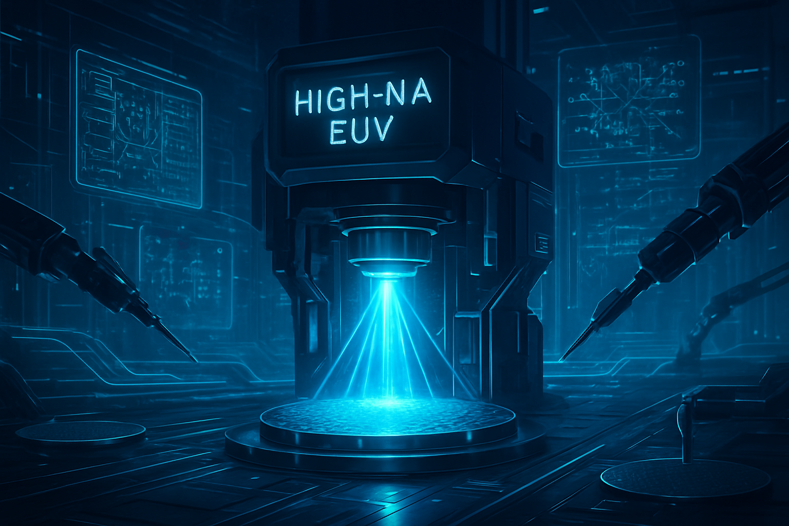
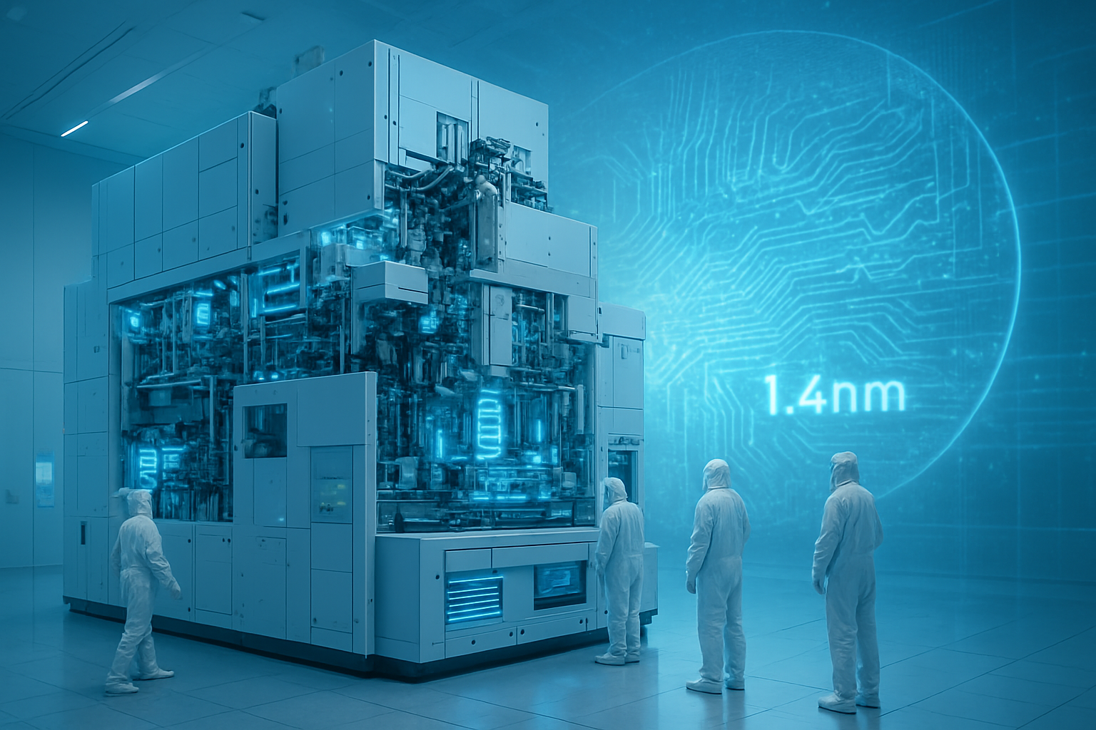
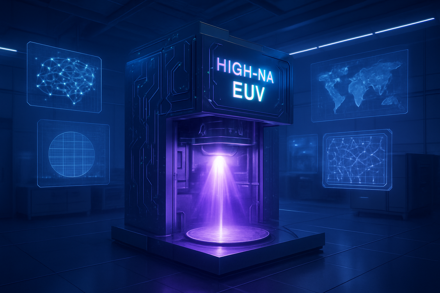
For global giants like Intel Corporation (NASDAQ:INTC) and Taiwan Semiconductor Manufacturing Company (NYSE:TSM), the breakthrough accelerates an already frantic arms race. Intel has doubled down on its "first-mover" advantage with ASML’s next-generation High-NA EUV machines, aiming to launch its 1.4nm (14A) node by late 2026 to maintain a technological "moat." Meanwhile, TSMC has reportedly accelerated its A16 and A14 roadmaps, realizing that their "Silicon Shield" now depends on maintaining a permanent two-generation lead rather than a monopoly on the equipment itself. The market positioning of ASML has also been called into question, with its stock experiencing volatility as investors price in the eventual loss of the Chinese market, which previously accounted for a significant portion of its DUV (Deep Ultraviolet) revenue.
The strategic advantage for China lies in its ability to ignore commercial margins in favor of national security. While an ASML EUV machine costs upwards of $200 million and must be profitable for a commercial fab, the Chinese "Manhattan Project" is state-funded. This allows Chinese fabs to operate at lower yields and higher costs, provided they can produce the 5nm and 3nm chips required for domestic AI accelerators like the Huawei Ascend series. This shift threatens to disrupt the existing service-based revenue models of Western toolmakers, as China moves toward a "100% domestic content" mandate for its internal chip industry.
Global Reshoring and the 'Silicon Curtain'
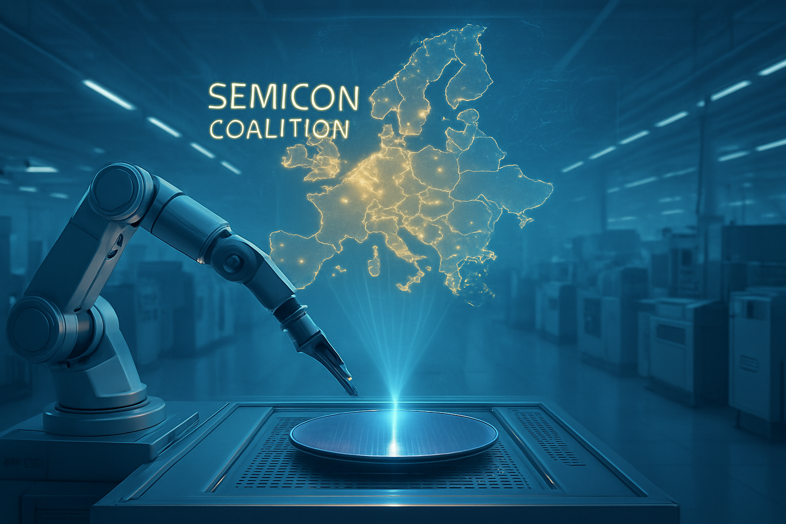
The Shenzhen breakthrough is the most significant milestone in the semiconductor industry since the invention of the transistor, signaling the end of the unified global supply chain. It fits into a broader trend of "Global Reshoring," where national governments are treating chip production as a critical utility rather than a globalized commodity. The US Department of Commerce, led by Under Secretary Howard Lutnick, has responded by moving from "selective restrictions" to "structural containment," recently revoking the "validated end-user" status for foreign-owned fabs in China to prevent the leakage of spare parts into the domestic EUV program.
This development effectively lowers a "Silicon Curtain" between the East and West. On one side is the Western "High-NA" stack, led by the US, Japan, and the Netherlands, focused on high-efficiency, market-driven, leading-edge nodes. On the other is the Chinese "Sovereign" stack, characterized by state-subsidized resilience and a "good enough" philosophy for domestic AI and military applications. The potential concern for the global economy is the creation of two non-interoperable tech ecosystems, which could lead to redundant R&D costs, incompatible AI standards, and a fragmented market for consumer electronics.
Comparisons to previous AI milestones, such as the release of GPT-4, are apt; while GPT-4 was a breakthrough in software and data, the Shenzhen EUV prototype is the hardware equivalent. It is the physical foundation upon which China’s future AI ambitions rest. Without domestic EUV, China would eventually be capped at 7nm or 5nm using multi-patterning DUV, which is prohibitively expensive and inefficient. With EUV, the path to 2nm and beyond—the "holy grail" of current semiconductor physics—is finally open to them.
The Road to 2nm: 2028 and Beyond
Looking ahead, the next 24 months will be critical for the refinement of the Shenzhen prototype. Near-term developments will likely focus on increasing the power of the LDP light source to 250W and improving the reliability of the vacuum systems. Analysts expect the first "EUV-refined" 5nm chips to roll out of Huawei’s Dongguan facility by late 2026, serving as a pilot run for more complex architectures. The ultimate goal remains 2nm parity by 2028, a target that would bring China within striking distance of the global leading edge.
However, significant challenges remain. Lithography is only one part of the puzzle; China must also master advanced packaging, photoresist chemistry, and high-purity gases—all of which are currently subject to heavy export controls. Experts predict that China will continue to use "shadow supply chains" and domestic innovation to fill these gaps. We may also see the development of alternative paths, such as Steady-State Micro-Bunching (SSMB) particle accelerators, which Beijing is exploring as a way to provide EUV light to entire clusters of lithography machines at once, potentially leapfrogging the throughput of individual ASML units.
The most immediate application for these domestic EUV chips will be in AI training and inference. As Nvidia Corporation (NASDAQ:NVDA) faces tightening restrictions on its exports to China, the pressure on Huawei to produce a 5nm or 3nm Ascend chip becomes an existential necessity for the Chinese AI industry. If the Shenzhen prototype can be successfully scaled, it will provide the compute power necessary for China to remain a top-tier player in the global AI race, regardless of Western sanctions.
A New Era of Technological Sovereignty
The successful operation of the Shenzhen EUV prototype is a watershed moment that marks the transition from a world of technological interdependence to one of technological sovereignty. The key takeaway is that the "unsolvable" problem of EUV lithography has been solved by a second global power, albeit through a different and more resource-intensive path. This development validates China’s "whole-of-nation" approach to science and technology and suggests that financial and geopolitical barriers can be overcome by concentrated state power and strategic talent acquisition.
In the context of AI history, this will likely be remembered as the moment the hardware bottleneck was broken for the world’s second-largest economy. The long-term impact will be a more competitive, albeit more divided, global tech landscape. While the West continues to lead in absolute performance through High-NA EUV and 1.4nm nodes, the "performance gap" that sanctions were intended to maintain is narrowing faster than anticipated.
In the coming weeks and months, watch for official statements from the Chinese Ministry of Industry and Information Technology (MIIT) regarding the commercialization roadmap for the "Famous Mountain" suite of tools. Simultaneously, keep a close eye on the US Department of Commerce for further "choke point" restrictions aimed at the LDP light source components. The era of the unified global chip is over; the era of the sovereign silicon stack has begun.
This content is intended for informational purposes only and represents analysis of current AI and semiconductor developments as of January 1, 2026.
TokenRing AI delivers enterprise-grade solutions for multi-agent AI workflow orchestration, AI-powered development tools, and seamless remote collaboration platforms. For more information, visit https://www.tokenring.ai/.