Tag: ASML

  • China Shatters the Silicon Monopoly: Domestic EUV Breakthrough Signals the End of ASML’s Hegemony

    China Shatters the Silicon Monopoly: Domestic EUV Breakthrough Signals the End of ASML’s Hegemony

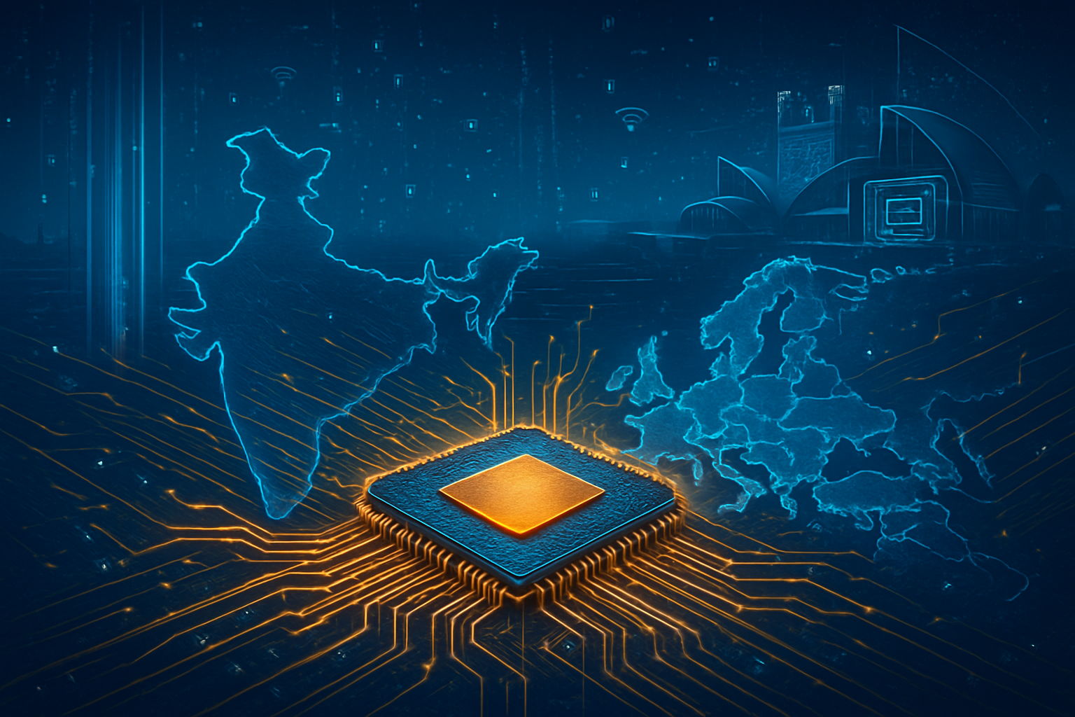
    In a development that has sent shockwaves through the global semiconductor industry, reports emerging in late 2025 confirm that China has successfully breached the "technological wall" of Extreme Ultraviolet (EUV) lithography. A high-security facility in Shenzhen has reportedly validated a functional domestic EUV prototype, marking the first time a nation has independently replicated the complex light-source technology previously monopolized by the Dutch giant ASML (NASDAQ:ASML). This breakthrough signals a decisive shift in the global "chip war," suggesting that the era of Western-led containment through equipment bottlenecks is rapidly drawing to a close.

    The immediate significance of this achievement cannot be overstated. For years, EUV lithography—the process of using 13.5nm wavelength light to etch microscopic circuits onto silicon—was considered the "Holy Grail" of manufacturing, accessible only to those with access to ASML's multi-billion dollar supply chain. China’s success in developing a working prototype, combined with Semiconductor Manufacturing International Corp (SMIC) (HKG:0981) reaching volume production on its 5nm-class nodes, effectively bypasses the most stringent U.S. export controls. This development ensures that China’s domestic AI and high-performance computing (HPC) sectors will have a sustainable, sovereign path toward the 2nm frontier.

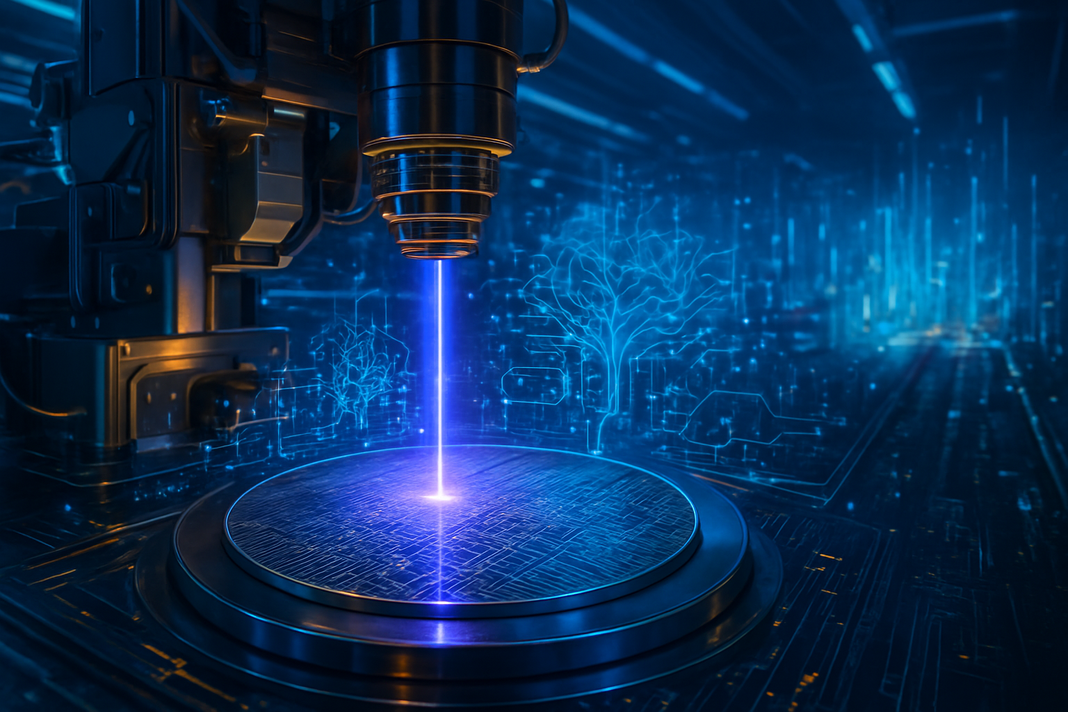
    Breaking the 13.5nm Barrier: The SSMB and LDP Revolution

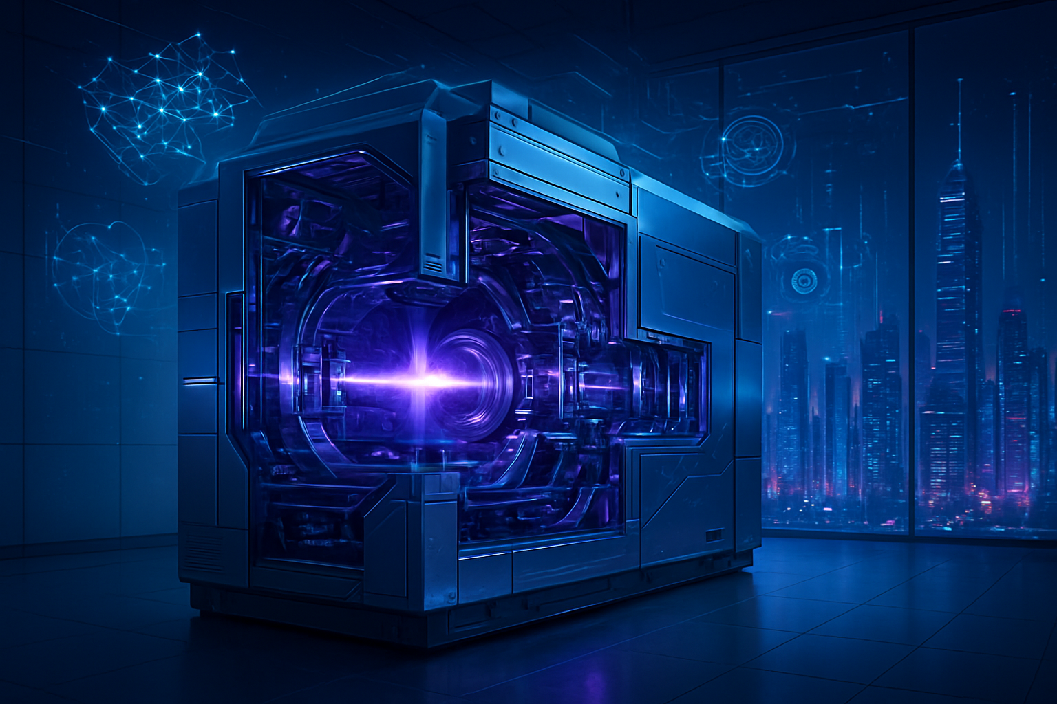
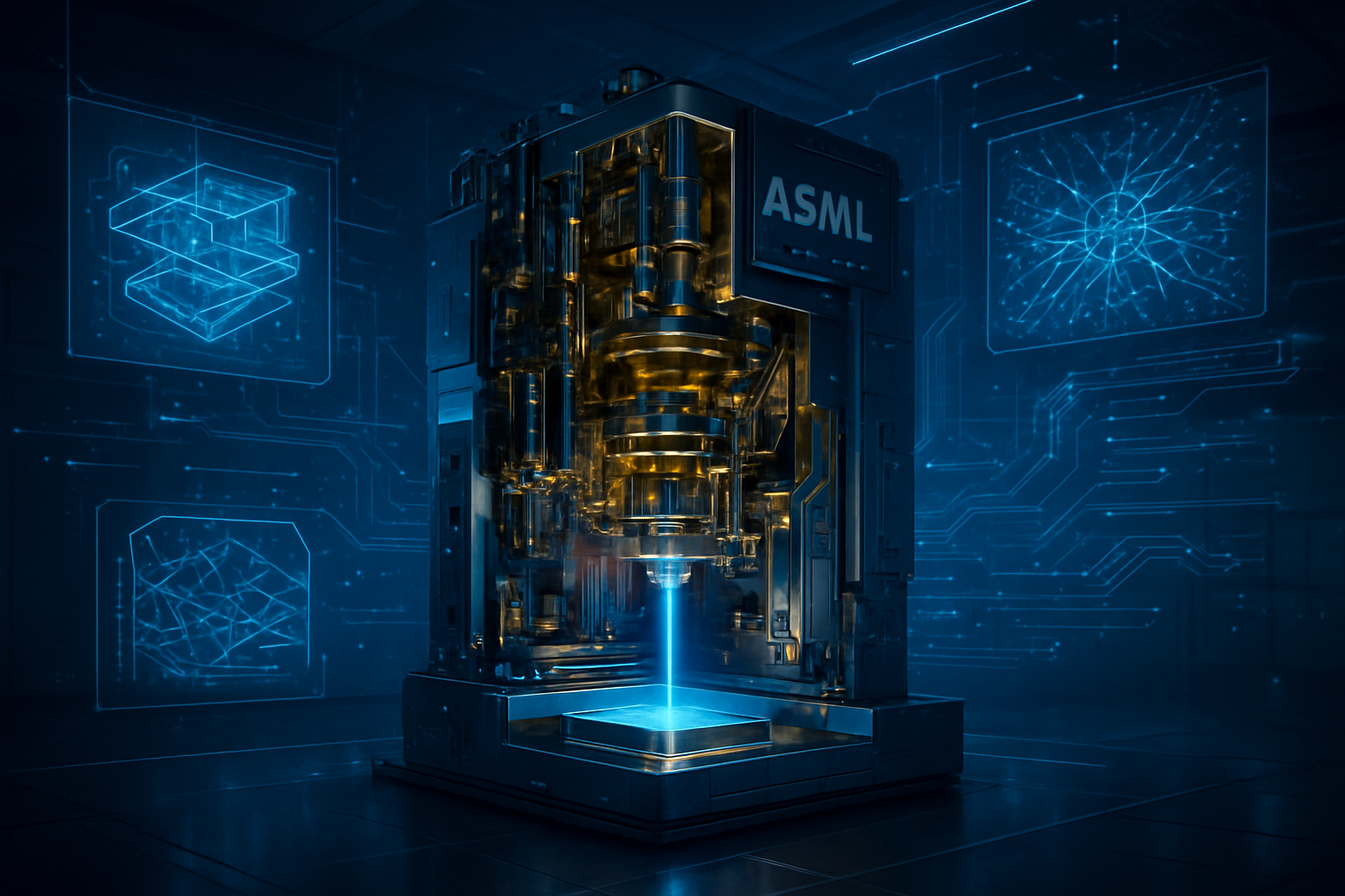
    Technically, the Chinese breakthrough deviates significantly from the architecture pioneered by ASML. While ASML utilizes Laser-Produced Plasma (LPP)—where high-power CO2 lasers vaporize tin droplets 50,000 times a second—the new Shenzhen prototype reportedly employs Laser-Induced Discharge Plasma (LDP). This method uses a combination of lasers and high-voltage discharge to generate the required plasma, a path that experts suggest is more cost-effective and simpler to maintain, even if it currently operates at a lower power output of approximately 50–100W.

    Parallel to the LDP efforts, a more radical "Manhattan Project" for chips is unfolding in Xiong'an. Led by Tsinghua University, the Steady-State Micro-Bunching (SSMB) project utilizes a particle accelerator to generate a "clean" and continuous EUV beam. Unlike the pulsed light of traditional lithography, SSMB could theoretically reach power levels of 1kW or higher, potentially leapfrogging ASML’s current High-NA EUV capabilities by providing a more stable light source with fewer debris issues. This dual-track approach—LDP for immediate industrial application and SSMB for future-generation dominance—demonstrates a sophisticated R&D strategy that has outpaced Western intelligence estimates.

    Furthermore, Huawei has played a pivotal role as the coordinator of a "shadow supply chain." Recent patent filings reveal that Huawei and its partner SiCarrier have perfected Self-Aligned Quadruple Patterning (SAQP) for 2nm-class features. While this "brute force" method using older Deep Ultraviolet (DUV) tools was once considered economically unviable due to low yields, the integration of domestic EUV prototypes is expected to stabilize production. Initial reactions from the international research community suggest that while China still trails in yield efficiency, the fundamental physics and engineering hurdles have been cleared.

    Market Disruption: ASML’s Demand Cliff and the Rise of the "Two-Track" Supply Chain

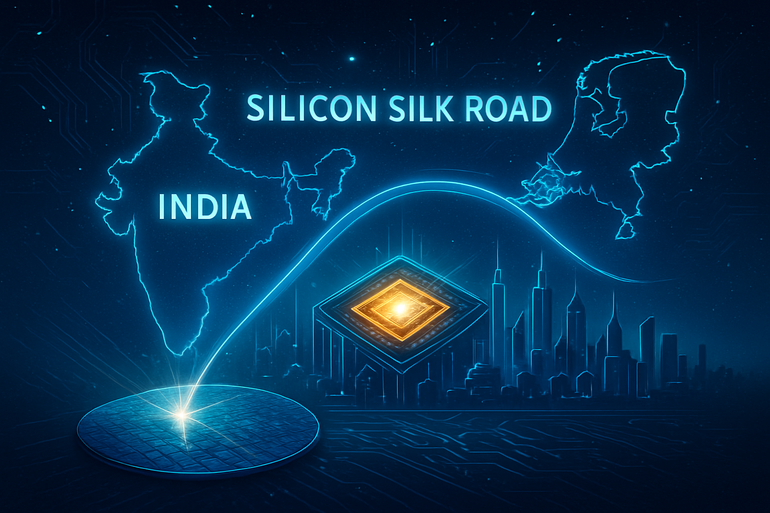
    The emergence of a viable Chinese EUV alternative poses an existential threat to the current market structure. ASML (NASDAQ:ASML), which has long enjoyed a 100% market share in EUV equipment, now faces what analysts call a "long-term demand cliff" in China—previously its most profitable region. While ASML’s 2025 revenues remained buoyed by Chinese firms stockpiling DUV spare parts, the projection for 2026 and beyond shows a sharp decline as domestic alternatives from Shanghai Micro Electronics Equipment (SMEE) and SiCarrier begin to replace Dutch and Japanese components in metrology and wafer handling.

    The competitive implications extend to the world’s leading foundries. Taiwan Semiconductor Manufacturing Company (TSMC) (NYSE:TSM) and Intel (NASDAQ:INTC) are now facing a competitor in SMIC that is no longer bound by international sanctions. Although SMIC’s 5nm yields are currently estimated at 33% to 35%—far below TSMC’s ~85%—the massive $47.5 billion "Big Fund" Phase III provides the financial cushion necessary to absorb these costs. For Chinese AI giants like Baidu (NASDAQ:BIDU) and Alibaba (NYSE:BABA), this means a guaranteed supply of domestic chips for their large language models, reducing their reliance on "stripped-down" export-compliant chips from Nvidia (NASDAQ:NVDA).

    Moreover, the strategic advantage is shifting toward "good enough" sovereign technology. Even if Chinese EUV machines are 50% more expensive to operate per wafer, the removal of geopolitical risk is a premium the Chinese government is willing to pay. This is forcing global tech giants to reconsider their manufacturing footprints, as the "Two-Track World"—one supply chain for the West and an entirely separate, vertically integrated one for China—becomes a permanent reality.

    Geopolitical Fallout: The Export Control Paradox

    The success of China’s EUV program highlights the "Export Control Paradox": the very sanctions intended to stall China’s progress served as the ultimate accelerant. By cutting off access to ASML and Lam Research (NASDAQ:LRCX) equipment, the U.S. and its allies forced Chinese firms to collaborate with domestic academia and the military-industrial complex in ways that were previously fragmented. The result is a semiconductor landscape that is more resilient and less dependent on global trade than it was in 2022.

    This development fits into a broader trend of "technological sovereignty" that is defining the mid-2020s. Similar to how the launch of Sputnik galvanized the U.S. space program, the "EUV breakthrough" is being hailed in Beijing as a landmark victory for the socialist market economy. However, it also raises significant concerns regarding global security. A China that is self-sufficient in advanced silicon is a China that is less vulnerable to economic pressure, potentially altering the calculus for regional stability in the Taiwan Strait and the South China Sea.

    Comparisons are already being made to the 1960s nuclear breakthroughs. Just as the world had to adjust to a multi-polar nuclear reality, the semiconductor industry must now adjust to a multi-polar advanced manufacturing reality. The era where a single company in Veldhoven, Netherlands, could act as the gatekeeper for the world’s most advanced AI applications has effectively ended.

    The Road to 2nm: What Lies Ahead

    Looking toward 2026 and 2027, the focus will shift from laboratory prototypes to industrial scaling. The primary challenge for China remains yield optimization. While producing a functional 5nm chip is a feat, producing millions of them at a cost that competes with TSMC is another matter entirely. Experts predict that China will focus on "advanced packaging" and "chiplet" designs to compensate for lower yields, effectively stitching together smaller, functional dies to create massive AI accelerators.

    The next major milestone to watch will be the completion of the SSMB-EUV light source facility in Xiong'an. If this particle accelerator-based approach becomes operational for mass production, it could theoretically allow China to produce 2nm and 1nm chips with higher efficiency than ASML’s current High-NA systems. This would represent a complete leapfrog event, moving China from a follower to a leader in lithography physics.

    However, significant challenges remain. The ultra-precision optics required for EUV—traditionally provided by Carl Zeiss for ASML—are notoriously difficult to manufacture. While the Changchun Institute of Optics has made strides, the durability and coating consistency of domestic mirrors under intense EUV radiation will be the ultimate test of the system's longevity in a 24/7 factory environment.

    Conclusion: A New Era of Global Competition

    The reports of China’s EUV breakthrough mark a definitive turning point in the history of technology. It proves that with sufficient capital, state-level coordination, and a clear strategic mandate, even the most complex industrial monopolies can be challenged. The key takeaways are clear: China has successfully transitioned from "brute-forcing" 7nm chips to developing the fundamental tools for sub-5nm manufacturing, and the global semiconductor supply chain has irrevocably split into two distinct spheres.

    In the history of AI and computing, this moment will likely be remembered as the end of the "unipolar silicon era." The long-term impact will be a more competitive, albeit more fragmented, global market. For the tech industry, the coming months will be defined by a scramble to adapt to this new reality. Investors and policymakers should watch for the first "all-domestic" 5nm chip releases from Huawei in early 2026, which will serve as the ultimate proof of concept for this new era of Chinese semiconductor sovereignty.


    This content is intended for informational purposes only and represents analysis of current AI and semiconductor developments.

    TokenRing AI delivers enterprise-grade solutions for multi-agent AI workflow orchestration, AI-powered development tools, and seamless remote collaboration platforms.
    For more information, visit https://www.tokenring.ai/.

  • Silicon Silk Road: India and EU Forge Historic Semiconductor Alliance with the Netherlands as the Strategic Pivot

    Silicon Silk Road: India and EU Forge Historic Semiconductor Alliance with the Netherlands as the Strategic Pivot

    As of December 19, 2025, the geopolitical map of the global technology sector is being redrawn. India and the European Union have entered the final, decisive phase of their landmark Free Trade Agreement (FTA) negotiations, with a formal signing now scheduled for January 27, 2026. At the heart of this historic deal is a sophisticated framework for semiconductor cooperation that aims to bridge the technological chasm between the two regions. This "Silicon Silk Road" initiative represents a strategic pivot, positioning India as a primary manufacturing and design hub for European tech interests while securing the EU’s supply chain against future global shocks.

    The immediate significance of this development cannot be overstated. By synchronizing the €43 billion EU Chips Act with the $10 billion India Semiconductor Mission (ISM), both regions are moving beyond mere trade to deep industrial integration. Today’s finalization of a series of bilateral Memorandums of Understanding (MoUs) between India and the Netherlands marks the operational start of this alliance. These agreements focus on high-stakes technology transfer, advanced lithography maintenance, and the creation of a "verified hardware" corridor that will define the next decade of AI and automotive electronics.

    Technical Synergy and the GANANA Project

    The technical backbone of this cooperation is managed through the India-EU Trade and Technology Council (TTC), which has moved from policy discussion to hardware implementation. A standout development is the GANANA Project, a €5 million initiative funded via Horizon Europe. This project establishes a high-performance computing (HPC) corridor linking Europe’s pre-exascale supercomputers, such as LUMI in Finland and Leonardo in Italy, with India’s Centre for Development of Advanced Computing (C-DAC). This link allows Indian engineers to perform AI-driven semiconductor modeling and "digital twin" simulations of fabrication processes before a single wafer is etched in India’s new fabs in Gujarat and Assam.

    Furthermore, the cooperation is targeting the "missing middle" of the semiconductor value chain: advanced chip design and Process Design Kits (PDKs). Unlike previous technology transfers that focused on lagging-edge nodes, the current framework emphasizes heterogeneous integration and compound semiconductors. This involves the use of Gallium Nitride (GaN) and Silicon Carbide (SiC), materials essential for the next generation of electric vehicles (EVs) and 6G infrastructure. By sharing PDKs—the specialized software tools used to design chips for specific foundry processes—the EU is effectively providing Indian startups with the "blueprints" needed to compete at a global level.

    Industry experts have reacted with cautious optimism, noting that this differs from existing technology partnerships by focusing on "sovereign hardware." The goal is to create a supply chain that is not only efficient but also "secure-by-design," ensuring that the chips powering critical infrastructure in both regions are free from backdoors or vulnerabilities. This level of technical transparency is unprecedented between a Western bloc and a major emerging economy.

    Corporate Giants and the Dutch Bridge

    The Netherlands has emerged as the indispensable bridge in this partnership, leveraging its status as a global leader in precision engineering and lithography. ASML Holding N.V. (NASDAQ: ASML) has shifted its Indian strategy from a vendor model to an infrastructure-support model. Rather than simply exporting Deep Ultraviolet (DUV) lithography machines, ASML is establishing specialized maintenance and training labs within India. These hubs are designed to train a new generation of Indian lithography engineers, ensuring that the multi-billion dollar fabrication units being built by the Tata Group and other domestic players operate with the yields required for commercial viability.

    Meanwhile, NXP Semiconductors N.V. (NASDAQ: NXPI) is deepening its footprint with a $1 billion expansion plan that includes a massive new R&D hub in the Greater Noida Semiconductor Park. This facility is tasked with leading NXP’s global efforts in 5nm automotive AI chips. By doubling its Indian engineering workforce to 6,000 by 2028, NXP is effectively making India the nerve center for its global automotive and IoT (Internet of Things) chip design. This move provides NXP with a strategic advantage, tapping into India's vast pool of VLSI (Very Large Scale Integration) designers while providing India with direct access to cutting-edge automotive tech.

    Other major players are also positioning themselves to benefit. The HCL-Foxconn joint venture for an Outsourced Semiconductor Assembly and Test (OSAT) plant in Uttar Pradesh is reportedly integrating Dutch metrology and inspection software. This integration ensures that Indian-packaged chips meet the stringent quality standards required for the European automotive and aerospace markets, facilitating a seamless flow of components across the "Silicon Silk Road."

    Geopolitical De-risking and AI Sovereignty

    The wider significance of the India-EU semiconductor nexus lies in the global trend of "de-risking" and "friend-shoring." As the world moves away from a China-centric supply chain, the India-EU alliance offers a robust alternative. For the EU, India provides the scale and human capital that Europe lacks; for India, the EU provides the high-end IP and precision machinery that are difficult to develop from scratch. This partnership is a cornerstone of the broader "AI hardware sovereignty" movement, where nations seek to ensure they have the physical capacity to run the AI models of the future.

    However, the path is not without its challenges. The EU’s Carbon Border Adjustment Mechanism (CBAM) remains a point of contention in the broader FTA negotiations. India is concerned that the "green" tariffs on steel and cement could offset the economic gains from tech cooperation. Conversely, European labor unions have expressed concerns about the "Semiconductor Skills Program," which facilitates the mobility of Indian engineers into Europe, fearing it could lead to wage stagnation in the local tech sector.

    Despite these hurdles, the comparison to previous milestones is clear. This is not just a trade deal; it is a "tech-industrial pact" similar in spirit to the post-WWII alliances that built the modern aerospace industry. By aligning the EU Chips Act 2.0 with India’s ISM 2.0, the two regions are attempting to create a bipolar tech ecosystem that can balance the dominance of the United States and East Asia.

    The Horizon: 2D Materials and 6G

    Looking ahead, the next phase of this cooperation will likely move into the realm of "Beyond CMOS" technologies. Research institutions like IMEC in Belgium are already discussing joint pilot lines with Indian universities for 2D materials and carbon nanotubes. These materials could eventually replace silicon, offering a path to even faster and more energy-efficient AI processors. In the near term, expect to see the first "Made in India" chips using Dutch lithography hitting the European market by late 2026, primarily in the automotive and industrial sectors.

    Applications for this cooperation will soon extend to 6G telecommunications. The India-EU TTC has already identified 6G as a priority area, with plans to develop joint standards that prioritize privacy and decentralized architecture. The challenge will be maintaining the momentum of these capital-intensive projects through potential economic cycles. Experts predict that the success of the January 2026 signing will trigger a wave of venture capital investment into Indian "fabless" chip startups, which can now design for a guaranteed European market.

    Conclusion: A New Era of Tech Diplomacy

    The finalization of the India-Netherlands semiconductor MoUs on December 19, 2025, marks a watershed moment in technology diplomacy. It signals that the "tech gap" is no longer a barrier but a bridge, with the Netherlands acting as the vital link between European innovation and Indian industrial scale. The impending signing of the India-EU FTA in January 2026 will codify this relationship, creating a powerful new bloc in the global semiconductor landscape.

    The long-term impact of this development will be felt in the democratization of high-end chip manufacturing and the acceleration of AI deployment across the Global South and Europe. As we move into 2026, the industry will be watching the progress of the first joint pilot lines and the mobility of talent between Eindhoven and Bengaluru. The "Silicon Silk Road" is no longer a vision—it is an operational reality that promises to redefine the global digital economy for decades to come.


    This content is intended for informational purposes only and represents analysis of current AI developments.

    TokenRing AI delivers enterprise-grade solutions for multi-agent AI workflow orchestration, AI-powered development tools, and seamless remote collaboration platforms.
    For more information, visit https://www.tokenring.ai/.

  • The Silent Architects of Intelligence: Why Semiconductor Manufacturing Stocks Defined the AI Era in 2025

    The Silent Architects of Intelligence: Why Semiconductor Manufacturing Stocks Defined the AI Era in 2025

    As 2025 draws to a close, the narrative surrounding artificial intelligence has undergone a fundamental shift. While the previous two years were defined by the meteoric rise of generative AI software and the viral success of large language models, 2025 has been the year of the "Mega-Fab." The industry has moved beyond debating the capabilities of chatbots to the grueling, high-stakes reality of physical production. In this landscape, the "picks and shovels" of the AI revolution—the semiconductor manufacturing and equipment companies—have emerged as the true power brokers of the global economy.

    The significance of these manufacturing giants cannot be overstated. As of December 19, 2025, global semiconductor sales have hit a record-breaking $697 billion, driven almost entirely by the insatiable demand for AI-grade silicon. While chip designers capture the headlines, it is the companies capable of manipulating matter at the atomic scale that have dictated the pace of AI progress this year. From the rollout of 2nm process nodes to the deployment of High-NA EUV lithography, the physical constraints of manufacturing are now the primary frontier of artificial intelligence.

    Atomic Precision: The Technical Triumph of 2nm and High-NA EUV

    The technical milestone of 2025 has undoubtedly been the successful volume production of the 2nm (N2) process node by Taiwan Semiconductor Manufacturing Company (NYSE: TSM). After years of development, TSMC confirmed this quarter that yield rates at its Baoshan and Kaohsiung facilities have exceeded 70%, a feat many analysts thought impossible by this date. This new node utilizes Gate-All-Around (GAA) transistor architecture, which provides a significant leap in energy efficiency and performance over the previous FinFET designs. For AI, this translates to chips that can process more parameters per watt, a critical metric as data center power consumption reaches critical levels.

    Supporting this transition is the mass deployment of High-NA (Numerical Aperture) Extreme Ultraviolet (EUV) lithography systems. ASML (NASDAQ: ASML) solidified its monopoly on this front in 2025, completing shipments of the Twinscan EXE:5200B to key partners. These machines, costing over $350 million each, allow for a higher resolution in chip printing, enabling the industry to push toward the 1.4nm (14A) threshold. Unlike previous lithography generations, High-NA EUV eliminates the need for complex multi-patterning, streamlining the manufacturing process for the ultra-dense processors required for next-generation AI training.

    Furthermore, the role of materials engineering has taken center stage. Applied Materials (NASDAQ: AMAT) has maintained a dominant 18% market share in wafer fabrication equipment by pioneering new techniques in Backside Power Delivery (BPD). By moving power wiring to the underside of the silicon wafer, companies like Applied Materials have solved the "routing congestion" that plagued earlier AI chip designs. This technical shift, combined with advanced "Chip on Wafer on Substrate" (CoWoS) packaging, has allowed manufacturers to stack logic and memory with unprecedented density, effectively breaking the memory wall that previously throttled AI performance.

    The Infrastructure Moat: Market Impact and Strategic Advantages

    The market performance of these manufacturing stocks in 2025 reflects their role as the backbone of the industry. While Nvidia (NASDAQ: NVDA) remains a central figure, its growth has stabilized as the market recognizes that its success is entirely dependent on the production capacity of its partners. In contrast, equipment and memory providers have seen explosive growth. Micron Technology (NASDAQ: MU), for instance, has surged 141% year-to-date, fueled by its dominance in HBM3e (High-Bandwidth Memory), which is essential for feeding data to AI GPUs at light speed.

    This shift has created a formidable "infrastructure moat" for established players. The sheer capital intensity required to compete at the 2nm level—estimated at over $25 billion per fab—has effectively locked out new entrants and even put pressure on traditional giants. While Intel (NASDAQ: INTC) has made significant strides in reaching parity with its 18A process in Arizona, the competitive advantage remains with those who control the equipment supply chain. Companies like Lam Research (NASDAQ: LRCX), which specializes in the etching and deposition processes required for 3D chip stacking, have seen their order backlogs swell to record highs as every major foundry races to expand capacity.

    The strategic advantage has also extended to the "plumbing" of the AI era. Vertiv Holdings (NYSE: VRT) has become a surprise winner of 2025, providing the liquid cooling systems necessary for the high-heat environments of AI data centers. As the industry moves toward massive GPU clusters, the ability to manage power and heat has become as valuable as the chips themselves. This has led to a broader market realization: the AI revolution is not just a software race, but a massive industrial mobilization that favors companies with deep expertise in physical engineering and logistics.

    Geopolitics and the Global Silicon Landscape

    The wider significance of these developments is deeply intertwined with global geopolitics and the "reshoring" of technology. Throughout 2025, the implementation of the CHIPS Act in the United States and similar initiatives in Europe have begun to bear fruit, with new leading-edge facilities coming online in Arizona, Ohio, and Germany. However, this transition has not been without friction. U.S. export restrictions have forced companies like Applied Materials and Lam Research to pivot away from the Chinese market, which previously accounted for a significant portion of their revenue.

    Despite these challenges, the broader AI landscape has benefited from a more diversified supply chain. The move toward domestic manufacturing has mitigated some of the risks associated with regional instability, though TSMC’s dominance in Taiwan remains a focal point of global economic security. The "Picks and Shovels" companies have acted as a stabilizing force, providing the standardized tools and materials that allow for a degree of interoperability across different foundries and regions.

    Comparing this to previous milestones, such as the mobile internet boom or the rise of cloud computing, the AI era is distinct in its demand for sheer physical scale. We are no longer just shrinking transistors; we are re-engineering the very way data moves through matter. This has raised concerns regarding the environmental impact of such a massive industrial expansion. The energy required to run these "Mega-Fabs" and the data centers they supply has forced a renewed focus on sustainability, leading to innovations in low-power silicon and more efficient manufacturing processes that were once considered secondary priorities.

    The Horizon: Silicon Photonics and the 1nm Roadmap

    Looking ahead to 2026 and beyond, the industry is already preparing for the next major leap: silicon photonics. This technology, which uses light instead of electricity to transmit data between chips, is expected to solve the interconnect bottlenecks that currently limit the size of AI clusters. Experts predict that companies like Lumentum (NASDAQ: LITE) and Fabrinet (NYSE: FN) will become the next tier of essential manufacturing stocks as optical interconnects move from niche applications to the heart of the AI data center.

    The roadmap toward 1nm and "sub-angstrom" manufacturing is also becoming clearer. While the technical challenges of quantum tunneling and heat dissipation become more acute at these scales, the collaboration between ASML, TSMC, and Applied Materials suggests that the "Moore’s Law is Dead" narrative may once again be premature. The next two years will likely see the first pilot lines for 1.4nm production, utilizing even more advanced High-NA EUV techniques and new 2D materials like molybdenum disulfide to replace traditional silicon channels.

    However, challenges remain. The talent shortage in semiconductor engineering continues to be a bottleneck, and the inflationary pressure on raw materials like neon and rare earth elements poses a constant threat to margins. As we move into 2026, the focus will likely shift toward "software-defined manufacturing," where AI itself is used to optimize the yields and efficiency of the fabs that create it, creating a virtuous cycle of silicon-driven intelligence.

    A New Era of Industrial Intelligence

    The story of AI in 2025 is the story of the factory floor. The companies profiled here—TSMC, Applied Materials, ASML, and their peers—have proven that the digital future is built on a physical foundation. Their ability to deliver unprecedented precision at a global scale has enabled the current AI boom and will dictate the limits of what is possible in the years to come. The "picks and shovels" are no longer just supporting actors; they are the lead protagonists in the most significant technological shift of the 21st century.

    As we look toward the coming weeks, investors and industry watchers should keep a close eye on the Q4 earnings reports of the major equipment manufacturers. These reports will serve as a bellwether for the 2026 capital expenditure plans of the world’s largest tech companies. If the current trend holds, the "Mega-Fab" era is only just beginning, and the silent architects of intelligence will continue to be the most critical stocks in the global market.


    This content is intended for informational purposes only and represents analysis of current AI developments.

    TokenRing AI delivers enterprise-grade solutions for multi-agent AI workflow orchestration, AI-powered development tools, and seamless remote collaboration platforms.
    For more information, visit https://www.tokenring.ai/.

  • The Silicon Silk Road: India and the Netherlands Forge a New Semiconductor Axis for the AI Era

    The Silicon Silk Road: India and the Netherlands Forge a New Semiconductor Axis for the AI Era

    In a move that signals a tectonic shift in the global technology landscape, India and the Netherlands have today, December 19, 2025, finalized the "Silicon Silk Road" strategic alliance. This comprehensive framework, signed in New Delhi, aims to bridge the gap between European high-tech precision and Indian industrial scale. By integrating the Netherlands’ world-leading expertise in lithography and semiconductor equipment with India’s rapidly expanding manufacturing ecosystem, the partnership seeks to create a resilient, alternative supply chain for the high-performance hardware required to power the next generation of artificial intelligence.

    The immediate significance of this alliance cannot be overstated. As the global demand for AI-optimized chips—specifically those capable of handling massive large language model (LLM) training and edge computing—reaches a fever pitch, the "Silicon Silk Road" provides a blueprint for a decentralized manufacturing future. The agreement moves beyond simple trade, establishing a co-development model that includes technology transfers, joint R&D in advanced materials, and the creation of specialized maintenance hubs that will ensure India’s upcoming fabrication units (fabs) operate with the world’s most advanced Dutch-made machinery.

    Technical Foundations: Lithography, Labs, and Lab-Grown Diamonds

    The core of the alliance is built upon unprecedented commitments from Dutch semiconductor giants. NXP Semiconductors N.V. (NASDAQ:NXPI) has officially announced a massive $1 billion investment to double its research and development presence in India. This expansion is focused on the design of 5-nanometer automotive and AI chips, with a new R&D center slated for the Greater Noida Semiconductor Park. Unlike previous design-only centers, this facility will work in tandem with Indian manufacturing partners to prototype "system-on-chip" (SoC) architectures specifically optimized for low-latency AI applications.

    Simultaneously, ASML Holding N.V. (NASDAQ:ASML) is shifting its strategy from a vendor-client relationship to a deep-tier partnership. For the first time, ASML will establish "Holistic Lithography" maintenance labs within India. These labs are designed to provide real-time technical support and software calibration for the Extreme Ultraviolet (EUV) and Deep Ultraviolet (DUV) lithography systems that are essential for high-end chip production. This differs from existing models where technical expertise was centralized in Europe or East Asia, effectively removing a significant bottleneck for Indian fab operators like the Tata Group and Micron Technology, Inc. (NASDAQ:MU).

    One of the most technically ambitious aspects of the 2025 framework is the joint research into lab-grown diamonds (LGD) as a substrate for semiconductors. Leveraging India’s established diamond-processing hub in Surat and Dutch precision engineering, the partnership aims to develop diamond-based chips that can handle significantly higher thermal loads than traditional silicon. This breakthrough could revolutionize AI hardware, where heat management is currently a primary limiting factor for processing density in data centers.

    Strategic Realignment: Winners in the New Hardware Race

    The "Silicon Silk Road" creates a new competitive theater for the world’s largest AI labs and hardware providers. Companies like NVIDIA Corporation (NASDAQ:NVDA) and Advanced Micro Devices, Inc. (NASDAQ:AMD) stand to benefit immensely from a more diversified manufacturing base. By having a viable, Dutch-supported manufacturing alternative in India, these tech giants can mitigate the geopolitical risks associated with the current concentration of production in East Asia. The alliance provides a "China+1" strategy with teeth, offering a stable environment backed by European intellectual property protections and Indian production-linked incentives (PLI).

    For the Netherlands, the alliance secures a massive, long-term market for its high-tech exports at a time when global trade restrictions are tightening. ASML and NXP are effectively "future-proofing" their revenue streams by embedding themselves into the foundation of India’s digital infrastructure. Meanwhile, Indian tech conglomerates and startups are gaining access to the "holy grail" of semiconductor manufacturing: the ability to move from chip design to domestic fabrication with the support of the world’s most advanced equipment manufacturers. This positioning gives Indian firms a strategic advantage in the burgeoning field of "Sovereign AI," where nations seek to control their own computational resources.

    Geopolitics and the Global AI Landscape

    The emergence of the Silicon Silk Road fits into a broader trend of "techno-nationalism," where semiconductor self-sufficiency is viewed as a pillar of national security. This partnership is a direct response to the fragility of global supply chains exposed during the early 2020s. By forging this link, India and the Netherlands are creating a middle path that avoids the binary choice between US-led and China-led ecosystems. It is a milestone comparable to the early 2000s outsourcing boom, but with a critical difference: this time, India is moving up the value chain into the most complex manufacturing process ever devised by humanity.

    However, the alliance does not come without concerns. Industry analysts have pointed to the immense energy requirements of advanced fabs and the potential environmental impact of large-scale semiconductor manufacturing in India. Furthermore, the transfer of highly sensitive lithography technology requires a level of cybersecurity and intellectual property protection that will be a constant test for Indian regulators. Comparing this to previous milestones like the CHIPS Act, the Silicon Silk Road is unique because it relies on bilateral synergy rather than unilateral subsidies, blending Dutch technical precision with India’s demographic dividend.

    The Horizon: 2026 and Beyond

    Looking ahead, the next 24 months will be critical for the execution of the 2025 framework. The immediate goal is the operationalization of the first joint R&D labs and the commencement of training for the first cohort of 85,000 semiconductor professionals that India aims to produce by 2030. Near-term developments will likely include the announcement of a joint venture between an Indian industrial house and a Dutch equipment firm to manufacture semiconductor components—not just chips—locally, further deepening the supply chain.

    The long-term vision involves the commercialization of the lab-grown diamond substrate technology, which could place the India-Netherlands axis at the forefront of "Beyond Silicon" computing. Experts predict that by 2028, the first AI accelerators featuring "Made in India" chips, fabricated using ASML-supported systems, will hit the global market. The primary challenge will be maintaining the pace of infrastructure development—specifically stable power and ultra-pure water supplies—to match the requirements of the high-tech machinery being deployed.

    Conclusion: A New Chapter in Industrial History

    The signing of the Silicon Silk Road alliance marks the end of an era where semiconductor manufacturing was the exclusive domain of a few select geographies. It represents a maturation of India’s industrial ambitions and a strategic pivot for the Netherlands as it seeks to maintain its technological edge in an increasingly fragmented world. The key takeaway is clear: the future of AI hardware will not be determined by a single nation, but by the strength and resilience of the networks they build.

    As we move into 2026, the global tech community will be watching the progress in Greater Noida and the research labs of Eindhoven with intense interest. The success of this partnership could serve as a model for other nations looking to secure their technological future. For now, the "Silicon Silk Road" stands as a testament to the power of strategic collaboration in the age of artificial intelligence, promising to reshape the hardware that will define the rest of the 21st century.


    This content is intended for informational purposes only and represents analysis of current AI developments.

    TokenRing AI delivers enterprise-grade solutions for multi-agent AI workflow orchestration, AI-powered development tools, and seamless remote collaboration platforms.
    For more information, visit https://www.tokenring.ai/.

  • The Silicon Shield: India and the Netherlands Forge Strategic Alliance in Secure Semiconductor Hardware

    The Silicon Shield: India and the Netherlands Forge Strategic Alliance in Secure Semiconductor Hardware

    NEW DELHI — In a landmark move that signals a paradigm shift in the global technology landscape, India and the Netherlands have finalized a series of strategic agreements aimed at securing the physical foundations of artificial intelligence. On December 19, 2025, during a high-level diplomatic summit in New Delhi, officials from both nations concluded six comprehensive Memoranda of Understanding (MoUs) that bridge Dutch excellence in semiconductor lithography with India’s massive "IndiaAI" mission and manufacturing ambitions. This partnership, described by diplomats as the "Indo-Dutch Strategic Technology Alliance," prioritizes "secure-by-design" hardware—a critical move to ensure that the next generation of AI infrastructure is inherently resistant to cyber-tampering and state-sponsored espionage.

    The immediate significance of this alliance cannot be overstated. As AI models become increasingly integrated into critical infrastructure—from autonomous power grids to national defense systems—the vulnerability of the underlying silicon has become a primary national security concern. By moving beyond a simple buyer-seller relationship, India and the Netherlands are co-developing a "Silicon Shield" that integrates security protocols directly into the chip architecture. This initiative is a cornerstone of India’s $20 billion India Semiconductor Mission (ISM) 2.0, positioning the two nations as a formidable alternative to the traditional technology duopoly of the United States and China.

    Technical Deep Dive: Secure-by-Design and Hardware Root of Trust

    The technical core of this partnership centers on the "Secure-by-Design" philosophy, which mandates that security features be integrated at the architectural level of a chip rather than as a software patch after fabrication. A key component of this initiative is the development of Hardware Root of Trust (HRoT) systems. Unlike previous security measures that relied on volatile software environments, HRoT provides a permanent, immutable identity for a chip, ensuring that AI firmware cannot be modified by unauthorized actors. This is particularly vital for Edge AI applications, where devices like autonomous vehicles or industrial robots must make split-second decisions without the risk of their internal logic being "poisoned" by external hackers.

    Furthermore, the collaboration is heavily invested in the RISC-V architecture, an open-standard instruction set that allows for greater transparency and customization in chip design. By utilizing RISC-V, Indian and Dutch engineers are creating specialized AI accelerators that include Memory Tagging Extensions (MTE) and confidential computing enclaves. These features allow for Federated Learning, a privacy-preserving AI training method where models are trained on local data—such as patient records in a hospital—without that sensitive information ever leaving the secure hardware environment. This technical leap directly addresses the stringent requirements of India’s Digital Personal Data Protection (DPDP) Act and the EU’s GDPR.

    Initial reactions from the AI research community have been overwhelmingly positive. Dr. Arjan van der Meer, a senior researcher at TU Delft, noted that "the integration of Dutch lithography precision with India's design-led innovation (DLI) scheme represents the first time a major manufacturing hub has prioritized hardware security as a baseline requirement for sovereign AI." Industry experts suggest that this "holistic lithography" approach—which combines hardware, computational software, and metrology—will significantly increase the yield and reliability of India’s emerging 28nm and 14nm fabrication plants.

    Corporate Impact: NXP and ASML Lead the Charge

    The market implications of this alliance are profound, particularly for industry titans like NXP Semiconductors (NASDAQ:NXPI) and ASML (NASDAQ:ASML). NXP has announced a massive $1 billion investment to double its R&D presence in India by 2028, focusing specifically on automotive AI and secure-by-design microcontrollers. By embedding its proprietary EdgeLock secure element technology into Indian-designed chips, NXP is positioning itself as the primary hardware provider for India’s burgeoning electric vehicle (EV) and IoT markets. This move provides NXP with a strategic advantage over competitors who remain heavily reliant on manufacturing hubs in geopolitically volatile regions.

    ASML (NASDAQ:ASML), the world’s leading provider of lithography equipment, is also shifting its strategy. Rather than simply exporting machines, ASML is establishing specialized maintenance and training labs across India. These hubs will train thousands of Indian engineers in the "holistic lithography" process, ensuring that India’s new fabrication units can maintain the high standards required for advanced AI silicon. This deep integration makes ASML an indispensable partner in India’s industrial ecosystem, effectively locking in long-term service and supply contracts as India scales its domestic production.

    For Indian tech giants like Tata Electronics, a subsidiary of the Tata Group (NSE: TATAELXSI), and state-backed firms like Bharat Electronics Limited (NSE: BEL), the partnership provides access to cutting-edge Dutch intellectual property that was previously difficult to obtain. This disruption is expected to challenge the dominance of established AI hardware players by offering "trusted" alternatives to the Global South. Startups under India’s Design-Linked Incentive (DLI) scheme are already leveraging these new secure architectures to build niche AI hardware for healthcare and finance, sectors where data sovereignty is a non-negotiable requirement.

    Geopolitical Shifts and the Quest for Sovereign AI

    On a broader scale, the Indo-Dutch partnership reflects a global trend toward "strategic redundancy" in the semiconductor supply chain. As the "China Plus One" strategy matures, India is emerging not just as a backup manufacturer, but as a leader in secure, sovereign technology. The creation of Sovereign AI stacks—where a nation owns the entire stack from the physical silicon to the high-level algorithms—is becoming a matter of national survival. This alliance ensures that India’s national AI infrastructure is free from the "backdoor" vulnerabilities that have plagued unvetted imported hardware in the past.

    However, the move toward hardware-level security is not without its concerns. Some experts worry that the proliferation of "trusted silicon" standards could lead to a fragmented global internet, often referred to as the "splinternet." If different regions adopt incompatible hardware security protocols, the seamless global exchange of data and AI models could be hampered. Furthermore, the high cost of implementing "secure-by-design" principles may initially limit these chips to high-end industrial and governmental applications, potentially slowing down the democratization of AI in lower-income sectors.

    Comparatively, this milestone is being likened to the 1990s shift toward encrypted web traffic (HTTPS), but for the physical world. Just as encryption became the standard for software, "Hardware Root of Trust" is becoming the standard for silicon. The Indo-Dutch collaboration is the first major international effort to codify these standards into a massive manufacturing pipeline, setting a precedent that other nations in the Quad and the EU are likely to follow.

    The Horizon: Quantum-Ready Systems and Advanced Materials

    Looking ahead, the partnership is set to expand into even more advanced frontiers. Plans are already in motion for joint R&D in Quantum-resistant encryption and 6G telecommunications. By early 2026, the two nations expect to begin trials of secure 6G architectures that use Dutch-designed photonic chips manufactured in Indian fabs. These chips will be essential for the ultra-low latency requirements of future AI applications, such as remote robotic surgery and real-time global climate modeling.

    Another area on the horizon is the use of lab-grown diamonds as thermal management substrates for high-power semiconductors. As AI models grow in complexity, the heat generated by processors becomes a major bottleneck. MeitY and Dutch research institutions are currently exploring how lab-grown diamond technology can be integrated into the packaging process to create "cool-running" AI servers. The primary challenge remains the rapid scaling of the workforce; while the goal is to train 85,000 semiconductor professionals, the complexity of Dutch lithography requires a level of expertise that takes years to master.

    Conclusion: A New Standard for Global Tech Collaboration

    The partnership between India and the Netherlands represents a significant turning point in the history of artificial intelligence and digital security. By focusing on the "secure-by-design" hardware layer, these two nations are addressing the most fundamental vulnerability of the AI era. The conclusion of these six MoUs on December 19, 2025, marks the end of an era of "blind trust" in global supply chains and the beginning of an era defined by verified, hardware-level sovereignty.

    Key takeaways from this development include the massive $1 billion commitment from NXP Semiconductors (NASDAQ:NXPI), the strategic ecosystem integration by ASML (NASDAQ:ASML), and the shift toward RISC-V as a global standard for secure AI. In the coming weeks, industry watchers should look for the first batch of "Trusted Silicon" certifications to be issued under the new joint framework. As the AI Impact Summit approaches in February 2026, the Indo-Dutch corridor is poised to become the new benchmark for how nations can collaborate to build an AI future that is not only powerful but inherently secure.


    This content is intended for informational purposes only and represents analysis of current AI developments.

    TokenRing AI delivers enterprise-grade solutions for multi-agent AI workflow orchestration, AI-powered development tools, and seamless remote collaboration platforms.
    For more information, visit https://www.tokenring.ai/.

  • Silicon Silk Road: India and the Netherlands Forge Strategic Alliance to Redefine Global Semiconductor Manufacturing

    Silicon Silk Road: India and the Netherlands Forge Strategic Alliance to Redefine Global Semiconductor Manufacturing

    In a move that signals a tectonic shift in the global technology landscape, India and the Netherlands have officially entered into a series of landmark agreements aimed at transforming India into a premier semiconductor powerhouse. Signed on December 19, 2025, during a high-level diplomatic visit to New Delhi, these Memoranda of Understanding (MoUs) establish a comprehensive framework for cooperation in advanced chip manufacturing, research and development, and digital security. The alliance effectively bridges the gap between Europe’s leading semiconductor equipment expertise and India’s rapidly scaling manufacturing ambitions, marking a pivotal moment in the quest for a more resilient and diversified global supply chain.

    The timing of this partnership is critical, as it coincides with the rollout of the first "Made in India" packaged semiconductor chips and the launch of the ambitious India Semiconductor Mission (ISM) 2.0. By aligning with the Netherlands—home to the world’s most advanced lithography technology—India is positioning itself not just as a consumer of technology, but as a sophisticated hub for high-end electronic hardware. This collaboration is set to accelerate India’s transition from a software-centric economy to a dual-threat powerhouse capable of designing and fabricating the hardware that powers the next generation of artificial intelligence and automotive systems.

    The core of the new alliance is the "Partnership in Semiconductors and Related Emerging Technologies," a structured framework designed to facilitate long-term cooperation in supply chain resilience. Central to this technical cooperation is the involvement of ASML (NASDAQ: ASML), the world's sole provider of Extreme Ultraviolet (EUV) lithography machines. Under the new agreements, ASML is moving beyond a sales relationship to establish specialized maintenance labs and technology-sharing initiatives within India. This is a significant technical leap, as it provides Indian fabrication units with the "holistic lithography" solutions required to produce advanced nodes, moving closer to the cutting-edge 5nm and 3nm processes essential for high-performance AI accelerators.

    In addition to hardware, the agreements include a "Joint Declaration of Intent on Enhancing Cooperation in the Digital and Cyberspace Domain." This pact focuses on the security protocols necessary for modern chip manufacturing, where digital security is as critical as physical precision. The cooperation aims to develop robust defenses against state-sponsored cyberattacks on critical digital infrastructure and to co-develop secure-by-design hardware architectures. This technical focus on "trusted hardware" distinguishes the Indo-Dutch partnership from previous bilateral agreements, which often focused solely on trade volume rather than the fundamental security of the silicon itself.

    Industry experts have reacted with notable optimism, highlighting that the "Indo-Dutch Semiconductor Partnership for Talent" is perhaps the most technically significant long-term component. The initiative aims to train 85,000 semiconductor professionals over the next five years through direct institutional linkages between the Indian Institutes of Technology (IITs) and Dutch technical universities. This massive infusion of specialized human capital is intended to address the global talent shortage in VLSI (Very Large Scale Integration) design and advanced wafer fabrication, providing the technical backbone for India's burgeoning fab ecosystem.

    The implications for the corporate sector are profound, with several tech giants already positioning themselves to capitalize on the new framework. NXP Semiconductors (NASDAQ: NXPI) has announced a massive $1 billion expansion in India, including the acquisition of land for a second R&D hub in the Greater Noida Semiconductor Park. This facility will focus specifically on 5nm automotive chips and AI-integrated hardware, aiming to double NXP's Indian engineering workforce to over 6,000 by 2026. For NXP, the MoU provides a stable regulatory environment and a direct pipeline to the emerging Indian EV market, which is hungry for high-end silicon.

    For major AI labs and tech companies, this development offers a critical alternative to the current manufacturing concentration in East Asia. Companies like Micron Technology (NASDAQ: MU) are already seeing the benefits of India's aggressive policy push; Micron’s Sanand plant is among the first to roll out packaged chips this month. The entry of Dutch expertise into the Indian market creates a competitive environment that challenges the dominance of established hubs. This shift is likely to disrupt existing product timelines as companies begin to integrate "India-sourced" components into their global portfolios to mitigate geopolitical risks.

    Furthermore, Indian conglomerates are stepping up to the plate. Tata Electronics, a subsidiary of the Tata Group—which includes publicly traded entities like Tata Motors (NYSE: TTM)—is heavily invested in building out OSAT (Outsourced Semiconductor Assembly and Test) facilities and full-scale fabs. The partnership with the Netherlands provides these domestic players with a shortcut to world-class manufacturing standards. By leveraging Dutch lithography and security expertise, Indian firms can offer global tech giants a "China+1" manufacturing strategy that does not sacrifice technical sophistication for geographic diversity.

    The broader significance of this alliance cannot be overstated. It represents the formalization of the "Silicon Silk Road," a strategic trade corridor that connects European high-tech equipment with Indian industrial scale. In the current global landscape, where semiconductor sovereignty has become a matter of national security, this partnership serves as a blueprint for middle-power collaboration. It fits into a wider trend of "friend-shoring," where democratic nations align their supply chains to ensure that the hardware powering AI and critical infrastructure is built within a trusted ecosystem.

    However, the rapid expansion of India's semiconductor footprint is not without its concerns. Critics point to the immense environmental cost of chip manufacturing, particularly regarding water consumption and chemical waste. As India scales its production, the challenge will be to implement the "green manufacturing" standards that the Netherlands has pioneered. Furthermore, the global semiconductor market is notoriously cyclical; by the time India’s major fabs are fully operational in the late 2020s, the industry may face a different set of oversupply or demand challenges compared to the shortages of the early 2020s.

    When compared to previous milestones, such as the initial launch of the India Semiconductor Mission in 2021, the 2025 MoUs represent a shift from aspiration to execution. While the first phase of ISM focused on attracting investment, "ISM 2.0"—with its proposed $20 billion outlay—is focused on advanced nodes and specialized materials like Silicon Carbide (SiC). This evolution mirrors the trajectory of other successful semiconductor hubs, but at a significantly accelerated pace, driven by the urgent global need for supply chain resilience.

    Looking ahead, the next 24 to 36 months will be a period of intense construction and calibration. The near-term focus will be on the successful rollout of commercial-grade chips from the 10 major approved projects currently underway across states like Gujarat, Assam, and Uttar Pradesh. We can expect to see the first Indian-made AI accelerators and automotive sensors hitting the market by 2027. These will likely find immediate use cases in India's massive domestic automotive sector and its burgeoning fleet of AI-powered public service platforms.

    The long-term challenge remains the development of a self-sustaining R&D ecosystem. While the MoUs provide the framework for talent development, the ultimate goal is for India to move from "assembling and testing" to "innovating and leading." Experts predict that the next frontier for the Indo-Dutch partnership will be in the realm of Quantum Computing and Photonic chips, where the Netherlands already holds a significant lead. If India can successfully integrate these future-gen technologies into its manufacturing roadmap, it could leapfrog traditional silicon technologies entirely.

    The signing of the India-Netherlands MoUs on December 19, 2025, marks a definitive chapter in the history of the semiconductor industry. By combining Dutch technical mastery in lithography and digital security with India's massive scale, talent pool, and government backing, the two nations have created a formidable alliance. The key takeaways are clear: India is no longer just a potential player in the chip game; it is an active, strategic hub that is successfully attracting the world's most sophisticated technology partners.

    This development will be remembered as the moment when the global semiconductor map was permanently redrawn. The immediate significance lies in the diversification of the supply chain, but the long-term impact will be felt in the democratization of high-tech manufacturing. In the coming weeks and months, the industry will be watching for the formal approval of ISM 2.0 and the first performance benchmarks of the chips rolling out from Indian facilities. For the global tech industry, the message is clear: the future of silicon is increasingly taking root in Indian soil.


    This content is intended for informational purposes only and represents analysis of current AI and semiconductor developments as of December 19, 2025.

    TokenRing AI delivers enterprise-grade solutions for multi-agent AI workflow orchestration, AI-powered development tools, and seamless remote collaboration platforms. For more information, visit https://www.tokenring.ai/.

  • China’s ‘Manhattan Project’ Realized: Secret Shenzhen EUV Breakthrough Shatters Global Export Controls

    China’s ‘Manhattan Project’ Realized: Secret Shenzhen EUV Breakthrough Shatters Global Export Controls

    In a development that has sent shockwaves through the global semiconductor industry and the halls of power in Washington, reports have emerged of a functional Extreme Ultraviolet (EUV) lithography prototype operating within a high-security facility in Shenzhen. This breakthrough, described by industry insiders as China’s "Manhattan Project" for chips, represents the first credible evidence that Beijing has successfully bypassed the stringent export controls led by the United States and the Netherlands. The machine, which uses a novel light source and domestic optics, marks a definitive end to the era where EUV technology was the exclusive domain of a single Western-aligned company.

    The immediate significance of this achievement cannot be overstated. For years, the inability to acquire EUV tools from ASML (NASDAQ: ASML) was considered the "Great Wall" preventing China from advancing to 5nm and 3nm process nodes. By successfully generating a stable EUV beam and integrating it with a domestic lithography system, Chinese engineers have effectively neutralized the most potent weapon in the Western technological blockade. This development signals that China is no longer merely reacting to sanctions but is actively architecting a parallel, sovereign semiconductor ecosystem that is immune to foreign interference.

    Technical Defiance: LDP and the SSMB Alternative

    The Shenzhen prototype, while functional, represents a radical departure from the architecture pioneered by ASML. While ASML’s machines utilize Laser-Produced Plasma (LPP)—a process involving firing high-power lasers at microscopic tin droplets—the Chinese system reportedly employs Laser-Induced Discharge Plasma (LDP). This method vaporizes tin between electrodes via high-voltage discharge, a simpler and more cost-effective approach that avoids some of the complex laser-timing patents held by ASML and its U.S. partner, Cymer. While the current LDP output is estimated at 50–100W—significantly lower than ASML’s 250W+ commercial standard—it is sufficient for the trial production of 5nm-class chips.

    Furthermore, the breakthrough is supported by a secondary, even more ambitious light source project led by Tsinghua University. This involves Steady-State Micro-Bunching (SSMB), which utilizes a particle accelerator to generate a "clean" EUV beam. If successfully scaled, SSMB could potentially reach power levels exceeding 1kW, far surpassing current Western capabilities and eliminating the debris issues associated with tin-plasma systems. On the optics front, the Changchun Institute of Optics, Fine Mechanics and Physics (CIOMP) has reportedly achieved 65% reflectivity with domestic molybdenum-silicon multi-layer mirrors, a feat previously thought to be years away for Chinese material science.

    Unlike the compact, "school bus-sized" machines produced in Veldhoven, the Shenzhen prototype is described as a "behemoth" that occupies nearly an entire factory floor. This massive scale was a necessary engineering trade-off to accommodate less refined domestic components and to provide the stabilization required for the LDP light source. Despite its size, the precision is reportedly world-class; the system utilizes a domestic "alignment interferometer" to position mirrors with sub-nanometer accuracy, mimicking the legendary precision of Germany’s Carl Zeiss.

    The reaction from the international research community has been one of stunned disbelief. Researchers at Taiwan Semiconductor Manufacturing Co. (NYSE: TSM), commonly known as TSMC, have privately characterized the LDP breakthrough as a "DeepSeek moment for lithography," referring to the sudden and unexpected leap in capability. While some experts remain skeptical about the machine’s "uptime" and commercial yield, the consensus is that the fundamental physics of the "EUV bottleneck" have been solved by Chinese scientists.

    Market Disruption: The End of the ASML Monopoly

    The emergence of a domestic Chinese EUV tool poses an existential threat to the current market hierarchy. ASML (NASDAQ: ASML), which has enjoyed a 100% market share in EUV lithography, saw its stock price dip as the news of the Shenzhen prototype solidified. While ASML’s current High-NA EUV machines remain the gold standard for efficiency, the existence of a "good enough" Chinese alternative removes the leverage the West once held over China’s primary foundry, SMIC (HKG: 0981). SMIC is already reportedly integrating these domestic tools into its "Project Dragon" production lines, aiming for 5nm-class trial production by the end of 2025.

    Huawei, acting as the central coordinator and primary financier of the project, stands as the biggest beneficiary. By securing a domestic supply of advanced chips, Huawei can finally reclaim its position in the high-end smartphone and AI server markets without fear of further US Department of Commerce restrictions. Other Shenzhen-based companies, such as SiCarrier and Shenzhen Xin Kailai, have also emerged as critical "shadow" suppliers, providing the metrology and wafer-handling subsystems that were previously sourced from companies like Nikon (TYO: 7731) and Canon (TYO: 7751).

    The competitive implications for Western tech giants are severe. If China can mass-produce 5nm chips using domestic EUV, the cost of AI hardware and high-performance computing in the mainland will plummet, giving Chinese AI firms a significant cost advantage over global rivals who must pay a premium for Western-regulated silicon. This could lead to a bifurcation of the global tech market, with a "Western Stack" led by Nvidia (NASDAQ: NVDA) and TSMC, and a "China Stack" powered by Huawei and SMIC.

    Geopolitical Fallout and the Global AI Landscape

    This breakthrough fits into a broader trend of "technological decoupling" that has accelerated throughout 2025. The US government has already responded with alarm; reports indicate the Commerce Department is moving to revoke export waivers for TSMC’s Nanjing plant and Samsung’s (KRX: 005930) Chinese facilities in a desperate bid to slow the integration of domestic tools. However, many analysts argue that these "scorched earth" policies may have come too late. The Shenzhen breakthrough proves that heavy-handed export controls can act as a catalyst for innovation, forcing a nation to achieve in five years what might have otherwise taken fifteen.

    The wider significance for the AI landscape is profound. Advanced AI models require massive clusters of high-performance GPUs, which in turn require the advanced nodes that only EUV can provide. By breaking the EUV barrier, China has secured its seat at the table for the future of General Artificial Intelligence (AGI). There are, however, significant concerns regarding the lack of international oversight. A completely domestic, opaque semiconductor supply chain in China could lead to the rapid proliferation of advanced dual-use technologies with military applications, further straining the fragile "AI safety" consensus between the US and China.

    Comparatively, this milestone is being viewed with the same historical weight as the launch of Sputnik or the first successful test of a domestic Chinese nuclear weapon. It marks the transition of China from a "fast follower" in the semiconductor industry to a peer competitor capable of original, high-stakes fundamental research. The era of Western "choke points" is effectively over, replaced by a new, more dangerous era of "parallel breakthroughs."

    The Road Ahead: Scaling and Commercialization

    Looking toward 2026 and beyond, the primary challenge for the Shenzhen project is scaling. Moving from a single, factory-floor-sized prototype to a fleet of reliable, high-yield production machines is a monumental task. Experts predict that China will spend the next 24 months focusing on "yield optimization"—reducing the error rates in the lithography process and increasing the power of the LDP light source to improve throughput. If these hurdles are cleared, we could see the first commercially available Chinese 5nm chips hitting the market by 2027.

    The next frontier will be the transition from LDP to the aforementioned SSMB technology. If the Tsinghua University particle accelerator project reaches maturity, it could allow China to leapfrog ASML’s current technology entirely. Predictive models from industry analysts suggest that by 2030, China could potentially lead the world in "Clean EUV" production, offering a more sustainable and higher-power alternative to the tin-based systems currently used by the rest of the world.

    However, challenges remain. The recruitment of former ASML and Zeiss engineers—often under aliases and with massive signing bonuses—has created a "talent war" that could lead to further legal and diplomatic skirmishes. Furthermore, the massive energy requirements of the Shenzhen "behemoth" machine mean that China will need to build dedicated power infrastructure for its new generation of "Giga-fabs."

    A New Era of Semiconductor Sovereignty

    The secret EUV breakthrough in Shenzhen represents a watershed moment in the history of technology. It is the clearest sign yet that the global order of the 21st century will be defined by technological sovereignty rather than globalized supply chains. By overcoming the most complex engineering challenge in human history—manipulating light at the extreme ultraviolet spectrum to print billions of transistors on a sliver of silicon—China has declared its independence from the Western tech ecosystem.

    In the coming weeks, the world will be watching for the official response from the Dutch government and the potential for new, even more restrictive measures from the United States. However, the genie is out of the bottle. The "Shenzhen Prototype" is no longer a rumor; it is a functioning reality that has redrawn the map of global power. As we move into 2026, the focus will shift from if China can make advanced chips to how many they can make, and what that means for the future of global AI supremacy.


    This content is intended for informational purposes only and represents analysis of current AI and semiconductor developments.

    TokenRing AI delivers enterprise-grade solutions for multi-agent AI workflow orchestration, AI-powered development tools, and seamless remote collaboration platforms.
    For more information, visit https://www.tokenring.ai/.

  • The Green Paradox: How Semiconductor Giants are Racing to Decarbonize the AI Boom

    The Green Paradox: How Semiconductor Giants are Racing to Decarbonize the AI Boom

    As the calendar turns to late 2025, the semiconductor industry finds itself at a historic crossroads. The global insatiable demand for high-performance AI hardware has triggered an unprecedented manufacturing expansion, yet this growth is colliding head-on with the most ambitious sustainability targets in industrial history. Major foundries are now forced to navigate a "green paradox": while the chips they produce are becoming more energy-efficient, the sheer scale of production required to power the world’s generative AI models is driving absolute energy and water consumption to record highs.

    To meet this challenge, the industry's titans—Taiwan Semiconductor Manufacturing Co. (NYSE:TSM), Intel (Nasdaq:INTC), and Samsung Electronics (KRX:005930)—have moved beyond mere corporate social responsibility. In 2025, sustainability has become a core competitive metric, as vital as transistor density or clock speed. From massive industrial water reclamation plants in the Arizona desert to AI-driven "digital twin" factories in South Korea, the race is on to prove that the silicon backbone of the future can be both high-performance and environmentally sustainable.

    The High-NA Energy Trade-off and Technical Innovations

    The technical centerpiece of 2025's manufacturing landscape is the High-NA (High Numerical Aperture) EUV lithography system, primarily supplied by ASML (Nasdaq:ASML). These machines, such as the EXE:5200 series, are the most complex tools ever built, but they come with a significant environmental footprint. A single High-NA EUV tool now consumes approximately 1.4 Megawatts (MW) of power—a 20% increase over standard EUV systems. However, foundries argue that this is a net win for sustainability. By enabling "single-exposure" lithography for the 2nm and 1.4nm nodes, these tools eliminate the need for 3–4 multi-patterning steps required by older machines, effectively saving an estimated 200 kWh per wafer produced.

    Beyond lithography, water management has seen a radical technical overhaul. TSMC (NYSE:TSM) recently reached a major milestone with the groundbreaking of its Arizona Industrial Reclamation Water Plant (IRWP). This 15-acre facility is designed to achieve a 90% water recycling rate for its US operations by 2028. Similarly, in Taiwan, the Rende Reclaimed Water Plant became fully operational this year, providing a critical lifeline to the Tainan Science Park’s 3nm and 2nm lines. These facilities use advanced membrane bioreactors and reverse osmosis systems to ensure that every gallon of water is reused multiple times before being safely returned to the environment.

    Samsung (KRX:005930) has taken a different technical route by applying AI to the manufacturing of AI chips. In a landmark partnership with NVIDIA (Nasdaq:NVDA), Samsung has deployed "Digital Twin" technology across its Hwaseong and Pyeongtaek campuses. By creating a real-time virtual replica of the entire fab, Samsung uses over 50,000 GPUs to simulate and optimize airflow, chemical distribution, and power consumption. Early data from late 2025 suggests this AI-driven management has improved operational energy efficiency by nearly 20 times compared to legacy manual systems, demonstrating a circular logic where AI is the primary tool used to mitigate its own environmental impact.

    Market Positioning: The Rise of the "Sustainable Foundry"

    Sustainability has shifted from a line item in an annual report to a strategic advantage in foundry contract negotiations. Intel (Nasdaq:INTC) has positioned itself as the industry's sustainability leader, marketing its "Intel 18A" node not just on performance, but as the world’s most "sustainable advanced node." By late 2025, Intel maintained a 99% renewable electricity rate across its global operations and achieved a "Net Positive Water" status in key regions like Oregon, where it has restored over 10 billion cumulative gallons to local watersheds. This allows Intel to pitch itself to climate-conscious tech giants who are under pressure to reduce their Scope 3 emissions.

    The competitive implications are stark. As cloud providers like Microsoft, Google, and Amazon strive for carbon neutrality, they are increasingly scrutinizing the carbon footprint of the chips in their data centers. TSMC (NYSE:TSM) has responded by accelerating its RE100 timeline, now aiming for 100% renewable energy by 2040—a full decade ahead of its original 2050 target. TSMC is also leveraging its market dominance to enforce "Green Agreements" with over 50 of its tier-1 suppliers, essentially mandating carbon reductions across the entire semiconductor supply chain to ensure its chips remain the preferred choice for the world’s largest tech companies.

    For startups and smaller AI labs, this shift is creating a new hierarchy of hardware. "Green Silicon" is becoming a premium tier of the market. While the initial CapEx for these sustainable fabs is enormous—with the industry spending over $160 billion in 2025 alone—the long-term operational savings from reduced water and energy waste are expected to stabilize chip prices in an era of rising resource costs. Companies that fail to adapt to these ESG requirements risk being locked out of high-value government contracts and the supply chains of the world’s largest consumer electronics brands.

    Global Significance and the Path to Net-Zero

    The broader significance of these developments cannot be overstated. The semiconductor industry's energy transition is a microcosm of the global challenge to decarbonize heavy industry. In Taiwan, TSMC’s energy footprint is projected to account for 12.5% of the island’s total power consumption by the end of 2025. This has turned semiconductor sustainability into a matter of national security and regional stability. The ability of foundries to integrate massive amounts of renewable energy—often through dedicated offshore wind farms and solar arrays—is now a prerequisite for obtaining the permits needed to build new multi-billion dollar "mega-fabs."

    However, concerns remain regarding the "carbon spike" associated with the construction of these new facilities. While the operational phase of a fab is becoming greener, the embodied carbon in the concrete, steel, and advanced machinery required for 18 new major fab projects globally in 2025 is substantial. Industry experts are closely watching whether the efficiency gains of the 2nm and 1.4nm nodes will be enough to offset the sheer volume of production. If AI demand continues its exponential trajectory, even a 90% recycling rate may not be enough to prevent a net increase in resource withdrawal.

    Comparatively, this era represents a shift from "Scaling at any Cost" to "Responsible Scaling." Much like the transition from leaded to unleaded gasoline or the adoption of scrubbers in the shipping industry, the semiconductor world is undergoing a fundamental re-engineering of its core processes. The move toward a "Circular Economy"—where Samsung (KRX:005930) now uses 31% recycled plastic in its components and all major foundries upcycle over 60% of their manufacturing waste—marks a transition toward a more mature, resilient industrial base.

    Future Horizons: The Road to 14A and Beyond

    Looking ahead to 2026 and beyond, the industry is already preparing for the next leap in sustainable manufacturing. Intel’s (Nasdaq:INTC) 14A roadmap and TSMC’s (NYSE:TSM) A16 node are being designed with "sustainability-first" architectures. This includes the wider adoption of Backside Power Delivery, which not only improves performance but also reduces the energy lost as heat within the chip itself. We also expect to see the first "Zero-Waste" fabs, where nearly 100% of chemicals and water are processed and reused on-site, effectively decoupling semiconductor production from local environmental constraints.

    The next frontier will be the integration of small-scale nuclear power, specifically Small Modular Reactors (SMRs), to provide consistent, carbon-free baseload power to mega-fabs. While still in the pilot phase in late 2025, several foundries have begun feasibility studies to co-locate SMRs with their newest manufacturing hubs. Challenges remain, particularly in the decarbonization of the "last mile" of the supply chain and the sourcing of rare earth minerals, but the momentum toward a truly green silicon shield is now irreversible.

    Summary and Final Thoughts

    The semiconductor industry’s journey in 2025 has proven that environmental stewardship and technological advancement are no longer mutually exclusive. Through massive investments in water reclamation, the adoption of High-NA EUV for process efficiency, and the use of AI to optimize the very factories that create it, the world's leading foundries are setting a new standard for industrial sustainability.

    Key takeaways from this year include:

    • Intel (Nasdaq:INTC) leading on renewable energy and water restoration.
    • TSMC (NYSE:TSM) accelerating its RE100 goals to 2040 to meet client demand.
    • Samsung (KRX:005930) pioneering AI-driven digital twins to slash operational waste.
    • ASML (Nasdaq:ASML) providing the High-NA tools that, while power-hungry, simplify manufacturing to save energy per wafer.

    In the coming months, watch for the first production yields from the 2nm nodes and the subsequent environmental audits. These reports will be the ultimate litmus test for whether the "Green Paradox" has been solved or if the AI boom will require even more radical interventions to protect our planet's resources.


    This content is intended for informational purposes only and represents analysis of current AI developments.

    TokenRing AI delivers enterprise-grade solutions for multi-agent AI workflow orchestration, AI-powered development tools, and seamless remote collaboration platforms.
    For more information, visit https://www.tokenring.ai/.

  • The High-NA Frontier: ASML Solidifies the Sub-2nm Era as EUV Adoption Hits Critical Mass

    The High-NA Frontier: ASML Solidifies the Sub-2nm Era as EUV Adoption Hits Critical Mass

    As of late 2025, the semiconductor industry has reached a historic inflection point, driven by the successful transition of High-Numerical Aperture (High-NA) Extreme Ultraviolet (EUV) lithography from experimental labs to the factory floor. ASML (NASDAQ: ASML), the world’s sole provider of the machinery required to print the world’s most advanced chips, has officially entered the high-volume manufacturing (HVM) phase for its next-generation systems. This milestone marks the beginning of the sub-2nm era, providing the essential infrastructure for the next decade of artificial intelligence, high-performance computing, and mobile technology.

    The immediate significance of this development cannot be overstated. With the shipment of the Twinscan EXE:5200B to major foundries, the industry has solved the "stitching" and throughput challenges that once threatened to stall Moore’s Law. For ASML, the successful ramp of these multi-hundred-million-dollar machines is the primary engine behind its projected 2030 revenue targets of up to €60 billion. As logic and DRAM manufacturers race to integrate these tools, the gap between those who can afford the "bleeding edge" and those who cannot has never been wider.

    Breaking the Sub-2nm Barrier: The Technical Triumph of High-NA

    The technical centerpiece of ASML’s 2025 success is the EXE:5200B, a machine that represents the pinnacle of human engineering. Unlike standard EUV tools, which use a 0.33 Numerical Aperture (NA) lens, High-NA systems utilize a 0.55 NA anamorphic lens system. This allows for a significantly higher resolution, enabling chipmakers to print features as small as 8nm—a requirement for the 1.4nm (A14) and 1nm nodes. By late 2025, ASML has successfully boosted the throughput of these systems to 175–200 wafers per hour (wph), matching the productivity of previous generations while drastically reducing the need for "multi-patterning."

    One of the most significant technical hurdles overcome this year was "reticle stitching." Because High-NA lenses are anamorphic (magnifying differently in the X and Y directions), the field size is halved compared to standard EUV. This required engineers to "stitch" two halves of a chip design together with nanometer precision. Reports from IMEC and Intel (NASDAQ: INTC) in mid-2025 confirmed that this process has stabilized, allowing for the production of massive AI accelerators that exceed traditional size limits. Furthermore, the industry has begun transitioning to Metal Oxide Resists (MOR), which are thinner and more sensitive than traditional chemically amplified resists, allowing the High-NA light to be captured more effectively.

    Initial reactions from the research community have been overwhelmingly positive, with experts noting that High-NA reduces the number of process steps by over 40 on critical layers. This reduction in complexity is vital for yield management at the 1.4nm node. While the sheer cost of the machines—estimated at over $380 million each—initially caused hesitation, the data from 2025 pilot lines has proven that the reduction in mask sets and processing time makes High-NA a cost-effective solution for the highest-volume, highest-performance chips.

    The Foundry Arms Race: Intel, TSMC, and Samsung Diverge

    The adoption of High-NA has created a strategic divide among the "Big Three" chipmakers. Intel has emerged as the most aggressive pioneer, having fully installed two production-grade EXE:5200 units at its Oregon facility by late 2025. Intel is betting its entire "Intel 14A" roadmap on being the first to market with High-NA, aiming to reclaim the crown of process leadership from TSMC (NYSE: TSM). For Intel, the strategic advantage lies in early mastery of the tool’s quirks, potentially allowing them to offer 1.4nm capacity to external foundry customers before their rivals.

    TSMC, conversely, has maintained a pragmatic stance for much of 2025, focusing on its N2 and A16 nodes using standard EUV with multi-patterning. However, the tide shifted in late 2025 when reports surfaced that TSMC had placed significant orders for High-NA machines to support its A14P node, expected to ramp in 2027-2028. This move signals that even the most cost-conscious foundry leader recognizes that standard EUV cannot scale indefinitely. Samsung (KRX: 005930) also took delivery of its first production High-NA unit in Q4 2025, intending to use the technology for its SF1.4 node to close the performance gap in the mobile and AI markets.

    The implications for the broader market are profound. Companies like NVIDIA (NASDAQ: NVDA) and Apple (NASDAQ: AAPL) are now forced to navigate this fragmented landscape, deciding whether to stick with TSMC’s proven 0.33 NA methods or pivot to Intel’s High-NA-first approach for their next-generation AI GPUs and silicon. This competition is driving a "supercycle" for ASML, as every major player is forced to buy the most expensive equipment just to stay in the race, further cementing ASML’s monopoly at the top of the supply chain.

    Beyond Logic: EUV’s Critical Role in DRAM and Global Trends

    While logic manufacturing often grabs the headlines, 2025 has been the year EUV became indispensable for memory. The mass production of "1c" (12nm-class) DRAM is now in full swing, with SK Hynix (KRX: 000660) leading the charge by utilizing five to six EUV layers for its HBM4 (High Bandwidth Memory) products. Even Micron (NASDAQ: MU), which was famously the last major holdout for EUV technology, has successfully ramped its 1-gamma node using EUV at its Hiroshima plant this year. The integration of EUV in DRAM is critical for ASML’s long-term margins, as memory manufacturers typically purchase tools in higher volumes than logic foundries.

    This shift fits into a broader global trend: the AI Supercycle. The explosion in demand for generative AI has created a bottomless appetite for high-density memory and high-performance logic, both of which now require EUV. However, this growth is occurring against a backdrop of geopolitical complexity. ASML has reported that while demand from China has normalized—dropping to roughly 20% of revenue from nearly 50% in 2024 due to export restrictions—the global demand for advanced tools has more than compensated. ASML’s gross margin targets of 56% to 60% by 2030 are predicated on this shift toward higher-value High-NA systems and the expansion of EUV into the memory sector.

    Comparisons to previous milestones, such as the initial move from DUV to EUV in 2018, suggest that we are entering a "harvesting" phase. The foundational science is settled, and the focus has shifted to industrialization and yield optimization. The potential concern remains the "cost wall"—the risk that only a handful of companies can afford to design chips at the 1.4nm level, potentially centralizing the AI industry even further into the hands of a few tech giants.

    The Roadmap to 2030: From High-NA to Hyper-NA

    Looking ahead, ASML is already laying the groundwork for the next decade with "Hyper-NA" lithography. As High-NA carries the industry through the 1.4nm and 1nm eras, the subsequent generation of transistors—likely based on Complementary FET (CFET) architectures—will require even higher resolution. ASML’s roadmap for the HXE series targets a 0.75 NA, which would be the most significant jump in optical capability in the company's history. Pilot systems for Hyper-NA are currently projected for introduction around 2030.

    The challenges for Hyper-NA are daunting. At 0.75 NA, the depth of focus becomes extremely shallow, and light polarization effects can degrade image contrast. ASML is currently researching specialized polarization filters and even more advanced photoresist materials to combat these physics-based limitations. Experts predict that the move to Hyper-NA will be as difficult as the original transition to EUV, requiring a complete overhaul of the mask and pellicle ecosystem. However, if successful, it will extend the life of silicon-based computing well into the 2030s.

    In the near term, the industry will focus on the "A14" ramp. We expect to see the first silicon samples from Intel’s High-NA lines by mid-2026, which will be the ultimate test of whether the technology can deliver on its promise of superior power, performance, and area (PPA). If Intel succeeds in hitting its yield targets, it could trigger a massive wave of "FOMO" (fear of missing out) among other chipmakers, leading to an even faster adoption rate for ASML’s most advanced tools.

    Conclusion: The Indispensable Backbone of AI

    The status of ASML and EUV lithography at the end of 2025 confirms one undeniable truth: the future of artificial intelligence is physically etched by a single company in Veldhoven. The successful deployment of High-NA lithography has effectively moved the goalposts for Moore’s Law, ensuring that the roadmap to sub-2nm chips is not just a theoretical possibility but a manufacturing reality. ASML’s ability to maintain its technological lead while expanding its margins through logic and DRAM adoption has solidified its position as the most critical node in the global technology supply chain.

    As we move into 2026, the industry will be watching for the first "High-NA chips" to enter the market. The success of these products will determine the pace of the next decade of computing. For now, ASML has proven that it can meet the moment, providing the tools necessary to build the increasingly complex brains of the AI era. The "High-NA Era" has officially arrived, and with it, a new chapter in the history of human innovation.


    This content is intended for informational purposes only and represents analysis of current AI developments.

    TokenRing AI delivers enterprise-grade solutions for multi-agent AI workflow orchestration, AI-powered development tools, and seamless remote collaboration platforms.
    For more information, visit https://www.tokenring.ai/.

  • The Silicon Bedrock: Strengthening Forecasts for AI Chip Equipment Signal a Multi-Year Infrastructure Supercycle

    The Silicon Bedrock: Strengthening Forecasts for AI Chip Equipment Signal a Multi-Year Infrastructure Supercycle

    As 2025 draws to a close, the semiconductor industry is witnessing a historic shift in capital allocation, driven by a "giga-cycle" of investment in artificial intelligence infrastructure. According to the latest year-end reports from industry authority SEMI and leading equipment manufacturers, global Wafer Fab Equipment (WFE) spending is forecast to hit a record-breaking $145 billion in 2026. This surge is underpinned by an insatiable demand for next-generation AI processors and high-bandwidth memory, forcing a radical retooling of the world’s most advanced fabrication facilities.

    The immediate significance of this development cannot be overstated. We are moving past the era of "AI experimentation" into a phase of "AI industrialization," where the physical limits of silicon are being pushed by revolutionary new architectures. Leaders in the space, most notably Applied Materials (NASDAQ: AMAT), have reported record annual revenues of over $28 billion for fiscal 2025, with visibility into customer factory plans extending well into 2027. This strengthening forecast suggests that the "pick and shovel" providers of the AI gold rush are entering their most profitable era yet, as the industry races toward a $1 trillion total market valuation by 2026.

    The Architecture of Intelligence: GAA, High-NA, and Backside Power

    The technical backbone of this 2026 supercycle rests on three primary architectural inflections: Gate-All-Around (GAA) transistors, Backside Power Delivery (BSPDN), and High-NA EUV lithography. Unlike the FinFET transistors that dominated the last decade, GAA nanosheets wrap the gate around all four sides of the channel, providing superior control over current leakage and enabling the jump to 2nm and 1.4nm process nodes. Applied Materials has positioned itself as the dominant force here, capturing over 50% market share in GAA-specific equipment, including the newly unveiled Centura Xtera Epi system, which is critical for the epitaxial growth required in these complex 3D structures.

    Simultaneously, the industry is adopting Backside Power Delivery, a radical redesign that moves the power distribution network to the rear of the silicon wafer. This decoupling of power and signal routing significantly reduces voltage drop and clears "routing congestion" on the front side, allowing for denser, more energy-efficient AI chips. To inspect these buried structures, the industry has turned to advanced metrology tools like the PROVision 10 eBeam from Applied Materials, which can "see" through multiple layers of silicon to ensure alignment at the atomic scale.

    Furthermore, the long-awaited era of High-NA (Numerical Aperture) EUV lithography has officially transitioned from the lab to the fab. As of December 2025, ASML (NASDAQ: ASML) has confirmed that its EXE:5200 series machines have completed acceptance testing at Intel (NASDAQ: INTC) and are being delivered to Samsung (KRX: 005930) for 2nm mass production. These €350 million machines allow for finer resolution than ever before, eliminating the need for complex multi-patterning steps and streamlining the production of the massive die sizes required for next-gen AI accelerators like Nvidia’s upcoming Rubin architecture.

    The Equipment Giants: Strategic Advantages and Market Positioning

    The strengthening forecasts have created a clear hierarchy of beneficiaries among the "Big Five" equipment makers. Applied Materials (NASDAQ: AMAT) has successfully pivoted its business model, reducing its exposure to the volatile Chinese market while doubling down on materials engineering for advanced packaging. By dominating the "die-to-wafer" hybrid bonding market with its Kinex system, AMAT is now essential for the production of High-Bandwidth Memory (HBM4), which is expected to see a massive ramp-up in the second half of 2026.

    Lam Research (NASDAQ: LRCX) has similarly fortified its position through its Cryo 3.0 cryogenic etching technology. Originally designed for 3D NAND, this technology has become a bottleneck-breaker for HBM4 production. By etching through-silicon vias (TSVs) at temperatures as low as -80°C, Lam’s tools can achieve near-perfect vertical profiles at 2.5 times the speed of traditional methods. This efficiency is vital as memory makers like SK Hynix (KRX: 000660) report that their 2026 HBM4 capacity is already fully committed to major AI clients.

    For the fabless giants and foundries, these developments represent both an opportunity and a strategic risk. While Nvidia (NASDAQ: NVDA) and Advanced Micro Devices (NASDAQ: AMD) stand to benefit from the higher performance of 2nm GAA chips, they are increasingly dependent on the production yields of TSMC (NYSE: TSM). The market is closely watching whether the equipment providers can deliver enough tools to meet TSMC’s projected 60% expansion in CoWoS (Chip-on-Wafer-on-Substrate) packaging capacity. Any delay in tool delivery could create a multi-billion dollar revenue gap for the entire AI ecosystem.

    Geopolitics, Energy, and the $1 Trillion Milestone

    The wider significance of this equipment boom extends into the realms of global energy and geopolitics. The shift toward "Sovereign AI"—where nations build their own domestic compute clusters—has decentralized demand. Equipment that was once destined for a few mega-fabs in Taiwan and Korea is now being shipped to new "greenfield" projects in the United States, Japan, and Europe, funded by initiatives like the U.S. CHIPS Act. This geographic diversification is acting as a hedge against regional instability, though it introduces new logistical complexities for equipment maintenance and talent.

    Energy efficiency has also emerged as a primary driver for hardware upgrades. As data center power consumption becomes a political and environmental flashpoint, the transition to Backside Power and GAA transistors is being framed as a "green" necessity. Analysts from Gartner and IDC suggest that while generative AI software may face a "trough of disillusionment" in 2026, the demand for the underlying hardware will remain robust because these newer, more efficient chips are required to make AI economically viable at scale.

    However, the industry is not without its concerns. Experts point to a potential "HBM4 capacity crunch" and the massive power requirements of the 2026 data center build-outs as major friction points. If the electrical grid cannot support the 1GW+ data centers currently on the drawing board, the demand for the chips produced by these expensive new machines could soften. Furthermore, the "small yard, high fence" trade policies of late 2025 continue to cast a shadow over the global supply chain, with new export controls on metrology and lithography components remaining a top-tier risk for CEOs.

    Looking Ahead: The Road to 1.4nm and Optical Interconnects

    Looking beyond 2026, the roadmap for AI chip equipment is already focusing on the 1.4nm node (often referred to as A14). This will likely involve even more exotic materials and the potential integration of optical interconnects directly onto the silicon die. Companies are already prototyping "Silicon Photonics" equipment that would allow chips to communicate via light rather than electricity, potentially solving the "memory wall" that currently limits AI training speeds.

    In the near term, the industry will focus on perfecting "heterogeneous integration"—the art of stacking disparate chips (logic, memory, and I/O) into a single package. We expect to see a surge in demand for specialized "bond alignment" tools and advanced cleaning systems that can handle the delicate 3D structures of HBM4. The challenge for 2026 will be scaling these laboratory-proven techniques to the millions of units required by the hyperscale cloud providers.

    A New Era of Silicon Supremacy

    The strengthening forecasts for AI chip equipment signal that we are in the midst of the most significant technological infrastructure build-out since the dawn of the internet. The transition to GAA transistors, High-NA EUV, and advanced packaging represents a total reimagining of how computing hardware is designed and manufactured. As Applied Materials and its peers report record bookings and expanded margins, it is clear that the "silicon bedrock" of the AI era is being laid with unprecedented speed and capital.

    The key takeaways for the coming year are clear: the 2026 "Giga-cycle" is real, it is materials-intensive, and it is geographically diverse. While geopolitical and energy-related risks remain, the structural shift toward AI-centric compute is providing a multi-year tailwind for the equipment sector. In the coming weeks and months, investors and industry watchers should pay close attention to the delivery schedules of High-NA EUV tools and the yield rates of the first 2nm test chips. These will be the ultimate indicators of whether the ambitious forecasts for 2026 will translate into a new era of silicon supremacy.


    This content is intended for informational purposes only and represents analysis of current AI developments.

    TokenRing AI delivers enterprise-grade solutions for multi-agent AI workflow orchestration, AI-powered development tools, and seamless remote collaboration platforms.
    For more information, visit https://www.tokenring.ai/.