In a landmark moment for the American semiconductor industry, Texas Instruments (NASDAQ: TXN) has officially commenced volume production at its state-of-the-art SM1 fab in Sherman, Texas. The facility, which began shipping its first 300mm wafers to customers in late December 2025, represents the first phase of a massive $60 billion investment strategy aimed at securing the United States' lead in the foundational chips that power the artificial intelligence (AI) revolution, automotive autonomy, and industrial automation.
The opening of SM1 marks a decisive shift in the global supply chain, moving the production of critical analog and embedded processing chips back to North American soil. While high-end GPUs often dominate the headlines, the chips produced at the Sherman "mega-site" serve as the essential nervous system and power management core for the world’s most advanced AI systems. As of January 30, 2026, the facility is operating ahead of schedule, reinforcing Texas Instruments' position as a dominant force in the high-growth industrial and automotive sectors.
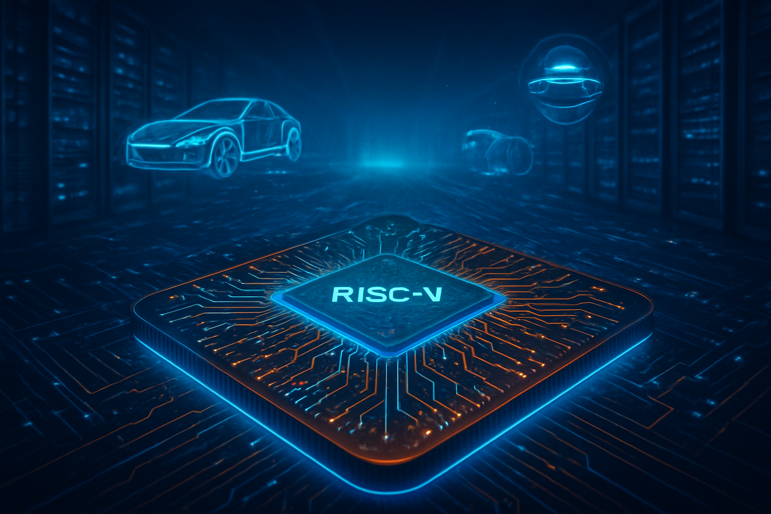
The 300mm Advantage: Engineering the Future of Edge AI
The SM1 fab is specifically engineered for 300mm (12-inch) wafer production, a significant technological leap over the older 200mm lines common in the analog chip industry. By utilizing larger wafers, Texas Instruments can produce more than double the number of chips per wafer, drastically reducing costs and improving manufacturing efficiency. The facility focuses on 28nm to 130nm specialty process nodes—the "sweet spot" for analog and embedded chips that require high reliability and long lifecycles.
Beyond the raw hardware, the Sherman site is a pioneer in "building AI with AI." The facility is one of the most automated in the world, featuring fully integrated material handling systems and the recent deployment of humanoid robots—specifically the UBTECH Walker S2—to manage repetitive tasks within the cleanroom. This AI-driven manufacturing environment generates terabytes of data every hour, which is processed in real-time to optimize wafer yields and perform predictive maintenance on sensitive lithography equipment. Initial reactions from industry analysts suggest that TI’s yields at SM1 are already exceeding industry benchmarks for a new fab, a testament to the facility's advanced automation.
Strategic Dominance: How TI’s Expansion Reshapes the Tech Hierarchy
The start of production at SM1 provides Texas Instruments with a significant competitive advantage over rivals like Analog Devices (NASDAQ: ADI) and Microchip Technology (NASDAQ: MCHP). By owning and operating its entire manufacturing flow—from wafer fabrication to assembly and test—TI can offer unparalleled supply chain transparency. This "capacity ahead of demand" strategy is designed to prevent the types of shortages that crippled the automotive industry in 2021, positioning TI as the preferred partner for tech giants and industrial leaders.
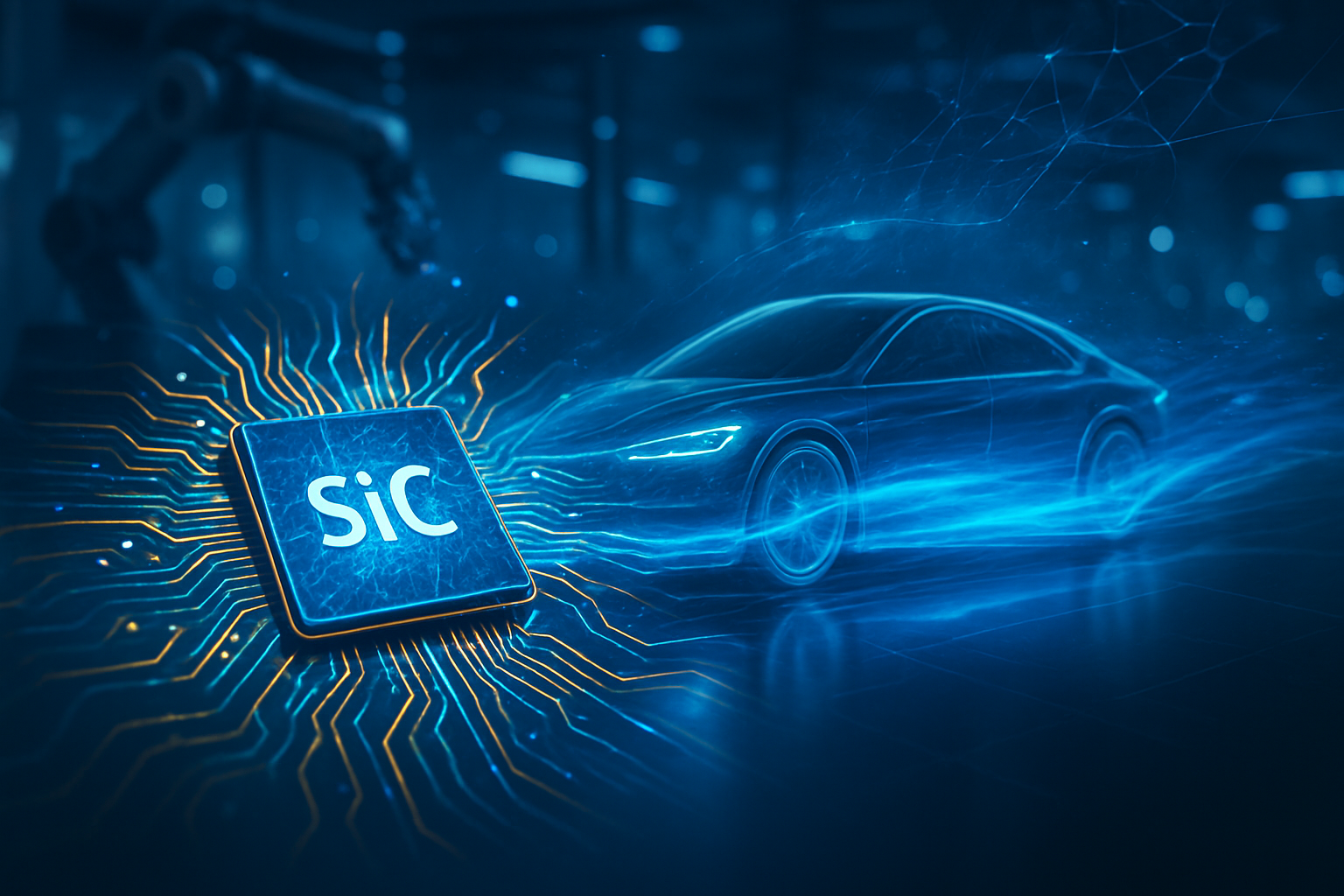
Major beneficiaries of the Sherman expansion include companies at the forefront of the AI and automotive sectors. NVIDIA (NASDAQ: NVDA) and AMD (NASDAQ: AMD) rely on TI’s high-performance power management ICs (PMICs) to regulate the extreme energy requirements of their AI data center accelerators. Similarly, Ford (NYSE: F) and other EV manufacturers are utilizing the SM1-produced chips for advanced driver-assistance systems (ADAS) and 4D imaging radar. By providing a dependable, U.S.-sourced supply of these components, TI is effectively insulating its partners from the geopolitical risks associated with offshore manufacturing.
Beyond the Silicon: The Broader Implications for National Security and AI
The Sherman mega-site is more than just a factory; it is a cornerstone of the U.S. strategy to regain semiconductor sovereignty. Supported by the CHIPS and Science Act, which provided nearly $1.6 billion in direct funding, the $60 billion investment in Sherman and other U.S. sites (including Richardson and Lehi) represents a "moonshot" for American manufacturing. The project directly addresses the vulnerabilities of the global supply chain, ensuring that the "foundational" chips required for everything from Medtronic (NYSE: MDT) medical devices to SpaceX navigation systems remain available during international crises.
In the broader context of the AI landscape, the SM1 fab is the catalyst for the transition from "Cloud AI" to "Edge AI." By mass-producing chips like the Sitara™ AM69A, which can perform complex computer vision tasks at extremely low power, TI is enabling the next generation of autonomous mobile robots and smart infrastructure. Experts believe this development is as significant as the breakthroughs in large language models, as it provides the physical infrastructure necessary for AI to interact with and navigate the real world.
The Road Ahead: Scaling the Sherman Mega-Site
While SM1 is now operational, it is only the beginning of Texas Instruments’ long-term vision. The Sherman campus is designed to house four total fabs (SM1 through SM4), with the exterior shell of SM2 already complete. As market demand for industrial and automotive electronics continues to rise, TI has the flexibility to equip and activate these additional facilities rapidly. Future upgrades are expected to focus on even tighter integration of AI within the fabrication process, potentially using machine learning to customize chip performance at the wafer level for specific client applications.
In the near term, the industry will be watching the ramp-up of the SM2 facility and the further integration of humanoid robotics into the production workflow. Challenges remain, particularly in scaling the workforce to support four massive fabs simultaneously, but TI’s early success with SM1 suggests a clear path forward. Predictions from semiconductor analysts indicate that by 2030, the Sherman site could account for nearly 20% of the world’s 300mm analog chip production capacity.
Conclusion: A New Era for American Semiconductors
The start of production at TI’s SM1 fab marks a pivotal chapter in the history of American technology. By combining a $60 billion investment with cutting-edge AI-driven manufacturing, Texas Instruments has not only secured its own future but has also fortified the supply chains that the entire global economy depends on. The facility represents a triumphant return to domestic high-volume manufacturing, proving that the U.S. can compete on both innovation and scale.
As we move into 2026, the success of the Sherman site will be a primary indicator of the health of the broader semiconductor industry. For investors and tech enthusiasts alike, the key takeaway is clear: while the software of AI captures our imagination, it is the precision-engineered silicon from fabs like SM1 that makes the revolution possible. Watch for upcoming announcements regarding the equipment of SM2 and further partnership agreements with Tier 1 automotive suppliers in the coming months.
This content is intended for informational purposes only and represents analysis of current AI and semiconductor developments.
TokenRing AI delivers enterprise-grade solutions for multi-agent AI workflow orchestration, AI-powered development tools, and seamless remote collaboration platforms.
For more information, visit https://www.tokenring.ai/.