Tag: Backside Power Delivery

  • The Power Flip: How Backside Delivery Is Saving the AI Revolution in the Angstrom Era

    The Power Flip: How Backside Delivery Is Saving the AI Revolution in the Angstrom Era

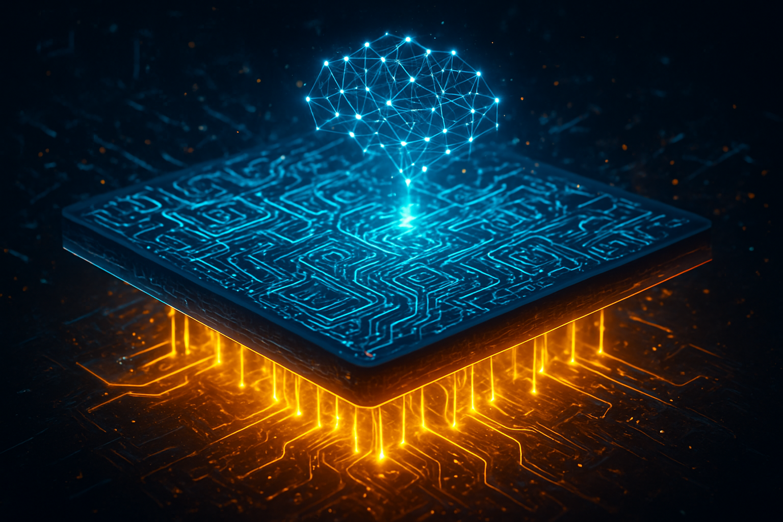
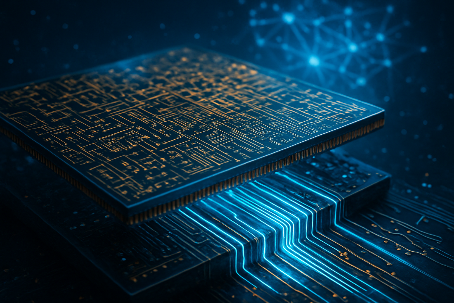
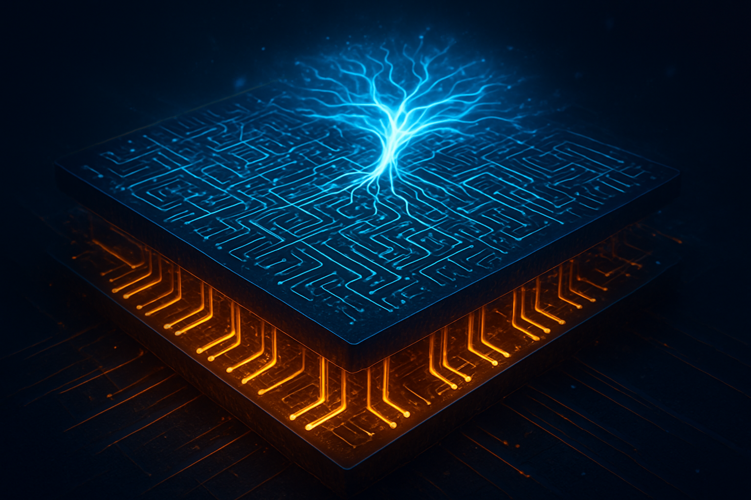
    As the artificial intelligence boom continues to strain the physical limits of silicon, a radical architectural shift has moved from the laboratory to the factory floor. As of January 2026, the semiconductor industry has officially entered the "Angstrom Era," marked by the high-volume manufacturing of Backside Power Delivery Network (BSPDN) technology. This breakthrough—decoupling power routing from signal routing—is proving to be the "secret sauce" required to sustain the multi-kilowatt power demands of next-generation AI accelerators.

    The significance of this transition cannot be overstated. For decades, chips were built like houses where the plumbing and electrical wiring were crammed into the ceiling, competing with the living space. By moving the "electrical grid" to the basement—the back of the wafer—chipmakers are drastically reducing interference, lowering heat, and allowing for unprecedented transistor density. Leading the charge are Intel Corporation (NASDAQ: INTC) and Taiwan Semiconductor Manufacturing Company Limited (NYSE: TSM), whose competing implementations are currently reshaping the competitive landscape for AI giants like Nvidia (NASDAQ: NVDA) and Advanced Micro Devices (NASDAQ: AMD).

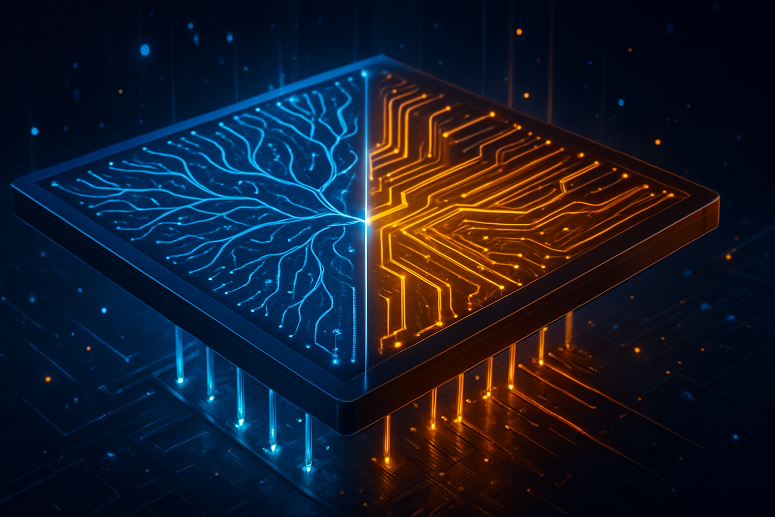
    The Technical Duel: PowerVia vs. Super Power Rail

    At the heart of this revolution are two distinct engineering philosophies. Intel, having successfully navigated its "five nodes in four years" roadmap, is currently shipping its Intel 18A node in high volume. The cornerstone of 18A is PowerVia, which uses "nano-through-silicon vias" (nTSVs) to bridge the power network from the backside to the transistor layer. By being the first to bring BSPDN to market, Intel has achieved a "first-mover" advantage that its CEO, Pat Gelsinger, claims provides a 6% frequency gain and a staggering 30% reduction in voltage droop (IR drop) for its new "Panther Lake" processors.

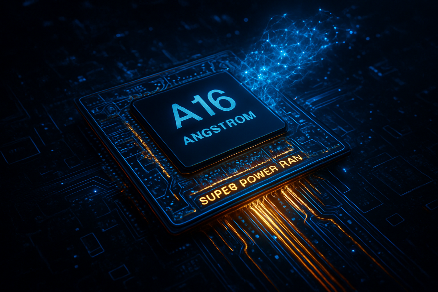
    In contrast, TSMC (NYSE: TSM) has taken a more aggressive, albeit slower-to-market, approach with its Super Power Rail (SPR) technology. While TSMC’s current 2nm (N2) node focuses on the transition to Gate-All-Around (GAA) transistors, its upcoming A16 (1.6nm) node will debut SPR in the second half of 2026. Unlike Intel’s nTSVs, TSMC’s Super Power Rail connects directly to the transistor’s source and drain. This direct-contact method is technically more complex to manufacture—requiring extreme wafer thinning—but it promises an additional 10% speed boost and higher transistor density than Intel's current 18A implementation.

    The primary benefit for both approaches is the elimination of routing congestion. In traditional front-side delivery, power wires and signal wires "fight" for the same metal layers, leading to a "logistical nightmare" of interference. By moving power to the back, the front side is de-cluttered, allowing for a 5-10% improvement in cell utilization. For AI researchers, this means more compute logic can be packed into the same square millimeter, effectively extending the life of Moore’s Law even as we approach atomic-scale limits.

    Shifting Alliances in the AI Foundry Wars

    This technological divergence is causing a strategic reshuffle among the world's most powerful AI companies. Nvidia (NASDAQ: NVDA), the reigning king of AI hardware, is preparing its Rubin (R100) architecture for a late 2026 launch. The Rubin platform is expected to be the first major GPU to utilize TSMC’s A16 node and Super Power Rail, specifically to handle the 1.8kW+ power envelopes required by frontier models. However, the high cost of TSMC’s A16 wafers—estimated at $30,000 each—has led Nvidia to evaluate Intel’s 18A as a potential secondary source, a move that would have been unthinkable just three years ago.

    Meanwhile, Microsoft (NASDAQ: MSFT) and Amazon (NASDAQ: AMZN) have already placed significant bets on Intel’s 18A node for their internal AI silicon projects, such as the Maia 2 and Trainium 3 chips. By leveraging Intel's PowerVia, these hyperscalers are seeking better performance-per-watt to lower the astronomical total cost of ownership (TCO) associated with running massive data centers. Alphabet Inc. (NASDAQ: GOOGL), through its Google Cloud division, is also pushing the limits with its TPU v7 "Ironwood", focusing on a "Rack-as-a-Unit" design that complements backside power with 400V DC distribution systems.

    The competitive implication is clear: the foundry business is no longer just about who can make the smallest transistor, but who can deliver the most efficient power. Intel’s early lead in BSPDN has allowed it to secure design wins that are critical for its "Systems Foundry" pivot, while TSMC’s density advantage remains the preferred choice for those willing to pay a premium for the absolute peak of performance.

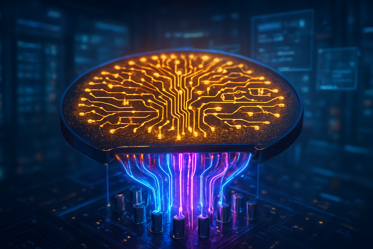
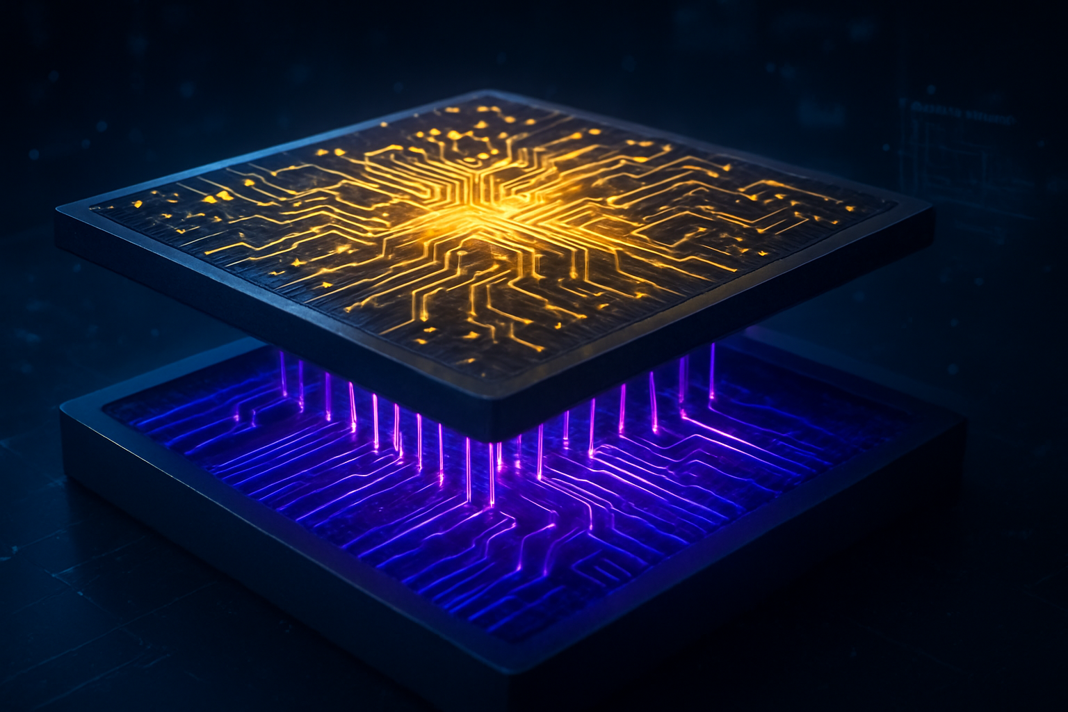
    Beyond the Transistor: The Thermal and Energy Crisis

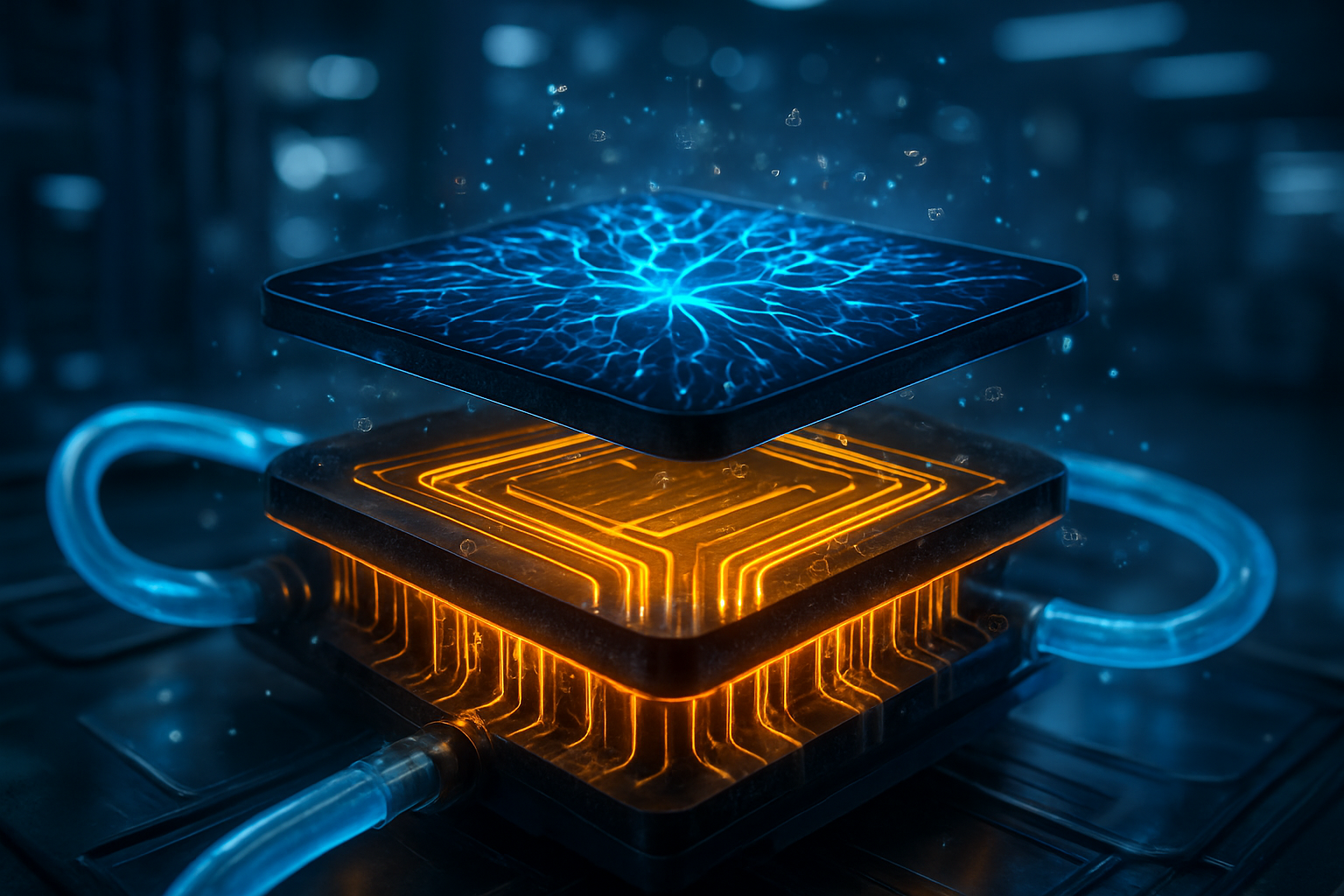
    While backside power delivery solves the "wiring" problem, it has inadvertently triggered a new crisis: thermal management. In early 2026, industry data suggests that chip "hot spots" are nearly 45% hotter in BSPDN designs than in previous generations. Because the transistor layer is now sandwiched between two dense networks of wiring, heat is effectively trapped within the silicon. This has forced a mandatory shift toward liquid cooling for all high-end AI deployments.

    This development fits into a broader trend of "forced evolution" in the AI landscape. As models grow, the energy required to train them has become a geopolitical concern. BSPDN is a vital tool for efficiency, but it is being deployed against a backdrop of diminishing returns. The $500 billion annual investment in AI infrastructure is increasingly scrutinized, with analysts at firms like Broadcom (NASDAQ: AVGO) warning that the industry must pivot from raw "TFLOPS" (Teraflops) to "Inference Efficiency" to avoid an investment bubble.

    The move to the backside is reminiscent of the transition from 2D Planar transistors to 3D FinFETs a decade ago. It is a fundamental architectural shift that will define the next ten years of computing. However, unlike the FinFET transition, the BSPDN era is defined by the needs of a single vertical: High-Performance Computing (HPC) and AI. Consumer devices like the Apple (NASDAQ: AAPL) iPhone 18 are expected to adopt these technologies eventually, but for now, the bleeding edge is reserved for the data center.

    Future Horizons: The 1,000-Watt Barrier and Beyond

    Looking ahead to 2027 and 2028, the industry is already eyeing the next frontier: "Inside-the-Silicon" cooling. To manage the heat generated by BSPDN-equipped chips, researchers are piloting microfluidic channels etched directly into the interposers. This will be essential as AI accelerators move toward 2kW and 3kW power envelopes. Intel has already announced its 14A node, which will further refine PowerVia, while TSMC is working on an even more advanced version of Super Power Rail for its A10 (1nm) process.

    The challenges remain daunting. The manufacturing complexity of BSPDN has pushed wafer prices to record highs, and the yields for these advanced nodes are still stabilizing. Experts predict that the cost of developing a single cutting-edge AI chip could exceed $1 billion by 2027, potentially consolidating the market even further into the hands of a few "megacaps" like Meta (NASDAQ: META) and Nvidia.

    A New Foundation for Intelligence

    The transition to Backside Power Delivery marks the end of the "top-down" era of semiconductor design. By flipping the chip, Intel and TSMC have provided the electrical foundation necessary for the next leap in artificial intelligence. Intel currently holds the first-mover advantage with 18A PowerVia, proving that its turnaround strategy has teeth. Yet, TSMC’s looming A16 node suggests that the battle for technical supremacy is far from over.

    In the coming months, the industry will be watching the performance of Intel’s "Panther Lake" and the first tape-outs of TSMC's A16 silicon. These developments will determine which foundry will serve as the primary architect for the "ASI" (Artificial Super Intelligence) era. One thing is certain: in 2026, the back of the wafer has become the most valuable real estate in the world.


    This content is intended for informational purposes only and represents analysis of current AI developments.

    TokenRing AI delivers enterprise-grade solutions for multi-agent AI workflow orchestration, AI-powered development tools, and seamless remote collaboration platforms.
    For more information, visit https://www.tokenring.ai/.

  • The Silent Revolution: How Backside Power Delivery is Shattering the AI Performance Wall

    The Silent Revolution: How Backside Power Delivery is Shattering the AI Performance Wall

    The semiconductor industry has officially entered the era of Backside Power Delivery (BSPDN), a fundamental architectural shift that marks the most significant change to transistor design in over a decade. As of January 2026, the long-promised "power wall" that threatened to stall AI progress is being dismantled, not by making transistors smaller, but by fundamentally re-engineering how they are powered. This breakthrough, which involves moving the intricate web of power circuitry from the top of the silicon wafer to its underside, is proving to be the secret weapon for the next generation of AI-ready processors.

    The immediate significance of this development cannot be overstated. For years, chip designers have struggled with a "logistical nightmare" on the silicon surface, where power delivery wires and signal routing wires competed for the same limited space. This congestion led to significant electrical efficiency losses and restricted the density of logic gates. With the debut of Intel’s PowerVia and the upcoming arrival of TSMC’s Super Power Rail, the industry is seeing a leap in performance-per-watt that is essential for sustaining the massive computational demands of generative AI and large-scale inference models.

    A Technical Deep Dive: PowerVia vs. Super Power Rail

    At the heart of this revolution are two competing implementations of BSPDN: PowerVia from Intel Corporation (NASDAQ: INTC) and the Super Power Rail (SPR) from Taiwan Semiconductor Manufacturing Company (NYSE: TSM). Intel has successfully taken the first-mover advantage, with its 18A node and Panther Lake processors hitting high-volume manufacturing in late 2025 and appearing in retail systems this month. Intel’s PowerVia utilizes Nano-Through Silicon Vias (nTSVs) to connect the power network on the back of the wafer to the transistors. This implementation has reduced IR drop—the voltage droop that occurs as electricity travels through a chip—from a standard 7% to less than 1%. By clearing the power lines from the frontside, Intel has achieved a staggering 30% increase in transistor density, allowing for more complex AI engines (NPUs) to be packed into smaller footprints.

    TSMC is taking a more aggressive technical path with its Super Power Rail on the A16 node, scheduled for high-volume production in the second half of 2026. Unlike Intel’s nTSV approach, TSMC’s SPR connects the power network directly to the source and drain of the transistors. While significantly harder to manufacture, this "direct contact" method is expected to offer even higher electrical efficiency. TSMC projects that A16 will deliver a 15-20% power reduction at the same clock frequency compared to its 2nm (N2P) process. This approach is specifically engineered to handle the 1,000-watt power envelopes of future data center GPUs, effectively "shattering the performance wall" by allowing chips to sustain peak boost clocks without the electrical instability that plagued previous architectures.

    Strategic Impacts on AI Giants and Startups

    This shift in manufacturing technology is creating a new competitive landscape for AI companies. Intel’s early lead with PowerVia has allowed it to position its Panther Lake chips as the premier platform for "AI PCs," capable of running 70-billion-parameter LLMs locally on thin-and-light laptops. This poses a direct challenge to competitors who are still reliant on traditional frontside power delivery. For startups and independent AI labs, the increased density means that custom silicon—previously too expensive or complex to design—is becoming more viable, as BSPDN simplifies the physical design rules for high-performance logic.

    Meanwhile, the anticipation for TSMC’s A16 node has already sparked a gold rush among the industry’s heavyweights. Nvidia (NASDAQ: NVDA) is reportedly the anchor customer for A16, intending to use the Super Power Rail to power its 2027 "Feynman" GPU architecture. The ability of A16 to deliver stable, high-amperage power directly to the transistor source is critical for Nvidia’s roadmap, which requires increasingly massive parallel throughput. For cloud giants like Amazon (NASDAQ: AMZN) and Google (NASDAQ: GOOGL), who are developing their own internal AI accelerators (Trainium and TPU), the choice between Intel’s available 18A and TSMC’s upcoming A16 will define their infrastructure efficiency and operational costs for the next three years.

    The Broader Significance: Beyond Moore's Law

    Backside Power Delivery represents more than just a clever engineering trick; it is a paradigm shift that extends the viability of Moore’s Law. As transistors shrunk toward the 2nm and 1.6nm scales, the "wiring bottleneck" became the primary limiting factor in chip performance. By separating the power and data highways into two distinct layers, the industry has effectively doubled the available "real estate" on the chip. This fits into the broader trend of "system-technology co-optimization" (STCO), where the physical structure of the chip is redesigned to meet the specific requirements of AI workloads, which are uniquely sensitive to latency and power fluctuations.

    However, this transition is not without concerns. Moving power to the backside requires complex wafer-thinning and bonding processes that increase the risk of manufacturing defects. Thermal management also becomes more complex; while moving the power grid closer to the cooling solution can help, the extreme power density of these chips creates localized "hot spots" that require advanced liquid cooling or even diamond-based heat spreaders. Compared to previous milestones like the introduction of FinFET transistors, the move to BSPDN is arguably more disruptive because it changes the entire vertical stack of the semiconductor manufacturing process.

    The Horizon: What Comes After 18A and A16?

    Looking ahead, the successful deployment of BSPDN paves the way for the "1nm era" and beyond. In the near term, we expect to see "Backside Signal Routing," where not just power, but also some global clock and data signals are moved to the underside of the wafer to further reduce interference. Experts predict that by 2028, we will see the first true "3D-stacked" logic, where multiple layers of transistors are sandwiched between multiple layers of backside and frontside routing, leading to a ten-fold increase in AI compute density.

    The primary challenge moving forward will be the cost of these advanced nodes. The equipment required for backside processing—specifically advanced wafer bonders and thinning tools—is incredibly expensive, which may lead to a widening gap between the "compute-rich" companies that can afford 1.6nm silicon and those stuck on older, frontside-powered nodes. As AI models continue to grow in size, the ability to manufacture these high-density, high-efficiency chips will become a matter of national economic security, further accelerating the "chip wars" between global superpowers.

    Closing Thoughts on the BSPDN Era

    The transition to Backside Power Delivery marks a historic moment in computing. Intel’s PowerVia has proven that the technology is ready for the mass market today, while TSMC’s Super Power Rail promises to push the boundaries of what is electrically possible by the end of the year. The key takeaway is that the "power wall" is no longer a fixed barrier; it is a challenge that has been solved through brilliant architectural innovation.

    As we move through 2026, the industry will be watching the yields of TSMC’s A16 node and the adoption rates of Intel’s 18A-based Clearwater Forest Xeons. For the AI industry, these technical milestones translate directly into faster training times, more efficient inference, and the ability to run more sophisticated models on everyday devices. The silent revolution on the underside of the silicon wafer is, quite literally, powering the future of intelligence.


    This content is intended for informational purposes only and represents analysis of current AI developments.

    TokenRing AI delivers enterprise-grade solutions for multi-agent AI workflow orchestration, AI-powered development tools, and seamless remote collaboration platforms.
    For more information, visit https://www.tokenring.ai/.

  • The Great Flip: How Backside Power Delivery is Shattering the AI Performance Wall

    The Great Flip: How Backside Power Delivery is Shattering the AI Performance Wall

    The semiconductor industry has reached a historic inflection point as the world’s leading chipmakers—Intel, TSMC, and Samsung—officially move power routing to the "backside" of the silicon wafer. This architectural shift, known as Backside Power Delivery Network (BSPDN), represents the most significant change to transistor design in over a decade. By relocating the complex web of power-delivery wires from the top of the chip to the bottom, manufacturers are finally decoupling power from signal, effectively "flipping" the traditional chip architecture to unlock unprecedented levels of efficiency and performance.

    As of early 2026, this technology has transitioned from an experimental laboratory concept to the foundational engine of the AI revolution. With AI accelerators now pushing toward 1,000-watt power envelopes and consumer devices demanding more on-device intelligence than ever before, BSPDN has become the "lifeline" for the industry. Intel (NASDAQ: INTC) has taken an early lead with its PowerVia technology, while TSMC (NYSE: TSM) is preparing to counter with its more complex A16 process, setting the stage for a high-stakes battle over the future of high-performance computing.

    For the past fifty years, chips have been built like a house where the plumbing and the electrical wiring are all crammed into the ceiling, competing for space with the occupants. In traditional "front-side" power delivery, both signal-carrying wires and power-delivery wires are layered on top of the transistors. As transistors have shrunk to the 2nm and 1.6nm scales, this "spaghetti" of wiring has become a massive bottleneck, causing signal interference and significant voltage drops (IR drop) that waste energy and generate heat.

    Intel’s implementation, branded as PowerVia, solves this by using Nano-Through Silicon Vias (nTSVs) to route power directly from the back of the wafer to the transistors. This approach, debuted in the Intel 18A process, has already demonstrated a 30% reduction in voltage droop and a 15% improvement in performance-per-watt. By removing the power wires from the front side, Intel has also been able to pack transistors 30% more densely, as the signal wires no longer have to navigate around bulky power lines.

    TSMC’s approach, known as Super PowerRail (SPR), which is slated for mass production in the second half of 2026 on its A16 node, takes the concept even further. While Intel uses nTSVs to reach the transistor layer, TSMC’s SPR connects the power network directly to the source and drain of the transistors. This "direct-contact" method is significantly more difficult to manufacture but promises even better electrical characteristics, including an 8–10% speed gain at the same voltage and up to a 20% reduction in power consumption compared to its standard 2nm process.

    Initial reactions from the AI research community have been overwhelmingly positive. Experts at the 2026 International Solid-State Circuits Conference (ISSCC) noted that BSPDN effectively "resets the clock" on Moore’s Law. By thinning the silicon wafer to just a few micrometers to allow for backside routing, chipmakers have also inadvertently improved thermal management, as the heat-generating transistors are now physically closer to the cooling solutions on the back of the chip.

    The shift to backside power delivery is creating a new hierarchy among tech giants. NVIDIA (NASDAQ: NVDA), the undisputed leader in AI hardware, is reportedly the anchor customer for TSMC’s A16 process. While their current "Rubin" architecture pushed the limits of front-side delivery, the upcoming "Feynman" architecture is expected to leverage Super PowerRail to maintain its lead in AI training. The ability to deliver more power with less heat is critical for NVIDIA as it seeks to scale its Blackwell successors into massive, multi-die "superchips."

    Intel stands to benefit immensely from its first-mover advantage. By being the first to bring BSPDN to high-volume manufacturing with its 18A node, Intel has successfully attracted major foundry customers like Microsoft (NASDAQ: MSFT) and Amazon (NASDAQ: AMZN), both of which are designing custom AI silicon for their data centers. This "PowerVia-first" strategy has allowed Intel to position itself as a viable alternative to TSMC for the first time in years, potentially disrupting the existing foundry monopoly and shifting the balance of power in the semiconductor market.

    Apple (NASDAQ: AAPL) and AMD (NASDAQ: AMD) are also navigating this transition with high stakes. Apple is currently utilizing TSMC’s 2nm (N2) node for the iPhone 18 Pro, but reports suggest they are eyeing A16 for their 2027 "M5" and "A20" chips to support more advanced generative AI features on-device. Meanwhile, AMD is leveraging its chiplet expertise to integrate backside power into its "Instinct" MI400 series, aiming to close the performance gap with NVIDIA by utilizing the superior density and clock speeds offered by the new architecture.

    For startups and smaller AI labs, the arrival of BSPDN-enabled chips means more compute for every dollar spent on electricity. As power costs become the primary constraint for AI scaling, the 15-20% efficiency gains provided by backside power could be the difference between a viable business model and a failed venture. The competitive advantage will likely shift toward those who can most quickly adapt their software to take advantage of the higher clock speeds and increased core counts these new chips provide.

    Beyond the technical specifications, backside power delivery represents a fundamental shift in the broader AI landscape. We are moving away from an era where "more transistors" was the only metric that mattered, into an era of "system-level optimization." BSPDN is not just about making transistors smaller; it is about making the entire system—from the power supply to the cooling unit—more efficient. This mirrors previous milestones like the introduction of FinFET transistors or Extreme Ultraviolet (EUV) lithography, both of which were necessary to keep the industry moving forward when physical limits were reached.

    The environmental impact of this technology cannot be overstated. With data centers currently consuming an estimated 3-4% of global electricity—a figure projected to rise sharply due to AI demand—the efficiency gains from BSPDN are a critical component of the tech industry’s sustainability goals. A 20% reduction in power at the chip level translates to billions of kilowatt-hours saved across global AI clusters. However, this also raises concerns about "Jevons' Paradox," where increased efficiency leads to even greater demand, potentially offsetting the environmental benefits as companies simply build larger, more power-hungry models.

    There are also significant geopolitical implications. The race to master backside power delivery has become a centerpiece of national industrial policies. The U.S. government’s support for Intel’s 18A progress and the Taiwanese government’s backing of TSMC’s A16 development highlight how critical this technology is for national security and economic competitiveness. Being the first to achieve high yields on BSPDN nodes is now seen as a marker of a nation’s technological sovereignty in the age of artificial intelligence.

    Comparatively, the transition to backside power is being viewed as more disruptive than the move to 3D stacking (HBM). While HBM solved the "memory wall," BSPDN is solving the "power wall." Without it, the industry would have hit a hard ceiling where chips could no longer be cooled or powered effectively, regardless of how many transistors could be etched onto the silicon.

    Looking ahead, the next two years will see the integration of backside power delivery with other emerging technologies. The most anticipated development is the combination of BSPDN with Complementary Field-Effect Transistors (CFETs). By stacking n-type and p-type transistors on top of each other and powering them from the back, experts predict another 50% jump in density by 2028. This would allow for smartphone-sized devices with the processing power of today’s high-end workstations.

    In the near term, we can expect to see "backside signaling" experiments. Once the power is moved to the back, the front side of the chip is left entirely for signal routing. Researchers are already looking into moving some high-speed signal lines to the backside as well, which could further reduce latency and increase bandwidth for AI-to-AI communication. However, the primary challenge remains manufacturing yield. Thinning a wafer to the point where backside power is possible without destroying the delicate transistor structures is an incredibly precise process that will take years to perfect for mass production.

    Experts predict that by 2030, front-side power delivery will be viewed as an antique relic of the "early silicon age." The future of AI silicon lies in "true 3D" integration, where power, signal, and cooling are interleaved throughout the chip structure. As we move toward the 1nm and sub-1nm eras, the innovations pioneered by Intel and TSMC today will become the standard blueprint for every chip on the planet, enabling the next generation of autonomous systems, real-time translation, and personalized AI assistants.

    The shift to Backside Power Delivery marks the end of the "flat" era of semiconductor design. By moving the power grid to the back of the wafer, Intel and TSMC have broken through a physical barrier that threatened to stall the progress of artificial intelligence. The immediate results—higher clock speeds, better thermal management, and improved energy efficiency—are exactly what the industry needs to sustain the current pace of AI innovation.

    As we move through 2026, the key metrics to watch will be the production yields of Intel’s 18A and the first samples of TSMC’s A16. While Intel currently holds the "first-to-market" crown, the long-term winner will be the company that can manufacture these complex architectures at the highest volume with the fewest defects. This transition is not just a technical upgrade; it is a total reimagining of the silicon chip that will define the capabilities of AI for the next decade.

    In the coming weeks, keep an eye on the first independent benchmarks of Intel’s Panther Lake processors and any further announcements from NVIDIA regarding their Feynman architecture. The "Great Flip" has begun, and the world of computing will never look the same.


    This content is intended for informational purposes only and represents analysis of current AI developments.

    TokenRing AI delivers enterprise-grade solutions for multi-agent AI workflow orchestration, AI-powered development tools, and seamless remote collaboration platforms.
    For more information, visit https://www.tokenring.ai/.

  • The Backside Revolution: How PowerVia and A16 Are Rewiring the Future of AI Silicon

    The Backside Revolution: How PowerVia and A16 Are Rewiring the Future of AI Silicon

    As of January 8, 2026, the semiconductor industry has reached a historic inflection point that promises to redefine the limits of artificial intelligence hardware. For decades, chip designers have struggled with a fundamental physical bottleneck: the "front-side" delivery of power, where power lines and signal wires compete for the same cramped real estate on top of transistors. Today, that bottleneck is being shattered as Backside Power Delivery (BSPD) officially enters high-volume manufacturing, led by Intel Corporation (NASDAQ: INTC) and its groundbreaking 18A process.

    The shift to backside power—marketing-branded as "PowerVia" by Intel and "Super PowerRail" by Taiwan Semiconductor Manufacturing Company (NYSE: TSM)—is more than a mere manufacturing tweak; it is a fundamental architectural reorganization of the microchip. By moving the power delivery network to the underside of the silicon wafer, manufacturers are unlocking unprecedented levels of power efficiency and transistor density. This development arrives at a critical moment for the AI industry, where the ravenous energy demands of next-generation Large Language Models (LLMs) have threatened to outpace traditional hardware improvements.

    The Technical Leap: Decoupling Power from Logic

    Intel's 18A process, which reached high-volume manufacturing at Fab 52 in Chandler, Arizona, earlier this month, represents the first commercial deployment of Backside Power Delivery at scale. The core innovation, PowerVia, works by separating the intricate web of signal wires from the power delivery lines. In traditional chips, power must "tunnel" through up to 15 layers of metal interconnects to reach the transistors, leading to significant "voltage droop" and electrical interference. PowerVia eliminates this by routing power through the back of the wafer using Nano-Through Silicon Vias (nTSVs), providing a direct, low-resistance path to the transistors.

    The technical specifications of Intel 18A are formidable. By implementing PowerVia alongside RibbonFET (Gate-All-Around) transistors, Intel has achieved a 30% reduction in voltage droop and a 6% boost in clock frequency at identical power levels compared to previous generations. More importantly for AI chip designers, the technology allows for 90% standard cell utilization, drastically reducing the "wiring congestion" that often forces engineers to leave valuable silicon area empty. This leap in logic density—exceeding 30% over the Intel 3 node—means more AI processing cores can be packed into the same physical footprint.

    Initial reactions from the semiconductor research community have been overwhelmingly positive. Dr. Arati Prabhakar, Director of the White House Office of Science and Technology Policy, noted during a recent briefing that "the successful ramp of 18A is a validation of the 'five nodes in four years' strategy and a pivotal moment for domestic advanced manufacturing." Industry experts at SemiAnalysis have highlighted that Intel’s decision to decouple PowerVia from its first Gate-All-Around node (Intel 20A) allowed the company to de-risk the technology, giving them a roughly 18-month lead over TSMC in mastering the complexities of backside thinning and via alignment.

    The Competitive Landscape: Intel’s First-Mover Advantage vs. TSMC’s A16 Response

    The arrival of 18A has sent shockwaves through the foundry market, placing Intel Corporation (NASDAQ: INTC) in a rare position of technical leadership over TSMC. Intel has already secured major 18A commitments from Microsoft (NASDAQ: MSFT) and Amazon (NASDAQ: AMZN) for their custom AI accelerators, Maieutics and Trainium 3, respectively. By being the first to offer a mature BSPD solution, Intel Foundry is positioning itself as the premier destination for "AI-first" silicon, where thermal management and power delivery are the primary design constraints.

    However, TSMC is not standing still. The world’s largest foundry is preparing its response in the form of the A16 node, scheduled for high-volume manufacturing in the second half of 2026. TSMC’s implementation, known as Super PowerRail, is technically more ambitious than Intel’s PowerVia. While Intel uses nTSVs to connect to the metal layers, TSMC’s Super PowerRail connects the power network directly to the source and drain of the transistors. This "direct-contact" approach is significantly harder to manufacture but is expected to offer an 8-10% speed increase and a 15-20% power reduction, potentially leapfrogging Intel’s performance metrics by late 2026.

    The strategic battle lines are clearly drawn. Nvidia (NASDAQ: NVDA), the undisputed leader in AI hardware, has reportedly signed on as the anchor customer for TSMC’s A16 node to power its 2027 "Feynman" GPU architecture. Meanwhile, Apple (NASDAQ: AAPL) is rumored to be taking a more cautious approach, potentially skipping A16 for its mobile chips to focus on the N2P node, suggesting that backside power is currently viewed as a premium feature specifically optimized for high-performance computing and AI data centers rather than consumer mobile devices.

    Wider Significance: Solving the AI Power Crisis

    The transition to backside power delivery is a critical milestone in the broader AI landscape. As AI models grow in complexity, the "power wall"—the limit at which a chip can no longer be cooled or supplied with enough electricity—has become the primary obstacle to progress. BSPD effectively raises this wall. By reducing IR drop (voltage loss) and improving thermal dissipation, backside power allows AI accelerators to run at higher sustained workloads without throttling. This is essential for training the next generation of "Agentic AI" systems that require constant, high-intensity compute cycles.

    Furthermore, this development marks the end of the "FinFET era" and the beginning of the "Angstrom era." The move to 18A and A16 represents a transition where traditional scaling (making things smaller) is being replaced by architectural scaling (rearranging how things are built). This shift mirrors previous milestones like the introduction of High-K Metal Gate (HKMG) or EUV lithography, both of which were necessary to keep Moore’s Law alive. In 2026, the "Backside Revolution" is the new prerequisite for remaining competitive in the global AI arms race.

    There are, however, concerns regarding the complexity and cost of these new processes. Backside power requires extremely precise wafer thinning—grinding the silicon down to a fraction of its original thickness—and complex bonding techniques. These steps increase the risk of wafer breakage and lower initial yields. While Intel has reported healthy 18A yields in the 55-65% range, the high cost of these chips may further consolidate power in the hands of "Big Tech" giants like Alphabet (NASDAQ: GOOGL) and Meta (NASDAQ: META), who are the only ones capable of affording the multi-billion dollar design and fabrication costs associated with 1.6nm and 1.8nm silicon.

    The Road Ahead: 1.4nm and the Future of AI Accelerators

    Looking toward the late 2020s, the trajectory of backside power is clear: it will become the standard for all high-performance logic. Intel is already planning its "14A" node for 2027, which will refine PowerVia with even denser interconnects. Simultaneously, Samsung Electronics (OTC: SSNLF) is preparing its SF2Z node for 2027, which will integrate its own version of BSPDN into its third-generation Gate-All-Around (MBCFET) architecture. Samsung’s entry will likely trigger a price war in the advanced foundry space, potentially making backside power more accessible to mid-sized AI startups and specialized ASIC designers.

    Beyond 2026, we expect to see "Backside Power 2.0," where manufacturers begin to move other components to the back of the wafer, such as decoupling capacitors or even certain types of memory (like RRAM). This could lead to "3D-stacked" AI chips where the logic is sandwiched between a backside power delivery layer and a front-side memory cache, creating a truly three-dimensional computing environment. The primary challenge remains the thermal density; as chips become more efficient at delivering power, they also become more concentrated heat sources, necessitating new liquid cooling or "on-chip" cooling technologies.

    Conclusion: A New Foundation for Artificial Intelligence

    The arrival of Intel’s 18A and the looming shadow of TSMC’s A16 mark the beginning of a new chapter in semiconductor history. Backside Power Delivery has transitioned from a laboratory curiosity to a commercial reality, providing the electrical foundation upon which the next decade of AI innovation will be built. By solving the "routing congestion" and "voltage droop" issues that have plagued chip design for years, PowerVia and Super PowerRail are enabling a new class of processors that are faster, cooler, and more efficient.

    The significance of this development cannot be overstated. In the history of AI, we will look back at 2026 as the year the industry "flipped the chip" to keep the promise of exponential growth alive. For investors and tech enthusiasts, the coming months will be defined by the ramp-up of Intel’s Panther Lake and Clearwater Forest processors, providing the first real-world benchmarks of what backside power can do. As TSMC prepares its A16 risk production in the first half of 2026, the battle for silicon supremacy has never been more intense—or more vital to the future of technology.


    This content is intended for informational purposes only and represents analysis of current AI developments.

    TokenRing AI delivers enterprise-grade solutions for multi-agent AI workflow orchestration, AI-powered development tools, and seamless remote collaboration platforms.
    For more information, visit https://www.tokenring.ai/.

  • Backside Power Delivery: The Secret Weapon for Sub-2nm Chip Efficiency

    Backside Power Delivery: The Secret Weapon for Sub-2nm Chip Efficiency

    As the artificial intelligence revolution enters its most demanding phase in 2026, the semiconductor industry has reached a pivotal turning point. The traditional methods of powering microchips—which have remained largely unchanged for decades—are being discarded in favor of a radical new architecture known as Backside Power Delivery (BSPDN). This shift is not merely an incremental upgrade; it is a fundamental redesign of the silicon wafer that is proving to be the "secret weapon" for the next generation of sub-2nm AI processors.

    By moving the complex network of power delivery lines from the top of the silicon wafer to its underside, chipmakers are finally breaking the "power wall" that has threatened to stall Moore’s Law. This innovation, spearheaded by industry giants Intel and TSMC, allows for significantly higher power efficiency, reduced signal interference, and a dramatic increase in logic density. For the AI industry, which is currently grappling with the immense energy demands of trillion-parameter models, BSPDN is the critical infrastructure enabling the hardware of tomorrow.

    The Great Flip: Moving Power to the Backside

    The technical transition to Backside Power Delivery represents the most significant architectural change in chip manufacturing since the introduction of FinFET transistors. Historically, both power and data signals were routed through a dense "forest" of metal layers on the front side of the wafer. As transistors shrank to the 2nm level and below, this "Front-side Power Delivery" (FSPDN) became a major bottleneck. The power lines and signal lines competed for the same limited space, leading to "IR drop"—a phenomenon where voltage is lost to resistance before it even reaches the transistors—and signal interference that hampered performance.

    Intel Corporation (NASDAQ: INTC) was the first to cross the finish line with its implementation, branded as PowerVia. Integrated into the Intel 18A (1.8nm) node, PowerVia utilizes Nano-Through Silicon Vias (nTSVs) to deliver electricity directly to the transistors from the back. This approach has already demonstrated a 30% reduction in IR droop and a roughly 6% increase in frequency at iso-power. Meanwhile, Taiwan Semiconductor Manufacturing Co. (NYSE: TSM) is preparing its Super Power Rail technology for the A16 node. Unlike Intel’s nTSVs, TSMC’s implementation uses direct contact to the source and drain, which is more complex to manufacture but promises an 8–10% speed improvement and up to 20% power reduction compared to its previous N2P node.

    The reaction from the AI research and hardware communities has been overwhelmingly positive. Experts note that while previous node transitions focused on making transistors smaller, BSPDN focuses on making them more accessible. By clearing the "congestion" on the front side of the chip, designers can now pack more logic gates and High Bandwidth Memory (HBM) interconnects into the same physical area. This "unclogging" of the chip's architecture is what allows for the extreme density required by the latest AI accelerators.

    A New Competitive Landscape for AI Giants

    The arrival of BSPDN has sparked a strategic reshuffling among the world’s most valuable tech companies. Intel’s early success with PowerVia has allowed it to secure major foundry customers who were previously exclusive to TSMC. Microsoft (NASDAQ: MSFT), for instance, has become a lead customer for Intel’s 18A process, utilizing it for its Maia 3 AI accelerators. For Microsoft, the power efficiency gains of BSPDN are vital for managing the astronomical electricity costs of its global data center footprint.

    TSMC, however, remains the dominant force in the high-end AI market. While its A16 node is not scheduled for high-volume manufacturing until the second half of 2026, NVIDIA (NASDAQ: NVDA) has reportedly secured early access for its upcoming "Feynman" architecture. NVIDIA’s current Blackwell successors already push the limits of thermal design power (TDP), often exceeding 1,000 watts. The Super Power Rail technology in A16 is seen as the only viable path to sustaining the performance leaps NVIDIA needs for its 2027 and 2028 roadmaps.

    Even Apple (NASDAQ: AAPL), which has long been TSMC’s most loyal partner, is reportedly exploring diversification. While Apple is expected to use TSMC’s N2P for the iPhone 18 Pro in late 2026, rumors suggest the company is qualifying Intel’s 18A for its entry-level M-series chips in 2027. This shift highlights how critical BSPDN has become; the competitive advantage is no longer just about who has the smallest transistors, but who can power them most efficiently.

    Breaking the Power Wall and Enabling 3D Silicon

    The broader significance of Backside Power Delivery lies in its ability to solve the thermal and energy crises currently facing the AI landscape. As AI models grow, the chips that train them require more current. In a traditional design, the heat generated by power delivery on the front side of the chip sits directly on top of the heat-generating transistors, creating a "thermal sandwich" that is difficult to cool. By moving power to the backside, the front of the chip can be more effectively cooled by direct-contact liquid cooling or advanced heat sinks.

    This architectural shift also paves the way for advanced 3D-stacked chips. In a 3D configuration, multiple layers of logic and memory are piled on top of each other. Previously, getting power to the middle layers of such a stack was a logistical nightmare. BSPDN provides a blueprint for "sandwiching" power and cooling between logic layers, which many believe is the only way to eventually achieve "brain-scale" computing.

    However, the transition is not without its concerns. The manufacturing process for BSPDN requires extreme wafer thinning—grinding the silicon down to just a few micrometers—and complex wafer-to-wafer bonding. This increases the risk of manufacturing defects and could lead to higher initial costs for AI startups. There is also the concern of "vendor lock-in," as the design tools required for Intel’s PowerVia and TSMC’s Super Power Rail are not fully interchangeable, forcing chip designers to choose a side early in the development cycle.

    The Road to 1nm and Beyond

    Looking ahead, the successful deployment of BSPDN in 2026 is just the beginning. Experts predict that by 2028, backside power will be standard across all high-performance computing (HPC) and mobile chips. The next frontier will be the integration of optical interconnects directly onto the backside of the wafer, allowing chips to communicate via light rather than electricity, further reducing heat and increasing bandwidth.

    In the near term, the industry is watching the H2 2026 ramp-up of TSMC’s A16 node. If TSMC can achieve high yields quickly, it could accelerate the release of OpenAI’s rumored custom "XPU" (eXtreme Processing Unit), which is being designed in collaboration with Broadcom (NASDAQ: AVGO) to leverage Super Power Rail for GPT-6 training clusters. The challenge remains the sheer complexity of the manufacturing process, but the rewards—chips that are 20% faster and significantly cooler—are too great for any major player to ignore.

    A Milestone in Semiconductor History

    Backside Power Delivery marks the end of the "two-dimensional" era of chip design and the beginning of a truly three-dimensional future. By decoupling the delivery of energy from the processing of data, Intel and TSMC have provided the AI industry with a new lease on life. This development will likely be remembered as the moment when the physical limits of silicon were pushed back, allowing the exponential growth of artificial intelligence to continue unabated.

    As we move through 2026, the key metrics to watch will be the production yields of TSMC’s A16 and the real-world performance of Intel’s 18A-based server chips. For the first time in years, the "how" of chip manufacturing is just as important as the "how small." The secret weapon for sub-2nm efficiency is no longer a secret—it is the new foundation of the digital world.


    This content is intended for informational purposes only and represents analysis of current AI developments.

    TokenRing AI delivers enterprise-grade solutions for multi-agent AI workflow orchestration, AI-powered development tools, and seamless remote collaboration platforms.
    For more information, visit https://www.tokenring.ai/.

  • The Angstrom Era Arrives: How Intel’s PowerVia and 18A Are Rewriting the Rules of AI Silicon

    The Angstrom Era Arrives: How Intel’s PowerVia and 18A Are Rewriting the Rules of AI Silicon

    The semiconductor industry has officially entered a new epoch. As of January 1, 2026, the transition from traditional transistor layouts to the "Angstrom Era" is no longer a roadmap projection but a physical reality. At the heart of this shift is Intel Corporation (Nasdaq: INTC) and its 18A process node, which has successfully integrated Backside Power Delivery (branded as PowerVia) into high-volume manufacturing. This architectural pivot represents the most significant change to chip design since the introduction of FinFET transistors over a decade ago, fundamentally altering how electricity reaches the billions of switches that power modern artificial intelligence.

    The immediate significance of this breakthrough cannot be overstated. By decoupling the power delivery network from the signal routing layers, Intel has effectively solved the "routing congestion" crisis that has plagued chip designers for years. As AI models grow exponentially in complexity, the hardware required to run them—GPUs, NPUs, and specialized accelerators—demands unprecedented current densities and signal speeds. The successful deployment of 18A provides a critical performance-per-watt advantage that is already reshaping the competitive landscape for data center infrastructure and edge AI devices.

    The Technical Architecture of PowerVia: Flipping the Script on Silicon

    For decades, microchips were built like a house where the plumbing and electrical wiring were all crammed into the same narrow crawlspace as the data cables. In traditional "front-side" power delivery, both power and signal wires are layered on top of the transistors. As transistors shrunk, these wires became so densely packed that they interfered with one another, leading to electrical resistance and "IR drop"—a phenomenon where voltage decreases as it travels through the chip. Intel’s PowerVia solves this by moving the entire power distribution network to the back of the silicon wafer. Using "Nano-TSVs" (Through-Silicon Vias), power is delivered vertically from the bottom, while the front-side metal layers are dedicated exclusively to signal routing.

    This separation provides a dual benefit: it eliminates the "spaghetti" of wires that causes signal interference and allows for significantly thicker, less resistive power rails on the backside. Technical specifications from the 18A node indicate a 30% reduction in IR drop, ensuring that transistors receive a stable, consistent voltage even under the massive computational loads required for Large Language Model (LLM) training. Furthermore, because the front side is no longer cluttered with power lines, Intel has achieved a cell utilization rate of over 90%, allowing for a logic density improvement of approximately 30% compared to previous generation nodes like Intel 3.

    Initial reactions from the semiconductor research community have been overwhelmingly positive, with experts noting that Intel has successfully executed a "once-in-a-generation" manufacturing feat. While rivals like Taiwan Semiconductor Manufacturing Co. (NYSE: TSM) and Samsung Electronics (OTC: SSNLF) are working on their own versions of backside power—TSMC’s "Super PowerRail" on its A16 node—Intel’s early lead in high-volume manufacturing gives it a rare technical "sovereignty" in the sub-2nm space. The 18A node’s ability to deliver a 6% frequency gain at iso-power, or up to a 40% reduction in power consumption at lower voltages, sets a new benchmark for the industry.

    Strategic Shifts: Intel’s Foundry Resurgence and the AI Arms Race

    The successful ramp of 18A at Fab 52 in Arizona has profound implications for the global foundry market. For years, Intel struggled to catch up to TSMC’s manufacturing lead, but PowerVia has provided the company with a unique selling proposition for its Intel Foundry services. Major tech giants are already voting with their capital; Microsoft (Nasdaq: MSFT) has confirmed that its next-generation Maia 3 (Griffin) AI accelerators are being built on the 18A node to take advantage of its efficiency gains. Similarly, Amazon (Nasdaq: AMZN) and NVIDIA (Nasdaq: NVDA) are reportedly sampling 18A-P (Performance) silicon for future data center products.

    This development disrupts the existing hierarchy of the AI chip market. By being the first to market with backside power, Intel is positioning itself as the primary alternative to TSMC for high-end AI silicon. For startups and smaller AI labs, the increased efficiency of 18A-based chips means lower operational costs for inference and training. The strategic advantage here is clear: companies that can migrate their designs to 18A early will benefit from higher clock speeds and lower thermal envelopes, potentially allowing for more compact and powerful AI hardware in both the data center and consumer "AI PCs."

    Scaling Moore’s Law in the Era of Generative AI

    Beyond the immediate corporate rivalries, the arrival of PowerVia and the 18A node represents a critical milestone in the broader AI landscape. We are currently in a period where the demand for compute is outstripping the historical gains of Moore’s Law. Backside power delivery is one of the "miracle" technologies required to keep the industry on its scaling trajectory. By solving the power delivery bottleneck, 18A allows for the creation of chips that can handle the massive "burst" currents required by generative AI models without overheating or suffering from signal degradation.

    However, this advancement does not come without concerns. The complexity of manufacturing backside power networks is immense, requiring precision wafer bonding and thinning processes that are prone to yield issues. While Intel has reported yields in the 60-70% range for early 18A production, maintaining these levels as they scale to millions of units will be a significant challenge. Comparisons are already being made to the industry's transition from planar to FinFET transistors in 2011; just as FinFET enabled the mobile revolution, PowerVia is expected to be the foundational technology for the "AI Everywhere" era.

    The Road to 14A and the Future of 3D Integration

    Looking ahead, the 18A node is just the beginning of a broader roadmap toward 3D silicon integration. Intel has already teased its 14A node, which is expected to further refine PowerVia technology and introduce High-NA EUV (Extreme Ultraviolet) lithography at scale. Near-term developments will likely focus on "complementary FETs" (CFETs), where n-type and p-type transistors are stacked on top of each other, further increasing density. When combined with backside power, CFETs could lead to a 50% reduction in chip area, allowing for even more powerful AI cores in the same physical footprint.

    The long-term potential for these technologies extends into the realm of "system-on-wafer" designs, where entire wafers are treated as a single, interconnected compute fabric. The primary challenge moving forward will be thermal management; as chips become denser and power is delivered from the back, traditional cooling methods may reach their limits. Experts predict that the next five years will see a surge in liquid-to-chip cooling solutions and new thermal interface materials designed specifically for backside-powered architectures.

    A Decisive Moment for Silicon Sovereignty

    In summary, the launch of Intel 18A with PowerVia marks a decisive victory for Intel’s turnaround strategy and a pivotal moment for the technology industry. By being the first to successfully implement backside power delivery in high-volume manufacturing, Intel has reclaimed a seat at the leading edge of semiconductor physics. The key takeaways are clear: 18A offers a substantial leap in efficiency and performance, it has already secured major AI customers like Microsoft, and it sets the stage for the next decade of silicon scaling.

    This development is significant not just for its technical metrics, but for its role in sustaining the AI revolution. As we move further into 2026, the industry will be watching closely to see how TSMC responds with its A16 node and how quickly Intel can scale its Arizona and Ohio fabs to meet the insatiable demand for AI compute. For now, the "Angstrom Era" is here, and it is being powered from the back.


    This content is intended for informational purposes only and represents analysis of current AI developments.

    TokenRing AI delivers enterprise-grade solutions for multi-agent AI workflow orchestration, AI-powered development tools, and seamless remote collaboration platforms.
    For more information, visit https://www.tokenring.ai/.

  • The Backside Revolution: How PowerVia Propels Intel into the Lead of the AI Silicon Race

    The Backside Revolution: How PowerVia Propels Intel into the Lead of the AI Silicon Race

    As the calendar turns to late 2025, the semiconductor industry is witnessing its most profound architectural shift in over a decade. The arrival of Backside Power Delivery (BSPD), spearheaded by Intel Corporation (NASDAQ: INTC) and its proprietary PowerVia technology, has fundamentally altered the physics of chip design. By physically separating power delivery from signal routing, Intel has solved a decade-long "traffic jam" on the silicon wafer, providing a critical performance boost just as the demand for generative AI reaches its zenith.

    This breakthrough is not merely an incremental improvement; it is a total reimagining of how electricity reaches the billions of transistors that power modern AI models. While traditional chips struggle with electrical interference and "voltage drop" as they shrink, PowerVia allows for more efficient power distribution, higher clock speeds, and significantly denser logic. For Intel, this represents a pivotal moment in its "five nodes in four years" strategy, potentially reclaiming the manufacturing crown from long-time rival Taiwan Semiconductor Manufacturing Company (NYSE: TSM).

    Unclogging the Silicon Arteries: The PowerVia Advantage

    For nearly fifty years, chips have been built like a layer cake, with transistors at the bottom and all the wiring—both for data signals and power—layered on top. As transistors shrank to the "Angstrom" scale, these wires became so crowded that they began to interfere with one another. Power lines, which are relatively bulky, would block the path of delicate signal wires, leading to a phenomenon known as "crosstalk" and causing significant voltage drops (IR drop) as electricity struggled to navigate the maze. Intel’s PowerVia solves this by moving the entire power delivery network to the "backside" of the silicon wafer, leaving the "front side" exclusively for data signals.

    Technically, PowerVia achieves this through the use of nano-Through Silicon Vias (nTSVs). These are microscopic vertical tunnels that pass directly through the silicon substrate to connect the backside power layers to the transistors. This approach eliminates the need for power to travel through 10 to 20 layers of metal on the front side. By shortening the path to the transistor, Intel has successfully reduced IR drop by nearly 30%, allowing transistors to switch faster and more reliably. Initial data from Intel’s 18A node, currently in high-volume manufacturing, shows frequency gains of up to 6% at the same power level compared to traditional front-side designs.

    Beyond speed, the removal of power lines from the front side has unlocked a massive amount of "real estate" for logic. Chip designers can now pack transistors much closer together, achieving density improvements of up to 30%. This is a game-changer for AI accelerators, which require massive amounts of logic and memory to process large language models. The industry response has been one of cautious optimism followed by rapid adoption, as experts recognize that BSPD is no longer a luxury, but a necessity for the next generation of high-performance computing.

    A Two-Year Head Start: Intel 18A vs. TSMC A16

    The competitive landscape of late 2025 is defined by a rare "first-mover" advantage for Intel. While Intel’s 18A node is already powering the latest "Panther Lake" consumer chips and "Clearwater Forest" server processors, TSMC is still in the preparation phase for its own BSPD implementation. TSMC has opted to skip a basic backside delivery on its 2nm node, choosing instead to debut an even more advanced version, called Super PowerRail, on its A16 (1.6nm) process. However, A16 is not expected to reach high-volume production until the second half of 2026, giving Intel a roughly 1.5 to 2-year lead in the commercial application of this technology.

    This lead has already begun to shift the strategic positioning of major AI chip designers. Companies that have traditionally relied solely on TSMC, such as NVIDIA Corporation (NASDAQ: NVDA) and Apple Inc. (NASDAQ: AAPL), are now closely monitoring Intel's foundry yields. Intel’s 18A yields are currently reported to be stabilizing between 60% and 70%, a healthy figure for a node of this complexity. The pressure is now on TSMC to prove that its Super PowerRail—which connects power directly to the transistor’s source and drain rather than using Intel's nTSV method—will offer superior efficiency that justifies the wait.

    For the market, this creates a fascinating dynamic. Intel is using its manufacturing lead to lure high-profile foundry customers who are desperate for the power efficiency gains that BSPD provides. Microsoft Corporation (NASDAQ: MSFT) and Amazon.com, Inc. (NASDAQ: AMZN) have already signed on to use Intel’s advanced nodes for their custom AI silicon, such as the Maia 2 and Trainium 2 chips. This disruption to the existing foundry hierarchy could lead to a more diversified supply chain, reducing the industry's heavy reliance on a single geographic region for the world's most advanced chips.

    Powering the AI Infrastructure: Efficiency at Scale

    The wider significance of Backside Power Delivery cannot be overstated in the context of the global AI energy crisis. As data centers consume an ever-increasing share of the world’s electricity, the 15-20% performance-per-watt improvement offered by PowerVia is a critical sustainability tool. For hyperscale cloud providers, a 20% reduction in power consumption translates to hundreds of millions of dollars saved in cooling costs and electricity bills. BSPD is effectively "free performance" that helps mitigate the thermal throttling issues that have plagued high-wattage AI chips like NVIDIA's Blackwell series.

    Furthermore, BSPD enables a new era of "computational density." By clearing the front-side metal layers, engineers can more easily integrate High Bandwidth Memory (HBM) and implement complex chiplet architectures. This allows for larger logic dies on the same interposer, as the power delivery no longer clutters the high-speed interconnects required for chip-to-chip communication. This fits into the broader trend of "system-level" scaling, where the entire package, rather than just the individual transistor, is optimized for AI workloads.

    However, the transition to BSPD is not without its concerns. The manufacturing process is significantly more complex, requiring advanced wafer bonding and thinning techniques that increase the risk of defects. There are also long-term reliability questions regarding the thermal management of the backside power layers, which are now physically closer to the silicon substrate. Despite these challenges, the consensus among AI researchers is that the benefits far outweigh the risks, marking this as a milestone comparable to the introduction of FinFET transistors in the early 2010s.

    The Road to Sub-1nm: What Lies Ahead

    Looking toward 2026 and beyond, the industry is already eyeing the next evolution of power delivery. While Intel’s PowerVia and TSMC’s Super PowerRail are the current gold standard, research is already underway for "direct-to-gate" power delivery, which could further reduce resistance. We expect to see Intel refine its 18A process into "14A" by 2027, potentially introducing even more aggressive backside routing. Meanwhile, TSMC’s A16 will likely be the foundation for the first sub-1nm chips, where BSPD will be an absolute requirement for the transistors to function at all.

    The potential applications for this technology extend beyond the data center. As AI becomes more prevalent in "edge" devices, the power savings of BSPD will enable more sophisticated on-device AI for smartphones and wearable tech without sacrificing battery life. Experts predict that by 2028, every flagship processor in the world—from laptops to autonomous vehicles—will utilize some form of backside power delivery. The challenge for the next three years will be scaling these complex manufacturing processes to meet the insatiable global demand for silicon.

    A New Era of Silicon Sovereignty

    In summary, Backside Power Delivery represents a total architectural pivot that has arrived just in time to sustain the AI revolution. Intel’s PowerVia has provided the company with a much-needed technical edge, proving that its aggressive manufacturing roadmap was more than just marketing rhetoric. By being the first to market with 18A, Intel has forced the rest of the industry to accelerate their timelines, ultimately benefiting the entire ecosystem with more efficient and powerful hardware.

    As we look ahead to the coming months, the focus will shift from technical "proofs of concept" to high-volume execution. Watch for Intel's quarterly earnings reports and foundry updates to see if they can maintain their yield targets, and keep a close eye on TSMC’s A16 risk production milestones in early 2026. This is a marathon, not a sprint, but for the first time in a decade, the lead runner has changed, and the stakes for the future of AI have never been higher.


    This content is intended for informational purposes only and represents analysis of current AI developments.

    TokenRing AI delivers enterprise-grade solutions for multi-agent AI workflow orchestration, AI-powered development tools, and seamless remote collaboration platforms.
    For more information, visit https://www.tokenring.ai/.

  • The Silicon Frontier: TSMC’s A16 and Super Power Rail Redefine the AI Chip Race

    The Silicon Frontier: TSMC’s A16 and Super Power Rail Redefine the AI Chip Race

    As the global appetite for artificial intelligence continues to outpace existing hardware capabilities, the semiconductor industry has reached a historic inflection point. Taiwan Semiconductor Manufacturing Company (NYSE: TSM), the world’s largest contract chipmaker, has officially entered the "Angstrom Era" with the unveiling of its A16 process. This 1.6nm-class node represents more than just a reduction in transistor size; it introduces a fundamental architectural shift known as "Super Power Rail" (SPR). This breakthrough is designed to solve the physical bottlenecks that have long plagued high-performance computing, specifically the routing congestion and power delivery issues that limit the scaling of next-generation AI accelerators.

    The significance of A16 cannot be overstated. For the first time in decades, the primary driver for leading-edge process nodes has shifted from mobile devices to AI data centers. While Apple Inc. (NASDAQ: AAPL) has traditionally been the first to adopt TSMC’s newest technologies, the A16 node is being tailor-made for the massive, power-hungry GPUs and custom ASICs that fuel Large Language Models (LLMs). By moving the power delivery network to the backside of the wafer, TSMC is effectively doubling the available space for signal routing, enabling a leap in performance and energy efficiency that was previously thought to be hitting a physical wall.

    The Architecture of Angstrom: Nanosheets and Super Power Rails

    Technically, the A16 process is an evolution of TSMC’s 2nm (N2) family, utilizing second-generation Gate-All-Around (GAA) Nanosheet transistors. However, the true innovation lies in the Super Power Rail (SPR), TSMC’s proprietary implementation of Backside Power Delivery (BSPDN). In traditional chip manufacturing, both signal wires and power lines are crammed onto the front side of the silicon wafer. As transistors shrink, these wires compete for space, leading to "routing congestion" and significant "IR drop"—a phenomenon where voltage decreases as it travels through the complex web of circuitry. SPR solves this by moving the entire power delivery network to the backside of the wafer, allowing the front side to be dedicated exclusively to signal routing.

    Unlike the "PowerVia" approach currently being deployed by Intel Corporation (NASDAQ: INTC), which uses nano-Through Silicon Vias (nTSVs) to bridge the power network to the transistors, TSMC’s Super Power Rail connects the power network directly to the transistor’s source and drain. This direct-contact scheme is significantly more complex to manufacture but offers superior electrical characteristics. According to TSMC, A16 provides an 8% to 10% speed boost at the same voltage compared to its N2P process, or a 15% to 20% reduction in power consumption at the same clock speed. Furthermore, the removal of power rails from the front side allows for a logic density improvement of up to 1.1x, enabling more transistors to be packed into the same physical area.

    Initial reactions from the AI research community and industry experts have been overwhelmingly positive, though cautious regarding the manufacturing complexity. Dr. Wei-Chung Hsu, a senior semiconductor analyst, noted that "A16 is the most aggressive architectural change we’ve seen since the transition to FinFET. By decoupling power and signal, TSMC is giving chip designers a clean slate to optimize for the 1000-watt chips that the AI era demands." This sentiment is echoed by EDA (Electronic Design Automation) partners who are already racing to update their software tools to handle the unique thermal and routing challenges of backside power.

    The AI Power Play: NVIDIA and OpenAI Take the Lead

    The shift to A16 has triggered a massive realignment among tech giants. For the first decade of the smartphone era, Apple was the undisputed "anchor tenant" for every new TSMC node. However, as of late 2025, reports indicate that NVIDIA Corporation (NASDAQ: NVDA) has secured the lion's share of A16 capacity for its upcoming "Feynman" architecture GPUs, expected to arrive in 2027. These chips will be the first to leverage Super Power Rail to manage the extreme power densities required for trillion-parameter model training.

    Furthermore, the A16 era marks the entry of new players into the leading-edge foundry market. OpenAI is reportedly working with Broadcom Inc. (NASDAQ: AVGO) to design its first in-house AI inference chips on the A16 node, aiming to reduce its multi-billion dollar reliance on external hardware vendors. This move positions OpenAI not just as a software leader, but as a vertical integrator capable of competing with established silicon incumbents. Meanwhile, Advanced Micro Devices (NASDAQ: AMD) is expected to follow suit, utilizing A16 for its MI400 series to maintain parity with NVIDIA’s performance gains.

    Intel, however, remains a formidable challenger. While Samsung Electronics (KRX: 005930) has reportedly delayed its 1.4nm mass production to 2029 due to yield issues, Intel’s 14A node is on track for 2026/2027. Intel is betting heavily on ASML’s (NASDAQ: ASML) High-NA EUV lithography—a technology TSMC has notably deferred for the A16 node in favor of more mature, cost-effective standard EUV. This creates a fascinating strategic divergence: TSMC is prioritizing architectural innovation (SPR), while Intel is prioritizing lithographic precision. For AI startups and cloud providers, this competition is a boon, offering two distinct paths to sub-2nm performance and a much-needed diversification of the global supply chain.

    Beyond Moore’s Law: The Broader Implications for AI Infrastructure

    The arrival of A16 and backside power delivery is more than a technical milestone; it is a necessity for the survival of the AI boom. Current AI data centers are facing a "power wall," where the energy required to cool and power massive GPU clusters is becoming the primary constraint on growth. By delivering a 20% reduction in power consumption, A16 allows data center operators to either reduce their carbon footprint or, more likely, pack 20% more compute power into the same energy envelope. This efficiency is critical as the industry moves toward "sovereign AI," where nations seek to build their own localized data centers to protect data privacy.

    However, the transition to A16 is not without its concerns. The cost of manufacturing these "Angstrom-class" wafers is skyrocketing, with industry estimates placing the price of a single A16 wafer at nearly $50,000. This represents a significant jump from the $20,000 price point seen during the 5nm era. Such high costs could lead to a bifurcation of the tech industry, where only the wealthiest "hyperscalers" like Microsoft (NASDAQ: MSFT), Alphabet (NASDAQ: GOOGL), and Amazon (NASDAQ: AMZN) can afford the absolute cutting edge, potentially widening the gap between AI leaders and smaller startups.

    Thermal management also presents a new set of challenges. With the power delivery network moved to the back of the chip, "hot spots" are now buried under layers of metal, making traditional top-side cooling less effective. This is expected to accelerate the adoption of liquid cooling and immersion cooling technologies in AI data centers, as traditional air cooling reaches its physical limits. The A16 node is thus acting as a catalyst for innovation across the entire data center stack, from the transistor level up to the facility's cooling infrastructure.

    The Roadmap Ahead: From 1.6nm to 1.4nm and Beyond

    Looking toward the future, TSMC’s A16 is just the beginning of a rapid-fire roadmap. Risk production is scheduled to begin in early 2026, with volume production ramping up in the second half of the year. This puts the first A16-powered AI chips on the market by early 2027. Following closely behind is the A14 (1.4nm) node, which will likely integrate the High-NA EUV machines that TSMC is currently evaluating in its research labs. This progression suggests that the cadence of semiconductor innovation has actually accelerated in response to the AI gold rush, defying predictions that Moore’s Law was nearing its end.

    Near-term developments will likely focus on "3D IC" packaging, where A16 logic chips are stacked directly on top of HBM4 (High Bandwidth Memory) or other logic dies. This "System-on-Integrated-Chips" (SoIC) approach will be necessary to keep the data flowing fast enough to satisfy A16’s increased processing power. Experts predict that the next two years will see a flurry of announcements regarding "chiplet" ecosystems, as designers mix and match A16 high-performance cores with older, cheaper nodes for less critical functions to manage the soaring costs of 1.6nm silicon.

    A New Era of Compute

    TSMC’s A16 process and the introduction of Super Power Rail represent a masterful response to the unique demands of the AI era. By moving power delivery to the backside of the wafer, TSMC has bypassed the routing bottlenecks that threatened to stall chip performance, providing a clear path to 1.6nm and beyond. The shift in lead customers from mobile to AI underscores the changing priorities of the global economy, as the race for compute power becomes the defining competition of the 21st century.

    As we look toward 2026 and 2027, the industry will be watching two things: the yield rates of TSMC’s SPR implementation and the success of Intel’s High-NA EUV strategy. The duopoly between TSMC and Intel at the leading edge will provide the foundation for the next generation of AI breakthroughs, from real-time video generation to autonomous scientific discovery. While the costs are higher than ever, the potential rewards of Angstrom-class silicon ensure that the silicon frontier will remain the most watched space in technology for years to come.


    This content is intended for informational purposes only and represents analysis of current AI developments.

    TokenRing AI delivers enterprise-grade solutions for multi-agent AI workflow orchestration, AI-powered development tools, and seamless remote collaboration platforms.
    For more information, visit https://www.tokenring.ai/.