Tag: Blackwell

  • NVIDIA Blackwell B200 and GB200 Chips Enter Volume Production: Fueling the Trillion-Parameter AI Era

    NVIDIA Blackwell B200 and GB200 Chips Enter Volume Production: Fueling the Trillion-Parameter AI Era

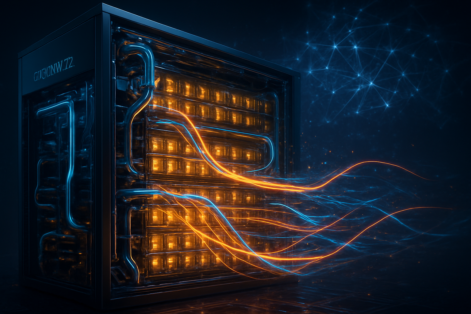
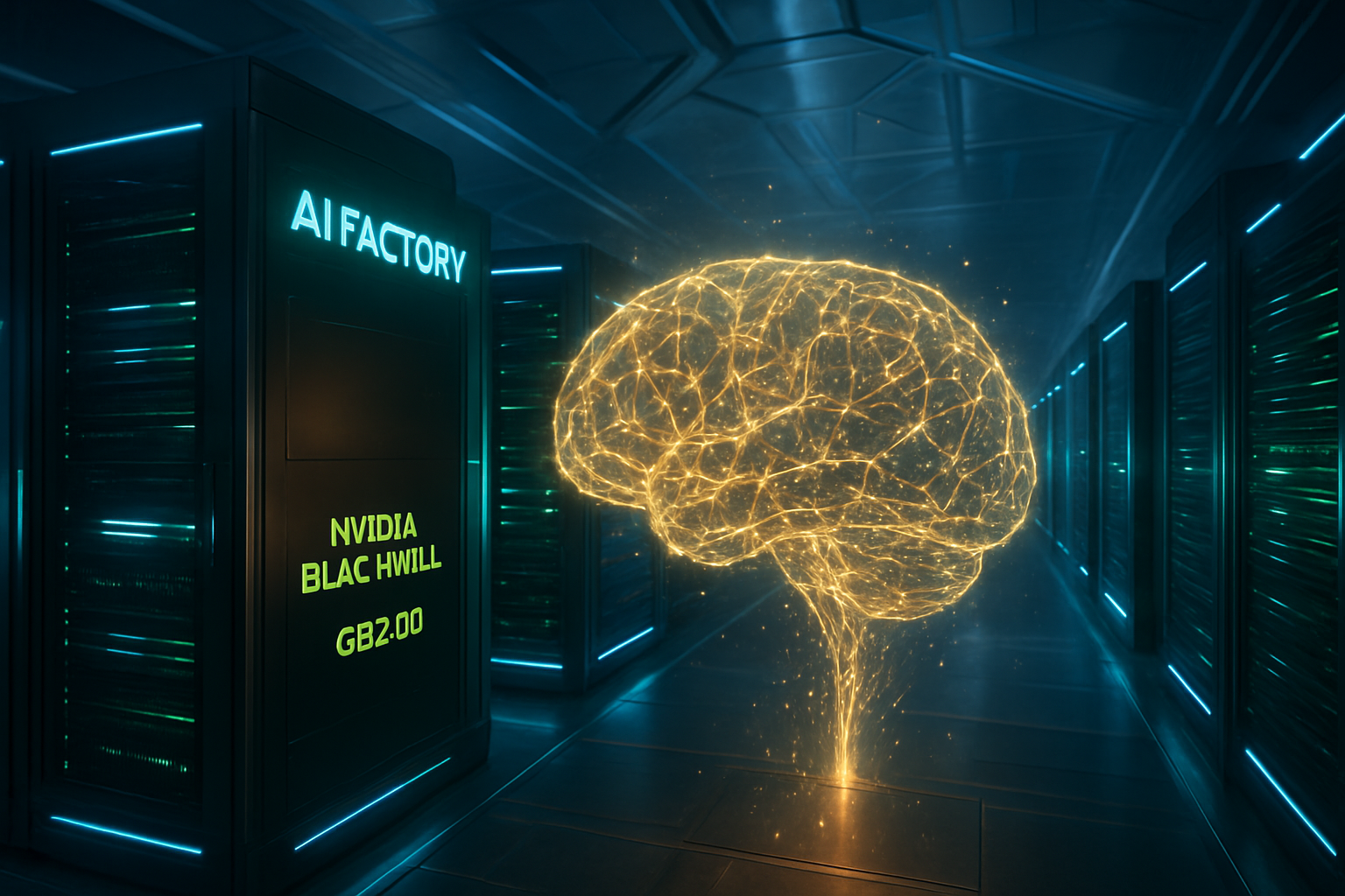
    SANTA CLARA, CA — As of February 5, 2026, the global landscape of artificial intelligence has reached a critical inflection point. NVIDIA (NASDAQ: NVDA) has officially moved its Blackwell architecture—specifically the B200 GPU and the liquid-cooled GB200 NVL72 rack system—into full-scale volume production. This transition marks the end of the "scarcity era" that defined 2024 and 2025, providing the raw computational horsepower necessary to train and deploy the next generation of frontier AI models, including OpenAI’s highly anticipated GPT-5 and its subsequent iterations.

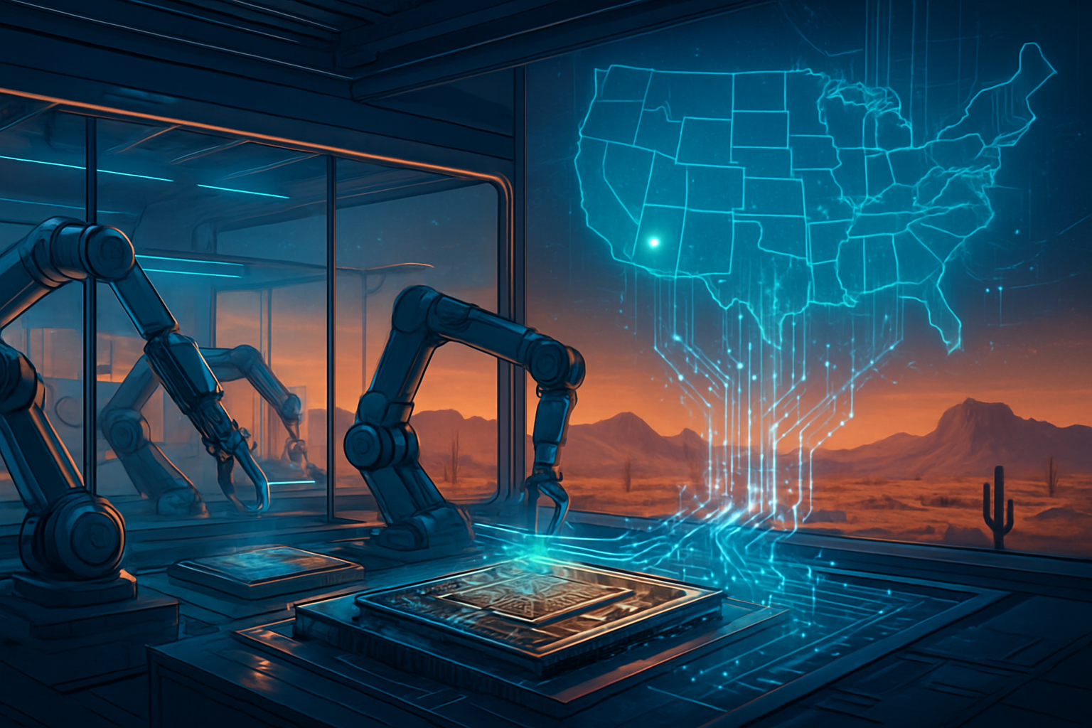
    The ramp-up in production is bolstered by a historic milestone: TSMC (NYSE: TSM) has successfully reached high-yield parity at its Fab 21 facility in Arizona. For the first time, NVIDIA’s most advanced 4NP process silicon is being produced in massive quantities on U.S. soil, significantly de-risking the supply chain for North American tech giants. With over 3.6 million units already backlogged by major cloud providers, the Blackwell era is not just an incremental upgrade; it represents the birth of the "AI Factory" as the new standard for industrial-scale intelligence.

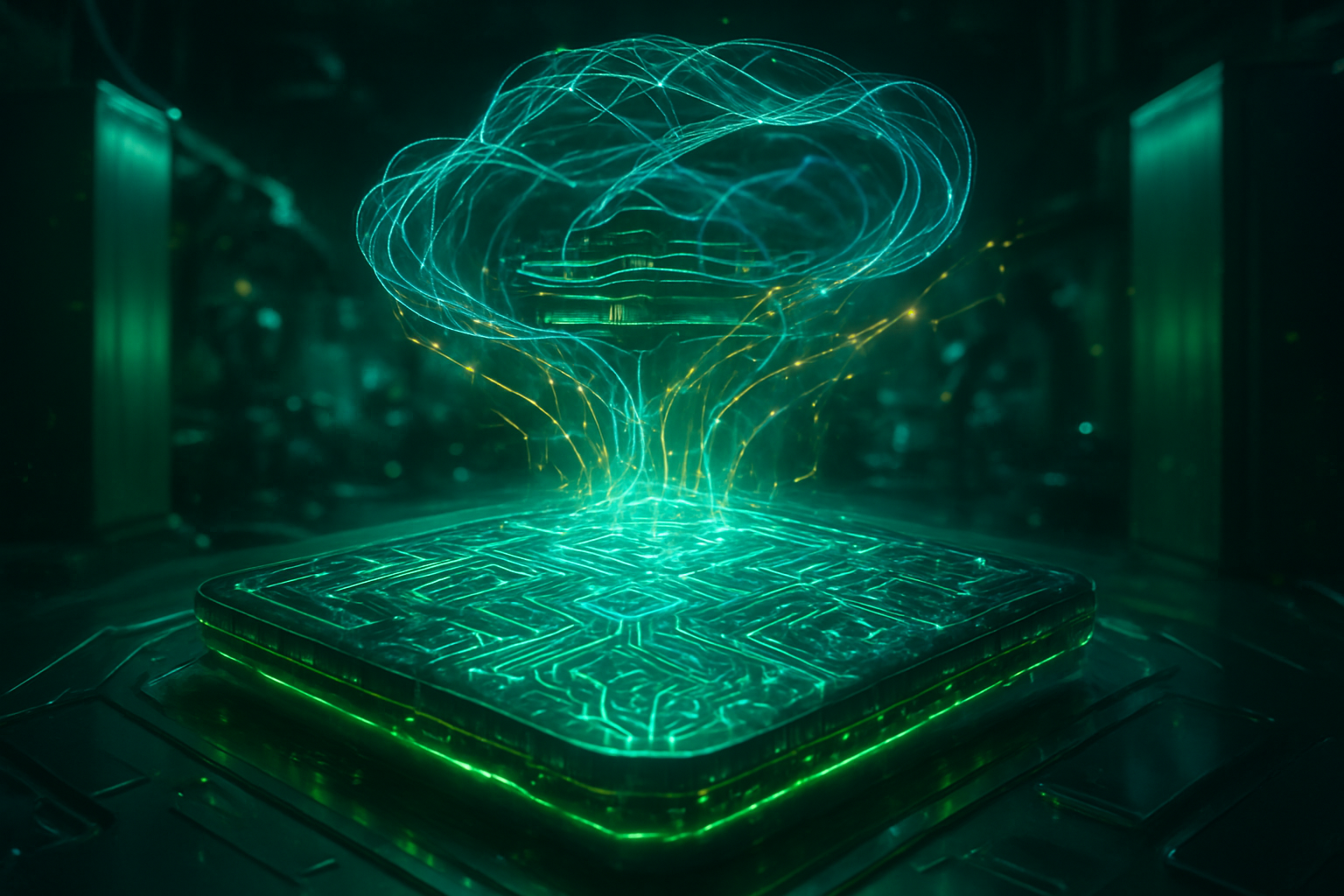
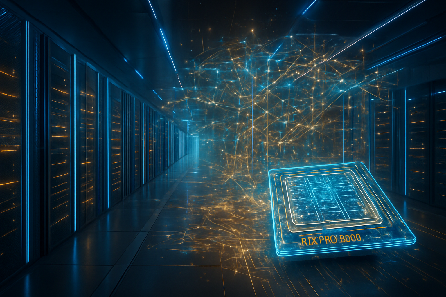
    The Blackwell B200 is a marvel of semiconductor engineering, moving away from the monolithic designs of the past toward a sophisticated dual-die chiplet architecture. Each B200 houses a staggering 208 billion transistors, effectively functioning as a single, seamless processor through a 10 TB/s interconnect. This design allows for a massive leap in memory capacity, with the standard B200 now featuring 192GB of HBM3e memory and a bandwidth of 8 TB/s. These specs represent a nearly 2.4x increase over the previous H100 "Hopper" generation, which reigned supreme throughout 2023 and 2024.

    A key technical breakthrough that has the research community buzzing is the second-generation Transformer Engine, which introduces support for FP4 precision. By utilizing 4-bit floating-point arithmetic without sacrificing significant accuracy, the Blackwell platform delivers up to 20 PFLOPS of peak performance. In practical terms, this allows researchers to serve models with 15x to 30x higher throughput than the Hopper architecture. This shift to FP4 is considered the "secret sauce" that will make the real-time operation of trillion-parameter models economically viable for the general public.

    Beyond the individual chip, the GB200 NVL72 system has redefined data center architecture. By connecting 72 Blackwell GPUs into a single unified domain via the 5th-Gen NVLink, NVIDIA has created a "rack-scale GPU" with 130 TB/s of aggregate bandwidth. This interconnect speed is crucial for models like GPT-5, which are rumored to exceed 1.8 trillion parameters. In these environments, the bottleneck is often the communication between chips; Blackwell’s NVLink 5 eliminates this, treating the entire rack as a single computational entity.

    The shift to volume production has massive implications for the "Big Three" cloud providers and the labs they support. Microsoft (NASDAQ: MSFT) has been the first to deploy tens of thousands of Blackwell units per month across its "Fairwater" AI superfactories. These facilities are specifically designed to handle the 100kW+ power density required by liquid-cooled Blackwell racks. For Microsoft and OpenAI, this infrastructure is the foundation for GPT-5, enabling the model to process context windows in the millions of tokens while maintaining the reasoning speeds required for autonomous agentic behavior.

    Amazon (NASDAQ: AMZN) and its AWS division have similarly aggressive roadmaps, recently announcing the general availability of P6e-GB200 UltraServers. AWS has notably implemented its own proprietary In-Row Heat Exchanger (IRHX) technology to manage the extreme thermal output of these chips. By providing Blackwell-tier compute at scale, AWS is positioning itself to be the primary host for the next wave of "sovereign AI" projects—national-level initiatives where countries like Japan and the UK are building their own LLMs to ensure data privacy and cultural alignment.

    The competitive advantage for companies that can secure Blackwell silicon is currently insurmountable. Startups and mid-tier AI labs that are still relying on H100 clusters are finding it difficult to compete on training efficiency. According to recent benchmarks, training a 1.8-trillion parameter model requires 8,000 Hopper GPUs and 15 MW of power, whereas the Blackwell platform can accomplish the same task with just 2,000 GPUs and 4 MW. This 4x reduction in hardware footprint and power consumption has fundamentally changed the venture capital math for AI startups, favoring those with "Blackwell-ready" infrastructure.

    Looking at the broader AI landscape, the Blackwell ramp-up signifies a transition from "brute force" scaling to "rack-scale efficiency." For years, the industry worried about the "power wall"—the idea that we would run out of electricity before we could reach AGI. Blackwell’s energy efficiency suggests that we can continue to scale model complexity without a linear increase in power consumption. This development is crucial as the industry moves toward "Agentic AI," where models don't just answer questions but perform complex, multi-step tasks in the real world.

    However, the concentration of Blackwell chips in the hands of a few tech titans has raised concerns about a growing "compute divide." While NVIDIA's increased production helps, the backlog into mid-2026 suggests that only the wealthiest organizations will have access to the peak of AI performance for the foreseeable future. This has led to renewed calls for decentralized compute initiatives and government-funded "national AI clouds" to ensure that academic researchers aren't left behind by the private sector's massive AI factories.

    The environmental impact remains a double-edged sword. While Blackwell is more efficient per TFLOP, the sheer scale of the deployments—some data centers are now crossing the 500 MW threshold—continues to put pressure on global energy grids. The industry is responding with a massive push into small modular reactors (SMRs) and direct-to-chip liquid cooling, but the "AI energy crisis" remains a primary topic of discussion at global tech summits in early 2026.

    Looking ahead, NVIDIA is not resting on its laurels. Even as the B200 reaches volume production, the first shipments of the "Blackwell Ultra" (B300) have begun, featuring an even larger 288GB HBM3e memory pool. This mid-cycle refresh is designed to bridge the gap until the arrival of the "Rubin" architecture, slated for late 2026 or early 2027. Rubin is expected to introduce even more advanced 3nm process nodes and a shift toward HBM4 memory, signaling that the pace of hardware innovation shows no signs of slowing.

    In the near term, we expect to see the "inference explosion." Now that the hardware exists to serve trillion-parameter models efficiently, we will see these capabilities integrated into every facet of consumer technology, from operating systems that can predict user needs to real-time, high-fidelity digital twins for industrial manufacturing. The challenge will shift from "how do we train these models" to "how do we govern them," as agentic AI begins to handle financial transactions, legal analysis, and healthcare diagnostics autonomously.

    The mass production of Blackwell B200 and GB200 chips represents a landmark moment in the history of computing. Much like the introduction of the first mainframes or the birth of the internet, this deployment provides the infrastructure for a new era of human productivity. NVIDIA has successfully transitioned from being a component maker to the primary architect of the world's most powerful "AI factories," solidifying its position at the center of the 21st-century economy.

    As we move through the first half of 2026, the key metric to watch will be the "token-to-watt" ratio. The true success of Blackwell will not just be measured in TFLOPS, but in how it enables AI to become a ubiquitous, affordable utility. With GPT-5 on the horizon and the hardware finally in place to support it, the next few months will likely see the most significant leaps in AI capability we have ever witnessed.


    This content is intended for informational purposes only and represents analysis of current AI developments.

    TokenRing AI delivers enterprise-grade solutions for multi-agent AI workflow orchestration, AI-powered development tools, and seamless remote collaboration platforms.
    For more information, visit https://www.tokenring.ai/.

  • Silicon Sovereignty: NVIDIA and TSMC Achieve High-Volume Blackwell Production on U.S. Soil

    Silicon Sovereignty: NVIDIA and TSMC Achieve High-Volume Blackwell Production on U.S. Soil

    In a landmark shift for the global semiconductor industry, NVIDIA (NASDAQ: NVDA) and TSMC (NYSE: TSM) have officially commenced high-volume production of the "Blackwell" AI architecture at TSMC’s Fab 21 in North Phoenix, Arizona. As of February 5, 2026, the facility has reached yield parity with TSMC’s flagship plants in Taiwan, silencing skeptics who questioned whether advanced chip manufacturing could be successfully replicated in the United States. This development marks the first time in decades that the world’s most sophisticated silicon—the literal engine of the generative AI revolution—is being fabricated domestically.

    The achievement represents more than just a logistical win; it is a geopolitical insurance policy for the American AI infrastructure. For years, the concentration of 4nm and 3nm production in the Taiwan Strait was viewed as a "single point of failure" for the global economy. By successfully transitioning the Blackwell B200 and B100 GPUs to Arizona soil, NVIDIA and TSMC have provided a strategic buffer for U.S.-based cloud providers and government agencies, ensuring that the supply of the world's most powerful AI chips remains stable even amidst rising international tensions.

    Inside the Arizona Fab: The Technical Feat of 'Yield Parity'

    The successful ramp-up at Fab 21 Phase 1 is a technical masterclass in process replication. The Blackwell chips are manufactured using TSMC’s custom 4NP process, a performance-tuned variant of the 5nm (N5) family specifically optimized for the staggering 208 billion transistors found on a single Blackwell GPU. While the "first wafer" was ceremonially signed by NVIDIA CEO Jensen Huang and TSMC executives in October 2025, the real breakthrough occurred in late January 2026, when internal audits confirmed that silicon yields—the percentage of functional chips per wafer—had reached the high-80% to low-90% range, matching the efficiency of TSMC’s primary Tainan facilities.

    This technical achievement is significant because advanced chip manufacturing is notoriously sensitive to local environmental factors, including water purity, vibration, and labor expertise. To bridge the gap, TSMC deployed a "copy-exactly" strategy, rotating thousands of American engineers through its Taiwan headquarters while flying in specialized technicians to Phoenix. Industry experts note that Blackwell’s dual-die design, which connects two high-performance chips via a 10 TB/s interconnect, leaves almost no margin for error during the lithography process. Reaching parity on such a complex architecture is a validation of the "reindustrialization" of the American desert.

    However, a critical technical nuance remains: the "Taiwan Loop." While the silicon wafers are now fabricated in Arizona, they must still be shipped back to Taiwan for CoWoS (Chip-on-Wafer-on-Substrate) advanced packaging. This final step, where the GPU is bonded to High Bandwidth Memory (HBM3e), is currently the primary bottleneck in the AI supply chain. Although TSMC has announced plans to bring advanced packaging to Arizona through a partnership with Amkor Technology (NASDAQ: AMKR), that domestic loop is not expected to be fully closed until late 2027.

    Hyperscale Hunger: How 'Made in USA' Reshapes the AI Market

    The shift to domestic production has immediate strategic implications for the "Magnificent Seven" tech giants. Microsoft (NASDAQ: MSFT), Alphabet (NASDAQ: GOOGL), and Meta Platforms (NASDAQ: META) have collectively pledged over $400 billion in capital expenditures for 2026, much of which is earmarked for Blackwell clusters. The availability of U.S.-fabricated chips allows these companies to claim a more secure and ethically "onshored" supply chain, which is becoming a requirement for high-level government and defense AI contracts.

    Despite this supply-side victory, the market remains volatile. As of early February 2026, NVIDIA’s stock has faced a "reality check" repricing, falling to a year-to-date low of approximately $172 per share. This dip is attributed to broader sector contagion—led by a weak earnings guide from rival AMD (NASDAQ: AMD)—and emerging concerns that the massive infrastructure spend by cloud providers may take longer to yield a return on investment (ROI). Furthermore, a recent report in the Financial Times alleging that specific NVIDIA optimizations were utilized by the Chinese firm DeepSeek has sparked fears of even tighter export controls, potentially complicating the global distribution of these Arizona-made chips.

    For startups and mid-tier AI labs, the Arizona facility provides a glimmer of hope for shorter lead times. Previously, the wait for Blackwell H100 or B200 units could exceed 52 weeks. With Fab 21 now in high-volume mode, analysts predict that wait times could stabilize to under 20 weeks by mid-2026, lowering the barrier to entry for smaller companies attempting to train frontier-class models.

    The CHIPS Act Legacy and the Future of Sovereign AI

    The success of the Blackwell Arizona rollout is being hailed as the ultimate validation of the CHIPS and Science Act. TSMC’s Arizona project, supported by $6.6 billion in direct federal grants and over $5 billion in loans, was long criticized as a potential "white elephant." Today, it stands as the cornerstone of America's sovereign AI strategy. By de-risking the fabrication process, the U.S. has effectively decoupled the production of its most vital technology from the immediate geographical risks of the Pacific.

    In comparison to previous milestones, such as the initial 5nm transition in 2020, the Arizona Blackwell ramp-up is a different kind of breakthrough. It is not about a new process node—the 4NP technology is well-understood—but about the mobility of advanced manufacturing. The ability to move a "cutting-edge" process across the ocean and maintain yield parity within two years suggests that the global semiconductor map is being redrawn. This move toward "technological regionalism" is likely to be emulated by the European Union and Japan as they seek to build their own sovereign AI stacks.

    However, concerns persist regarding the "dilution of margins." TSMC has guided for a 3–4% gross margin impact in 2026 due to the higher operating costs of U.S. fabs, including labor, energy, and environmental compliance. Whether the market is willing to pay a "security premium" for U.S.-made chips remains to be seen, but for now, the strategic value appears to outweigh the operational overhead.

    The Road to 2nm: What's Next for the Phoenix Cluster?

    The Blackwell milestone is only the beginning for the Arizona "Silicon Desert." On January 15, 2026, TSMC Chairman C.C. Wei announced that the schedule for the second Arizona fab has been accelerated. This second facility is slated to produce 2nm (N2) technology—the next generation of silicon—with equipment installation expected to begin in late 2026 and mass production in 2027. This acceleration is a direct response to the insatiable demand for even more efficient AI training hardware.

    Looking forward, the industry is watching for the emergence of the "Rubin" architecture, NVIDIA’s successor to Blackwell. While Blackwell currently dominates the conversation, rumors from supply chain insiders suggest that the first Rubin test wafers could appear in Arizona as early as 2027. The ultimate goal is a fully vertical U.S. supply chain where the silicon is fabricated, packaged, and assembled into server racks without ever leaving the North American continent.

    The primary challenge remaining is the workforce. While yield parity has been achieved, maintaining it at the 2nm scale will require an even more specialized labor pool. The ongoing collaboration between TSMC, the U.S. government, and local universities will be the deciding factor in whether Phoenix becomes a permanent global hub or remains a subsidized outpost of the Taiwanese ecosystem.

    A New Chapter in the History of Computing

    The successful production of Blackwell wafers in Arizona is a watershed moment in the history of computing. It marks the end of the "Offshore Era," where the world’s most advanced hardware was exclusively the product of a fragile, globalized supply chain. As of February 2026, the United States has reclaimed a seat at the table of leading-edge manufacturing, ensuring that the foundational layers of the AI era are built on stable ground.

    The key takeaway for investors and industry watchers is that the "AI bottleneck" has officially shifted. It is no longer a question of whether the world can make enough chips, but whether the software and energy infrastructure can keep up with the sheer volume of silicon now flowing out of both Taiwan and Arizona. In the coming months, all eyes will be on the Amkor packaging facility and the progress of Fab 21’s Phase 2, as the U.S. attempts to finish the job it started with the CHIPS Act.

    For now, the signed Blackwell wafer sitting in TSMC’s Phoenix headquarters serves as a powerful symbol: the future of AI is no longer just "Designed in California"—it is increasingly "Made in Arizona."


    This content is intended for informational purposes only and represents analysis of current AI developments.

    TokenRing AI delivers enterprise-grade solutions for multi-agent AI workflow orchestration, AI-powered development tools, and seamless remote collaboration platforms.
    For more information, visit https://www.tokenring.ai/.

  • The Trillion-Parameter Workhorse: How NVIDIA’s Blackwell Architecture Redefined the AI Frontier

    The Trillion-Parameter Workhorse: How NVIDIA’s Blackwell Architecture Redefined the AI Frontier

    As of February 2, 2026, the artificial intelligence landscape has reached a pivotal milestone, driven largely by the massive industrial deployment of NVIDIA’s Blackwell architecture. What began as a bold promise in late 2024 has matured into the undisputed backbone of the global AI economy. The Blackwell platform, specifically the flagship GB200 NVL72, has bridged the gap between experimental large language models and the seamless, real-time "trillion-parameter" agents that now power enterprise decision-making and autonomous systems across the globe.

    The significance of the Blackwell era lies not just in its raw compute power, but in its fundamental shift from individual chips to "rack-scale" computing. By treating an entire liquid-cooled rack as a single, unified GPU, NVIDIA (NASDAQ: NVDA) has effectively bypassed the physical limits of silicon scaling. This architectural leap has provided the necessary overhead for the industry’s transition into Mixture-of-Experts (MoE) reasoning models, which require massive memory bandwidth and low-latency interconnects to function at the speeds required for human-like interaction.

    Engineering the 130 Terabyte-per-Second "Giant GPU"

    At the heart of this technological dominance is the GB200 NVL72, a liquid-cooled system that interconnects 36 Grace CPUs and 72 Blackwell GPUs. The architectural innovation starts with the Blackwell chip itself, which utilizes a dual-die design with 208 billion transistors, linked by a 10 TB/s chip-to-chip interconnect. However, the true breakthrough is the fifth-generation NVLink, which provides a staggering 1,800 GB/s (1.8 TB/s) of bidirectional bandwidth per GPU. In the NVL72 configuration, this enables all 72 GPUs to communicate as one, creating an aggregate bandwidth domain of 130 TB/s—a feat that allows models with over 27 trillion parameters to be housed and processed within a single rack.

    This capability is specifically tuned for the complexities of Mixture-of-Experts (MoE) models. Unlike traditional dense models, MoE architectures rely on sparse activation, where only a subset of "experts" is triggered for any given task. The Blackwell architecture introduces a second-generation Transformer Engine and new FP4 (4-bit floating point) precision, which doubles throughput while maintaining the accuracy of larger models. Furthermore, a dedicated hardware decompression engine accelerates data movement by up to 800 GB/s, ensuring that the "experts" are swapped into memory with zero latency, resulting in a 30x improvement in real-time throughput for trillion-parameter models compared to the previous Hopper generation.

    Initial reactions from the AI research community have shifted from awe to total dependency. Leading researchers at labs like OpenAI and Anthropic have noted that without the NVLink 5 interconnect's ability to minimize "tail latency" during MoE inference, the current generation of multi-modal, agentic AI would have been financially and technically impossible to deploy at scale. The transition to liquid cooling has also been hailed as a necessary evolution, as the GB200 racks now handle power densities of up to 120kW, offering 25 times the energy efficiency of the air-cooled H100 systems that preceded them.

    The Hyperscaler Arms Race and Sovereign AI

    The deployment of Blackwell has solidified a hierarchy among tech giants. Microsoft (NASDAQ: MSFT), Amazon (NASDAQ: AMZN), and Alphabet (NASDAQ: GOOGL) have engaged in a relentless race to secure the largest clusters of GB200 NVL72 racks. For these hyperscalers, the Blackwell architecture is more than just a performance upgrade; it is a strategic moat. By integrating Blackwell into their cloud infrastructure, these companies have been able to offer proprietary "AI Supercomputing" tiers that smaller competitors simply cannot match in terms of cost-per-token or training speed.

    Meta Platforms (NASDAQ: META) has also been a primary beneficiary, utilizing Blackwell to train and serve its Llama-4 and Llama-5 series. The ability of the NVL72 platform to handle massive MoE weights in-memory has allowed Meta to keep its open-source models competitive with closed-source offerings. Meanwhile, the emergence of "Sovereign AI"—where nations build their own domestic compute clusters—has seen countries like Saudi Arabia and Japan investing billions into Blackwell-based data centers to ensure their data and intelligence remain within their borders, further driving NVIDIA’s 90% market share in the AI accelerator space.

    The competitive implications extend beyond the chip makers. While Advanced Micro Devices (NASDAQ: AMD) has made significant strides with its Instinct MI400 series, NVIDIA’s "one-year cadence" strategy has kept rivals in a perpetual state of catch-up. Startups that built their software stacks on CUDA (NVIDIA’s parallel computing platform) are finding it increasingly difficult to switch to alternative hardware, as the optimizations for Blackwell’s FP4 and NVLink 5 are deeply integrated into the modern AI development lifecycle. This has created a "virtuous cycle" for NVIDIA, where its hardware dominance reinforces its software lock-in.

    Beyond the Transistor: A New Era of Compute Efficiency

    When viewed through the lens of the broader AI landscape, Blackwell represents the moment AI moved from "predictive text" to "active reasoning." The massive bandwidth provided by the 1,800 GB/s NVLink 5 links has solved the memory-wall problem that plagued earlier AI architectures. This has enabled the development of "agentic" systems—AI that doesn't just answer questions but can plan, execute, and monitor multi-step tasks across different software environments. The efficiency gains have also quieted some of the criticisms regarding AI's environmental impact; the 25x increase in energy efficiency means that while AI workloads have grown, the carbon footprint per inference has plummeted.

    However, this concentration of power has not been without concern. The sheer cost of a single GB200 NVL72 rack—estimated in the millions of dollars—has raised questions about the democratization of AI. There is a growing divide between the "compute-rich" and the "compute-poor," where only the top-tier corporations and nation-states can afford to train the next generation of frontier models. Comparisons are often made to the early days of the Manhattan Project or the Space Race, where the sheer scale of the infrastructure required dictates who the global power players will be.

    Despite these concerns, the impact of Blackwell on scientific research has been profound. In fields like drug discovery and climate modeling, the ability to run trillion-parameter simulations in real-time has accelerated breakthroughs that were previously decades away. The architecture has effectively turned the data center into a giant laboratory, capable of simulating complex molecular interactions or global weather patterns with a level of granularity that was unthinkable in the era of the H100.

    The Horizon: From Blackwell to Rubin

    As we look toward the latter half of 2026, the AI industry is already preparing for the next leap. NVIDIA has officially teased the "Rubin" architecture, slated for a late 2026 release. Rubin is expected to transition to a 3nm process and debut the "Vera" CPU, alongside the sixth-generation NVLink, which is rumored to double bandwidth again to 3.6 TB/s. The move to HBM4 memory will further expand the capacity of these machines to handle even more massive models, potentially pushing into the 100-trillion-parameter range.

    The near-term focus, however, remains on the refinement of Blackwell. Experts predict that the next 12 months will see a surge in "Edge Blackwell" applications, where the power of the architecture is condensed into smaller form factors for autonomous vehicles and robotics. The challenge will be managing the heat and power requirements of such high-density compute in mobile environments. Furthermore, as models become even more efficient through 4-bit and even 2-bit quantization, the software layer will need to evolve to keep pace with the hardware’s ability to process data at terabyte-per-second speeds.

    A Definitive Chapter in AI History

    NVIDIA’s Blackwell architecture will likely be remembered as the technology that industrialized artificial intelligence. By solving the interconnection bottleneck with the 1,800 GB/s NVLink and the GB200 NVL72 platform, NVIDIA did more than just release a faster chip; they redefined the unit of compute from the GPU to the data center rack. This shift has enabled the current era of trillion-parameter MoE models, providing the raw power necessary for AI to move into its reasoning and agentic phase.

    As we move further into 2026, the key developments to watch will be the first production deployments of the Rubin architecture and the continued expansion of Sovereign AI clusters. While the competition from custom hyperscaler chips and rival GPU makers continues to grow, the Blackwell platform’s integrated ecosystem of hardware, software, and networking remains the gold standard. For now, the "Blackwell Era" stands as the most significant period of compute expansion in human history, laying the foundation for whatever intelligence comes next.


    This content is intended for informational purposes only and represents analysis of current AI developments.

    TokenRing AI delivers enterprise-grade solutions for multi-agent AI workflow orchestration, AI-powered development tools, and seamless remote collaboration platforms.
    For more information, visit https://www.tokenring.ai/.

  • NVIDIA Overtakes Apple as TSMC’s Top Customer: The Dawn of the AI Utility Phase

    NVIDIA Overtakes Apple as TSMC’s Top Customer: The Dawn of the AI Utility Phase

    In a watershed moment for the global semiconductor industry, NVIDIA (NASDAQ: NVDA) has officially surpassed Apple (NASDAQ: AAPL) to become the largest revenue contributor for Taiwan Semiconductor Manufacturing Company (TSMC) (NYSE: TSM). Financial data emerging in early 2026 reveals a tectonic shift in the foundry’s client hierarchy: NVIDIA is projected to generate approximately $33 billion in revenue for TSMC this year, accounting for 22% of the total, while Apple, the long-standing "alpha" customer, is expected to contribute $27 billion, or roughly 18%.

    This reversal marks the first time in over a decade that a company other than Apple has held the top spot at the world’s premier chipmaker. The development is more than just a corporate milestone; it signals a fundamental realignment of the global economy. For the past fifteen years, the semiconductor market was largely defined by the smartphone and consumer electronics boom led by Apple. Today, that mantle has passed to the builders of artificial intelligence infrastructure, marking the definitive arrival of the "AI era" in industrial manufacturing.

    The Architecture of Dominance: Blackwell, Rubin, and the CoWoS Bottleneck

    The primary catalyst for this revenue surge is the sheer physical and technical complexity of NVIDIA’s latest silicon architectures. Unlike consumer-grade chips found in iPhones or MacBooks, which are optimized for power efficiency and mass-market costs, NVIDIA’s high-end AI accelerators like the Blackwell Ultra (GB300) and the upcoming Vera Rubin (R100) platforms are massive, high-performance systems. These chips push the boundaries of "reticle size"—the maximum area a single chip can occupy on a wafer—often requiring multiple dies to be stitched together with extreme precision. This complexity allows TSMC to command significantly higher prices per wafer compared to the smaller, more streamlined A-series chips produced for Apple.

    A critical component of this revenue growth is TSMC’s Chip on Wafer on Substrate (CoWoS) packaging technology. As AI models demand faster data throughput, the "glue" that connects GPUs with High-Bandwidth Memory (HBM) has become the industry’s most valuable bottleneck. NVIDIA has reportedly secured nearly 60% of TSMC’s entire CoWoS capacity for 2026. This advanced packaging is a high-margin service that adds a substantial layer of revenue on top of traditional wafer fabrication. By late 2026, TSMC’s CoWoS capacity is expected to reach over 100,000 wafers per month to keep pace with NVIDIA’s relentless release cycle.

    Initial reactions from the semiconductor research community suggest that NVIDIA’s move to the top spot was inevitable given the massive die sizes of the Rubin architecture. Analysts note that while Apple still ships hundreds of millions more individual chips than NVIDIA, the "value-per-wafer" for an AI accelerator is orders of magnitude higher. Industry experts believe this creates a "priority lock" where NVIDIA now gets first access to TSMC's most advanced nodes, such as the upcoming 2nm (N2) process, a privilege previously reserved almost exclusively for Apple.

    Reshaping the Tech Titan Hierarchy

    This shift has profound implications for the competitive landscape of Big Tech. For years, Apple’s dominance at TSMC gave it a strategic "moat," ensuring its products had the most efficient processors on the market before anyone else. Now, with NVIDIA as the primary revenue driver, TSMC is increasingly incentivized to prioritize the high-performance computing (HPC) requirements of AI over the low-power requirements of mobile devices. This could potentially slow the pace of performance gains in consumer hardware while accelerating the capabilities of the data centers that power AI services.

    Major AI labs and cloud providers—including Microsoft (NASDAQ: MSFT), Amazon (NASDAQ: AMZN), and Alphabet (NASDAQ: GOOGL)—stand to benefit from this alignment, as NVIDIA’s primary status ensures a steady, albeit expensive, supply of the hardware needed to scale their generative AI products. However, the high cost of NVIDIA’s Rubin platform, which targets a 10x reduction in token generation costs, creates a high barrier to entry for smaller startups. These companies must now navigate a market where the "silicon tax" is increasingly paid to a single, dominant provider that sits at the top of the manufacturing food chain.

    The strategic advantage has clearly pivoted. NVIDIA's ability to command TSMC’s roadmap means the foundry is now optimizing its future factories for "big silicon" rather than "small silicon." This transition forces competitors like AMD (NASDAQ: AMD) to compete for the remaining advanced packaging capacity, potentially tightening the supply of rival AI chips and further cementing NVIDIA’s market positioning as the de facto gatekeeper of AI compute.

    Entering the 'Utility Phase' of the AI Cycle

    Market analysts are describing this period as the transition from the "Land Grab Phase" to the "Utility Phase" of the AI cycle. During 2023 and 2024, the industry saw a frantic, speculative rush to acquire any available GPUs to avoid being left behind. In 2026, the focus has shifted toward Return on Investment (ROI) and enterprise-wide productivity. AI is no longer a peripheral experiment; it has become a core utility, as essential to modern business as electricity or high-speed internet.

    The fact that NVIDIA has overtaken Apple—a company built on consumer desire—indicates that the AI cycle is now driven by industrial necessity. This stage of the cycle requires a drastic reduction in the cost of intelligence to remain sustainable. This is why the Rubin architecture is so significant; by focusing on slashing the cost per token, NVIDIA is making it economically viable for businesses to embed AI into every layer of their software stacks. It represents a move toward the commoditization of high-level reasoning.

    Comparatively, this milestone is being likened to the moment in the early 20th century when industrial power generation surpassed residential lighting as the primary driver of the electrical grid. The sheer scale of infrastructure being built suggests that we are move past the "hype" and into a decade-long deployment phase. While concerns about an "AI bubble" persist, the hard capital expenditures flowing from the world’s most valuable companies into TSMC’s foundries suggest a long-term commitment to this technological pivot.

    The Horizon: 2nm and Beyond

    Looking ahead, the next battleground will be the transition to the 2nm (N2) process node, expected to ramp up in late 2026 and 2027. Experts predict that NVIDIA will be the lead customer for this node, utilizing "GAAFET" (Gate-All-Around Field-Effect Transistor) technology to further increase the density of its Rubin-successor chips. The challenge will not just be fabrication, but the continued scaling of HBM and advanced packaging, which remain prone to yield issues and supply chain disruptions.

    In the near term, we can expect NVIDIA to push deeper into vertical integration, perhaps offering more tailored "AI factories" that include not just the chips, but the liquid cooling and networking stacks required to run them. The goal is to move from selling components to selling entire units of "intelligence." Challenges remain, particularly regarding the massive power consumption of these new data centers and the geopolitical tensions surrounding semiconductor manufacturing in the Taiwan Strait, which remains a singular point of failure for the global AI economy.

    A New Era in Computing History

    The ascension of NVIDIA to the top of TSMC’s customer list is a historic realignment that marks the end of the mobile-first era and the beginning of the AI-first era. It underscores a shift in value from the device in our pockets to the massive, distributed intelligence engines in the cloud. NVIDIA’s $33 billion contribution to TSMC’s coffers is the ultimate proof of the industry's belief in the permanence of the AI revolution.

    As we move through 2026, the key metrics to watch will be the "cost-per-token" metrics provided by the Rubin platform and the speed at which TSMC can expand its CoWoS capacity. If NVIDIA can continue to lower the cost of AI while maintaining its lead at the foundry, it will solidify its role as the foundational utility of the 21st century. The world is no longer just buying gadgets; it is building a new kind of cognitive infrastructure, and for the first time, the numbers at the world's most important factory prove it.


    This content is intended for informational purposes only and represents analysis of current AI developments.

    TokenRing AI delivers enterprise-grade solutions for multi-agent AI workflow orchestration, AI-powered development tools, and seamless remote collaboration platforms.
    For more information, visit https://www.tokenring.ai/.

  • The Great GPU War of 2026: AMD’s MI350 Series Challenges NVIDIA’s Blackwell Hegemony

    The Great GPU War of 2026: AMD’s MI350 Series Challenges NVIDIA’s Blackwell Hegemony

    As of January 2026, the artificial intelligence landscape has transitioned from a period of desperate hardware scarcity to an era of fierce architectural competition. While NVIDIA Corporation (NASDAQ: NVDA) maintained a near-monopoly on high-end AI training for years, the narrative has shifted in the enterprise data center. The arrival of the Advanced Micro Devices, Inc. (NASDAQ: AMD) Instinct MI325X and the subsequent MI350 series has created the first genuine duopoly in the AI accelerator market, forcing a direct confrontation over memory density and inference throughput.

    The immediate significance of this battle lies in the democratization of massive-scale inference. With the release of the MI350 series, built on the cutting-edge 3nm CDNA 4 architecture, AMD has effectively neutralized NVIDIA’s traditional software moat by offering raw hardware specifications—specifically in High Bandwidth Memory (HBM) capacity—that make it mathematically more efficient to run trillion-parameter models on AMD hardware. This shift has prompted major cloud providers and enterprise leaders to diversify their silicon portfolios, ending the "NVIDIA-only" era of the AI boom.

    Technical Superiority through Memory and Precision

    The technical skirmish between AMD and NVIDIA is currently centered on two critical metrics: HBM3e density and FP4 (4-bit floating point) throughput. The AMD Instinct MI350 series, headlined by the MI355X, boasts a staggering 288GB of HBM3e memory and a peak memory bandwidth of 8.0 TB/s. This allows the chip to house massive Large Language Models (LLMs) entirely within a single GPU's memory, reducing the latency-heavy data transfers between chips that plague smaller-memory architectures. In response, NVIDIA accelerated its roadmap, releasing the Blackwell Ultra (B300) series in late 2025, which finally matched AMD’s 288GB density by utilizing 12-high HBM3e stacks.

    AMD’s generational leap from the MI300 to the MI350 is perhaps the most significant in the company’s history, delivering a 35x improvement in inference performance. Much of this gain is attributed to the introduction of native FP4 support, a precision format that allows for higher throughput without a proportional loss in model accuracy. While NVIDIA’s Blackwell architecture (B200) initially set the gold standard for FP4, AMD’s MI350 has achieved parity in dense compute performance, claiming up to 20 PFLOPS of FP4 throughput. This technical parity has turned the "Instinct vs. Blackwell" debate into a question of TCO (Total Cost of Ownership) rather than raw capability.

    Industry experts initially reacted with skepticism to AMD’s aggressive roadmap, but the mid-2025 launch of the CDNA 4 architecture proved that AMD could maintain a yearly cadence to match NVIDIA’s breakneck speed. The research community has particularly praised AMD’s commitment to open standards via ROCm 7.0. By late 2025, ROCm reached feature parity with NVIDIA’s CUDA for the vast majority of PyTorch and JAX-based workloads, effectively lowering the "switching cost" for developers who were previously locked into NVIDIA’s ecosystem.

    Strategic Realignment in the Enterprise Data Center

    The competitive implications of this hardware parity are profound for the "Magnificent Seven" and emerging AI startups. For companies like Microsoft Corporation (NASDAQ: MSFT) and Meta Platforms, Inc. (NASDAQ: META), the MI350 series provides much-needed leverage in price negotiations with NVIDIA. By deploying thousands of AMD nodes, these giants have signaled that they are no longer beholden to a single vendor. This was most notably evidenced by OpenAI's landmark 2025 deal to utilize 6 gigawatts of AMD-powered infrastructure, a move that provided the MI350 series with the ultimate technical validation.

    For NVIDIA, the emergence of a potent MI350 series has forced a shift in strategy from selling individual GPUs to selling entire "AI Factories." NVIDIA's GB200 NVL72 rack-scale systems remain the industry benchmark for large-scale training due to the superior NVLink 5.0 interconnect, which offers 1.8 TB/s of chip-to-chip bandwidth. However, AMD’s acquisition of ZT Systems, completed in 2025, has allowed AMD to compete at this system level. AMD can now deliver fully integrated, liquid-cooled racks that rival NVIDIA’s DGX systems, directly challenging NVIDIA’s dominance in the plug-and-play enterprise market.

    Startups and smaller enterprise players are the primary beneficiaries of this competition. As NVIDIA and AMD fight for market share, the cost per token for inference has plummeted. AMD has aggressively marketed its MI350 chips as providing "40% more tokens-per-dollar" than the Blackwell B200. This pricing pressure has prevented NVIDIA from further expanding its already record-high margins, creating a more sustainable economic environment for companies building application-layer AI services.

    The Broader AI Landscape: From Scarcity to Scale

    This battle fits into a broader trend of "Inference-at-Scale," where the industry’s focus has shifted from training foundational models to serving them to millions of users efficiently. In 2024, the bottleneck was getting any chips at all; in 2026, the bottleneck is the power density and cooling capacity of the data center. The MI350 and Blackwell Ultra series both push the limits of power consumption, with peak TDPs reaching between 1200W and 1400W. This has sparked a massive secondary industry in liquid cooling and data center power management, as traditional air-cooled racks can no longer support these top-tier accelerators.

    The significance of the 288GB HBM3e threshold cannot be overstated. It marks a milestone where "frontier" models—those with 500 billion to 1 trillion parameters—can be served with significantly less hardware overhead. This reduces the physical footprint of AI data centers and mitigates some of the environmental concerns surrounding AI’s energy consumption, as higher memory density leads to better energy efficiency per inference task.

    However, this rapid advancement also brings concerns regarding electronic waste and the speed of depreciation. With both NVIDIA and AMD moving to annual release cycles, high-end accelerators purchased just 18 months ago are already being viewed as legacy hardware. This "planned obsolescence" at the silicon level is a new phenomenon for the enterprise data center, requiring a complete rethink of how companies amortize their massive capital expenditures on AI infrastructure.

    Looking Ahead: Vera Rubin and the MI400

    The next 12 to 24 months will see the introduction of NVIDIA’s "Vera Rubin" architecture and AMD’s Instinct MI400. Experts predict that NVIDIA will attempt to reclaim its undisputed lead by introducing even more proprietary interconnect technologies, potentially moving toward optical interconnects to overcome the physical limits of copper. NVIDIA is expected to lean heavily into its "Grace" CPU integration, pushing the Superchip model even harder to maintain a system-level advantage that AMD’s MI350, which often relies on third-party CPUs, may struggle to match.

    AMD, meanwhile, is expected to double down on its "chiplet" advantage. The MI400 is rumored to utilize an even more modular design, allowing for customizable ratios of compute to memory. This would allow enterprise customers to order "inference-heavy" or "training-heavy" versions of the same chip, a level of flexibility that NVIDIA’s more monolithic Blackwell architecture does not currently offer. The challenge for both will remain the supply chain; while HBM shortages have eased by early 2026, the sub-3nm fabrication capacity at TSMC remains a tightly contested resource.

    A New Era of Silicon Competition

    The battle between the AMD Instinct MI350 and NVIDIA Blackwell marks the end of the first phase of the AI revolution and the beginning of a mature, competitive industry. NVIDIA remains the revenue leader, holding approximately 85% of the market share, but AMD’s projected climb to a 10-12% share by mid-2026 represents a massive shift in the data center power dynamic. The "GPU War" has successfully moved the needle from theoretical performance to practical, enterprise-grade reliability and cost-efficiency.

    As we move further into 2026, the key metric to watch will be the adoption of these chips in the "sovereign AI" sector—nationalized data centers and regional cloud providers. While the US hyperscalers have led the way, the next wave of growth for both AMD and NVIDIA will come from global markets seeking to build their own independent AI infrastructure. For the first time in the AI era, those customers truly have a choice.


    This content is intended for informational purposes only and represents analysis of current AI developments.

    TokenRing AI delivers enterprise-grade solutions for multi-agent AI workflow orchestration, AI-powered development tools, and seamless remote collaboration platforms.
    For more information, visit https://www.tokenring.ai/.

  • SK Hynix Invests $13 Billion in World’s Largest HBM Packaging Plant (P&T7) to Power NVIDIA’s Rubin Era

    SK Hynix Invests $13 Billion in World’s Largest HBM Packaging Plant (P&T7) to Power NVIDIA’s Rubin Era

    In a move that solidifies its lead in the high-stakes artificial intelligence memory race, SK Hynix (KRX: 000660) has officially announced a massive $13 billion (19 trillion won) investment to construct "P&T7," slated to be the world's largest dedicated High Bandwidth Memory (HBM) packaging and testing facility. Located in the Cheongju Technopolis Industrial Complex in South Korea, this facility is designed to serve as the global nerve center for the production of HBM4, the next-generation memory architecture required to power the most advanced AI processors on the planet.

    The announcement, formalized on January 13, 2026, marks a pivotal moment in the semiconductor industry as the demand for memory bandwidth begins to outpace traditional compute scaling. By integrating the P&T7 facility with the adjacent M15X production line, SK Hynix is creating a vertically integrated "super-fab" capable of handling everything from initial DRAM fabrication to the complex 16-layer vertical stacking required for NVIDIA (NASDAQ: NVDA) and its upcoming Rubin GPU architecture. This investment signals that the bottleneck for AI progress is no longer just the logic of the chip, but the speed and efficiency with which that chip can access data.

    The Technical Frontier: HBM4 and the Logic-Memory Merger

    The P&T7 facility is specifically engineered to overcome the daunting physical challenges of HBM4. Unlike its predecessor, HBM3E, which featured a 1024-bit interface, HBM4 doubles the interface width to 2048-bit. This leap allows for staggering bandwidths exceeding 2 TB/s per memory stack. To achieve this, SK Hynix is deploying its proprietary Advanced Mass Reflow Molded Underfill (MR-MUF) technology at P&T7. This process allows the company to stack up to 16 layers of DRAM—offering capacities of 64GB per cube—while keeping the total height within the strict 775-micrometer JEDEC standard. This requires thinning individual DRAM dies to a mere 30 micrometers, a feat of precision engineering that P&T7 is uniquely equipped to handle at scale.

    Perhaps the most significant technical shift at P&T7 is the transition of the HBM "base die." In previous generations, the base die was a standard memory component. For HBM4, the base die will be manufactured using advanced logic processes (5nm and 3nm) in collaboration with TSMC (NYSE: TSM). This effectively turns the memory stack into a semi-custom co-processor, allowing for better thermal management and lower latency. The P&T7 plant will act as the final integration point where these TSMC-made logic dies are married to SK Hynix’s high-density DRAM, representing an unprecedented level of cross-foundry collaboration.

    Initial reactions from the semiconductor research community suggest that SK Hynix’s decision to stick with MR-MUF for the initial 16-layer HBM4 rollout—rather than jumping immediately to hybrid bonding—is a strategic move to ensure high yields. While competitors are experimenting with hybrid bonding to reduce stack height, SK Hynix’s refined MR-MUF process has already demonstrated superior thermal dissipation, a critical factor for GPUs like NVIDIA’s Blackwell and Rubin that operate at extreme power densities.

    Securing the NVIDIA Pipeline: From Blackwell to Rubin

    The primary beneficiary of this $13 billion investment is NVIDIA (NASDAQ: NVDA), which has reportedly secured approximately 70% of SK Hynix's HBM4 production capacity through 2027. While SK Hynix currently dominates the supply of HBM3E for the NVIDIA Blackwell (B100/B200) family, the P&T7 facility is built with the future "Rubin" platform in mind. The Rubin GPU is expected to utilize eight stacks of HBM4, providing an astronomical 288GB of ultra-fast memory and 22 TB/s of bandwidth. This leap is essential for the next generation of LLMs, which are expected to exceed 10 trillion parameters.

    The competitive implications for other tech giants are profound. Samsung (KRX: 005930) and Micron (NASDAQ: MU) are racing to catch up, with Samsung recently passing quality tests for its own HBM4 modules. However, the sheer scale of the P&T7 facility gives SK Hynix a massive advantage in "economies of skill." By housing packaging and testing in such close proximity to the M15X fab, SK Hynix can achieve yield stabilities that are difficult for competitors with fragmented supply chains to match. For hyperscalers like Microsoft (NASDAQ: MSFT) and Meta (NASDAQ: META), who are increasingly designing their own AI silicon, SK Hynix’s P&T7 offers a blueprint for how "custom memory" will be delivered in the late 2020s.

    This investment also disrupts the traditional vendor-client relationship. The move toward logic-based base dies means SK Hynix is moving up the value chain, acting more like a boutique foundry for high-performance components rather than a bulk commodity memory supplier. This strategic positioning makes them an indispensable partner for any company attempting to compete at the frontier of AI training and inference.

    The Broader AI Landscape: Overcoming the Memory Wall

    The P&T7 announcement is a direct response to the "Memory Wall"—the growing disparity between how fast a processor can compute and how fast data can be moved into that processor. As AI models grow in complexity, the energy cost of moving data often exceeds the cost of the computation itself. By doubling the bandwidth and increasing the density of HBM4, SK Hynix is effectively extending the lifespan of current transformer-based AI architectures. Without this $13 billion infrastructure, the industry would likely face a hard ceiling on model performance within the next 24 months.

    Furthermore, this development highlights the shifting center of gravity in the semiconductor supply chain. While much of the world's focus remains on front-end wafer fabrication in Taiwan, the "back-end" of advanced packaging has become the new bottleneck. SK Hynix’s decision to build the world's largest packaging plant in South Korea—while also expanding into West Lafayette, Indiana—shows a sophisticated "hub-and-spoke" strategy to balance geopolitical security with manufacturing efficiency. It places South Korea at the absolute heart of the AI revolution, making the Cheongju Technopolis as vital to the global economy as any logic fab in Hsinchu.

    Comparing this to previous milestones, the P&T7 investment is being viewed by many as the "Gigafactory moment" for the memory industry. Just as massive battery plants were required to make electric vehicles viable, these massive packaging hubs are the prerequisite for the next stage of the AI era. The concern, however, remains one of concentration; with SK Hynix holding such a dominant position in HBM4, any supply chain disruption at the P&T7 site could theoretically stall global AI development for months.

    Looking Ahead: The Road to Rubin Ultra and Beyond

    Construction of the P&T7 facility is scheduled to begin in April 2026, with full-scale operations targeted for late 2027. In the near term, SK Hynix will use interim lines and its existing M15X facility to supply the first wave of HBM4 samples to NVIDIA and other tier-one customers. The industry is closely watching for the transition to "Rubin Ultra," a planned refresh of the Rubin architecture that will likely push HBM4 to 20-layer stacks. Experts predict that P&T7 will be the first facility to pilot hybrid bonding at scale for these 20-layer variants, as the physical limits of MR-MUF are eventually reached.

    Beyond just GPUs, the high-density memory produced at P&T7 is expected to find its way into high-performance computing (HPC) and even specialized "AI PCs" that require massive local bandwidth for on-device inference. The challenge for SK Hynix will be managing the capital expenditure of such a massive project while the memory market remains notoriously cyclical. However, the "AI-driven" cycle appears to have different dynamics than the traditional PC or smartphone cycles, with demand remaining resilient even in fluctuating economic conditions.

    A New Era for AI Hardware

    The $13 billion investment in P&T7 is more than just a factory announcement; it is a declaration of dominance. SK Hynix is betting that the future of AI belongs to the company that can most efficiently package and move data. By securing a 70% stake in NVIDIA’s HBM4 orders and building the infrastructure to support the Rubin architecture, SK Hynix has effectively anchored its position as the primary architect of the AI hardware landscape for the remainder of the decade.

    Key takeaways from this development include the transition of memory from a commodity to a semi-custom logic-integrated component and the critical role of South Korea as a global hub for advanced packaging. As construction begins this spring, the tech world will be watching P&T7 as the ultimate barometer for the health and velocity of the AI boom. In the coming months, expect to see further announcements regarding the deep integration between SK Hynix, NVIDIA, and TSMC as they finalize the specifications for the first production-ready HBM4 modules.


    This content is intended for informational purposes only and represents analysis of current AI developments.

    TokenRing AI delivers enterprise-grade solutions for multi-agent AI workflow orchestration, AI-powered development tools, and seamless remote collaboration platforms.
    For more information, visit https://www.tokenring.ai/.

  • Japan’s FugakuNEXT Revolution: RIKEN Deploys Liquid-Cooled NVIDIA Blackwell to Bridge Quantum and AI

    Japan’s FugakuNEXT Revolution: RIKEN Deploys Liquid-Cooled NVIDIA Blackwell to Bridge Quantum and AI

    In a landmark announcement this January 2026, the RIKEN Center for Computational Science (R-CCS) has officially selected NVIDIA (NASDAQ:NVDA) Grace Blackwell architectures to power the developmental stages of "FugakuNEXT," the highly anticipated successor to the world-renowned Fugaku supercomputer. This strategic move signals a paradigm shift in Japan’s high-performance computing (HPC) strategy, moving away from a purely classical CPU-centric model toward a massive hybrid infrastructure that integrates GPU-accelerated AI and quantum simulation capabilities.

    The deployment, facilitated through Giga Computing, a subsidiary of GIGABYTE (TWSE:2376), centers on the integration of the NVIDIA GB200 NVL4 platform. By combining Grace CPUs with Blackwell GPUs in a liquid-cooled environment, RIKEN aims to create a "proxy" system that will serve as the software foundation for the full-scale FugakuNEXT, scheduled for completion by 2030. This development is not merely an upgrade in raw compute power; it represents the first large-scale attempt to unify quantum computing and exascale AI under a single architectural roof using the NVIDIA CUDA-Q platform.

    Technical Prowess: Liquid Cooling and the Blackwell Architecture

    The technical core of the new system is built upon the GIGABYTE XN24-VC0-LA61 server platform, which utilizes the NVIDIA MGX modular architecture. This allows for an unprecedented density of compute power, featuring the NVIDIA GB200 NVL4 superchip. Unlike previous generations that relied heavily on traditional air cooling, these servers employ advanced Direct Liquid Cooling (DLC). This cooling transition is essential for managing the extreme thermal output of Blackwell GPUs, which are designed to deliver a 100x performance increase in application-specific tasks compared to the original Fugaku, all while attempting to stay within a strict 40MW power envelope.

    A critical differentiator in this architecture is the focus on "Quantum–HPC Convergence." RIKEN is leveraging the NVIDIA CUDA-Q platform, an open-source, hybrid quantum-classical programming model. This allows the Blackwell GPUs to act as high-speed simulators for quantum processing units (QPUs), enabling researchers to run complex quantum algorithms that are currently too volatile for standalone quantum hardware. By offloading these tasks to the massively parallel Blackwell cores, RIKEN can simulate quantum-classical hybrid methods with sub-millisecond latency, a feat previously restricted by the bottlenecks of older PCIe-based interconnects.

    The system is further bolstered by NVIDIA Quantum-X800 InfiniBand networking. This provides the ultra-low latency required for the distributed computing tasks that define modern AI and scientific research. Initial reactions from the international HPC community have been overwhelmingly positive, with experts noting that Japan is effectively leapfrogging the limitations of pure-CPU supercomputing to become a dominant force in the AI-driven "Zetta-scale" race.

    Competitive Landscape and the Shift in Strategic Alliances

    This announcement has significant implications for the global technology market, particularly for NVIDIA's positioning in the sovereign AI sector. By securing a foundational role in FugakuNEXT, NVIDIA reinforces its dominance over competitors like AMD (NASDAQ:AMD) and Intel (NASDAQ:INTC), who have also been vying for a piece of Japan’s national research budget. The selection of Blackwell for such a prestigious national project serves as a massive validation of NVIDIA's full-stack approach, where hardware, networking, and software (CUDA-Q) are sold as a cohesive ecosystem.

    For Fujitsu (TYO:6702), RIKEN's long-term hardware partner and the developer of the original Fugaku, the integration of NVIDIA technology represents a shift toward a multi-vendor collaborative strategy. While Fujitsu continues to develop its own ARM-based "FUJITSU-MONAKA-X" CPU for the 2030 flagship, the January 2026 deployment demonstrates a new era of interoperability. The introduction of "NVIDIA NVLink Fusion" allows Fujitsu’s specialized CPUs to communicate directly with NVIDIA’s GPUs at high bandwidth, potentially disrupting the traditional "all-or-nothing" approach to supercomputer vendor selection.

    The broader market for server manufacturers also sees a reshuffling. GIGABYTE’s selection over traditional heavyweights like Hewlett Packard Enterprise (NYSE:HPE) highlights the growing importance of agile, modular server designs that can quickly adapt to specialized liquid-cooling requirements. This move may force other Tier-1 server vendors to accelerate their own liquid-cooled, MGX-compatible offerings to remain competitive in the burgeoning national-scale AI lab market.

    The Convergence of Quantum, AI, and Sovereign Science

    The wider significance of RIKEN’s decision lies in the global "Sovereign AI" trend—nations seeking to build independent, high-performance infrastructure to safeguard their technological future. FugakuNEXT is designed not just for general-purpose research, but to solve specific, high-stakes challenges in life sciences, material science, and climate forecasting. By integrating CUDA-Q, Japan is positioning itself as a leader in the transition from classical computing to a post-Moore’s Law era where quantum and classical systems work in tandem to solve molecular-level problems.

    This development follows the broader industry trend of "AI-for-Science," where generative AI is used to hypothesize new protein structures or battery chemistries, which are then validated via high-fidelity simulations. The Blackwell-powered system acts as the ultimate "laboratory" for these simulations. However, the move also raises concerns regarding the environmental impact of such massive energy consumption. While liquid cooling improves efficiency, the sheer scale of the 40MW FugakuNEXT project highlights the ongoing tension between the pursuit of infinite compute and the reality of global energy constraints.

    Comparatively, this milestone echoes the 2020 launch of the original Fugaku, which dominated the TOP500 list for years. However, while the original Fugaku was celebrated for its versatility and CPU-based efficiency, the 2026 iteration is a clear admission that the future of discovery is GPU-accelerated and quantum-ready. It marks the end of the "purely classical" era for national-tier supercomputing.

    Looking Ahead: The Road to 2030

    In the near term, researchers at RIKEN and partner universities are expected to begin migrating large-scale AI models to the new Blackwell nodes by the second quarter of 2026. These early adopters will focus on "proxy applications"—software designed to stress-test the hybrid quantum-GPU architecture before the full-scale machine is operational. We can expect early breakthroughs in drug discovery and sub-seasonal weather prediction as the system’s massive memory bandwidth allows for larger, more complex datasets to be processed in real-time.

    The long-term challenge remains the physical integration of actual quantum hardware. While NVIDIA’s Blackwell can simulate quantum logic, the ultimate goal of FugakuNEXT is to connect to physical QPUs. Experts predict that between 2027 and 2030, we will see the first physical "quantum-accelerator cards" being plugged directly into the MGX frames. Addressing the error-correction needs of these physical quantum bits while maintaining the high-speed data flow of the Blackwell GPUs will be the primary technical hurdle for the RIKEN team over the next four years.

    Final Assessment of Japan’s AI-Quantum Leap

    The January 2026 announcement from RIKEN represents a pivotal moment in the history of computational science. By choosing NVIDIA's liquid-cooled Grace Blackwell servers, Japan is not just building a faster computer; it is defining a new blueprint for the "AI-Quantum" hybrid era. This strategy effectively bridges the gap between today’s generative AI craze and the future promise of quantum utility, ensuring that Japan remains at the absolute forefront of global scientific innovation.

    As we move forward, the success of FugakuNEXT will be measured not just by its FLOPs, but by its ability to foster a unified software ecosystem through CUDA-Q and its partnership with Fujitsu. In the coming months, the industry should watch for the first performance benchmarks from these Blackwell nodes, as they will set the baseline for what "sovereign" Zetta-scale AI will look like for the rest of the decade.


    This content is intended for informational purposes only and represents analysis of current AI developments.

    TokenRing AI delivers enterprise-grade solutions for multi-agent AI workflow orchestration, AI-powered development tools, and seamless remote collaboration platforms.
    For more information, visit https://www.tokenring.ai/.

  • AWS Sets New Standard for Cloud Inference with NVIDIA Blackwell-Powered G7e Instances

    AWS Sets New Standard for Cloud Inference with NVIDIA Blackwell-Powered G7e Instances

    The cloud computing landscape shifted significantly this month as Amazon.com, Inc. (NASDAQ: AMZN) officially launched its highly anticipated Amazon EC2 G7e instances. Marking the first time the groundbreaking NVIDIA Blackwell architecture has been made available in the public cloud, the G7e instances represent a massive leap forward for generative AI production. By integrating the NVIDIA RTX PRO 6000 Blackwell Server Edition, AWS is providing developers with a platform specifically tuned for the most demanding large language model (LLM) and spatial computing workloads.

    The immediate significance of this launch lies in its unprecedented efficiency gains. AWS reports that the G7e instances deliver up to 2.3x better inference performance for LLMs compared to the previous generation. As enterprises transition from experimental AI pilots to full-scale global deployments, the ability to process more tokens per second at a lower cost is becoming the primary differentiator in the cloud provider race. With the G7e, AWS is positioning itself as the premier destination for companies looking to scale agentic AI and complex neural rendering without the massive overhead of high-end training clusters.

    The technical heart of the G7e instance is the NVIDIA Corporation (NASDAQ: NVDA) RTX PRO 6000 Blackwell Server Edition. Built on a cutting-edge 5nm process, this GPU features 96 GB of ultra-fast GDDR7 memory, providing a staggering 1.6 TB/s of memory bandwidth. This 85% increase in bandwidth over the previous G6e generation is critical for eliminating the "memory wall" often encountered in LLM inference. Furthermore, the inclusion of 5th-Generation Tensor Cores introduces native support for FP4 precision via a second-generation Transformer Engine. This allows for doubling the effective compute throughput while maintaining model accuracy through advanced micro-scaling formats.

    One of the most transformative aspects of the G7e is its ability to handle large-scale models on a single GPU. With 96 GB of VRAM, developers can now run massive models like Llama 3 70B entirely on one card using FP8 precision. Previously, such models required complex sharding across multiple GPUs, which introduced significant latency and networking overhead. By consolidating these workloads, AWS has significantly simplified the deployment architecture for mid-sized LLMs, making it easier for startups and mid-market enterprises to leverage high-end AI capabilities.

    The instances also benefit from massive improvements in networking and ray tracing. Supporting up to 1600 Gbps of Elastic Fabric Adapter (EFA) bandwidth, the G7e is designed for seamless multi-node scaling. On the graphics side, 4th-Generation RT Cores provide a 1.7x boost in ray tracing throughput, enabling real-time neural rendering and the creation of ultra-realistic digital twins. This makes the G7e not just an AI powerhouse, but a premier platform for the burgeoning field of spatial computing and industrial simulation.

    The rollout of Blackwell-based instances creates immediate strategic advantages for AWS in the "cloud wars." By being the first to offer Blackwell silicon, AWS has secured a vital headstart over rivals Microsoft Azure and Google Cloud, who are still largely focused on scaling their existing H100 and custom TPU footprints. For AI startups, the G7e offers a more cost-effective middle ground between general-purpose GPU instances and the ultra-expensive P5 or P6 clusters. This "Goldilocks" positioning allows AWS to capture the high-volume inference market, which is expected to outpace the AI training market in total spend by the end of 2026.

    Major AI labs and independent developers are the primary beneficiaries of this development. Companies building "agentic" workflows—AI systems that perform multi-step tasks autonomously—require low-latency, high-throughput inference to maintain a "human-like" interaction speed. The 2.3x performance boost directly translates to faster response times for AI agents, potentially disrupting existing SaaS products that rely on slower, legacy cloud infrastructure.

    Furthermore, this launch intensifies the competitive pressure on other hardware manufacturers. As NVIDIA continues to dominate the high-end cloud market with Blackwell, companies like AMD and Intel must accelerate their own roadmaps to provide comparable memory density and low-precision compute. The G7e’s integration with the broader AWS ecosystem, including SageMaker and the Amazon Parallel Computing Service, creates a "sticky" environment that makes it difficult for customers to migrate their optimized AI workflows to competing platforms.

    The introduction of the G7e instance fits into a broader industry trend where the focus is shifting from raw training power to inference efficiency. In the early years of the generative AI boom, the industry was obsessed with "flops" and the size of training clusters. In 2026, the priority has shifted toward the "Total Cost of Inference" (TCI). The G7e addresses this by maximizing the utility of every watt of power, a critical factor as global energy grids struggle to keep up with the demands of massive data centers.

    This milestone also highlights the increasing importance of memory architecture in the AI era. The transition to GDDR7 in the Blackwell architecture signals that compute power is no longer the primary bottleneck; rather, the speed at which data can be fed into the processor is the new frontier. By being the first to market with this memory standard, AWS and NVIDIA are setting a new baseline for what "enterprise-grade" AI hardware looks like, moving the goalposts for the entire industry.

    However, the rapid advancement of these technologies also raises concerns regarding the "digital divide" in AI. As the hardware required to run state-of-the-art models becomes increasingly sophisticated and expensive, smaller developers may find themselves dependent on a handful of "hyperscalers" like AWS. While the G7e lowers the TCO for those already in the ecosystem, it also reinforces the centralized nature of high-end AI development, potentially limiting the decentralization that some in the open-source community have advocated for.

    Looking ahead, the G7e is expected to be the catalyst for a new wave of "edge-cloud" applications. Experts predict that the high memory density of the Blackwell Server Edition will lead to more sophisticated real-time translation, complex robotic simulations, and more immersive virtual reality environments that were previously too latency-sensitive for the cloud. We are likely to see AWS expand the G7e family with specialized "edge" variants designed for local data center clusters, bringing Blackwell-level performance closer to the end-user.

    In the near term, the industry will be watching for the release of the "G7d" or "G7p" variants, which may feature different memory-to-compute ratios for specific tasks like vector database acceleration or long-context window processing. The challenge for AWS will be managing the immense power and cooling requirements of these high-performance instances. As TDPs for individual GPUs continue to climb toward the 600W mark, liquid cooling and advanced thermal management will become standard features of the modern data center.

    The launch of the AWS EC2 G7e instances marks a definitive moment in the evolution of cloud-based artificial intelligence. By bringing the NVIDIA Blackwell architecture to the masses, AWS has provided the industry with the most potent tool yet for scaling LLM inference and spatial computing. With a 2.3x performance increase and the ability to run 70B parameter models on a single GPU, the G7e significantly lowers the barrier to entry for sophisticated AI applications.

    This development cements the partnership between Amazon and NVIDIA as the foundational alliance of the AI era. As we move deeper into 2026, the impact of the G7e will be felt across every sector, from automated customer service agents to real-time industrial digital twins. The key takeaway for businesses is clear: the era of "AI experimentation" is over, and the era of "AI production" has officially begun. Stakeholders should keep a close eye on regional expansion and the subsequent response from competing cloud providers in the coming months.


    This content is intended for informational purposes only and represents analysis of current AI developments.

    TokenRing AI delivers enterprise-grade solutions for multi-agent AI workflow orchestration, AI-powered development tools, and seamless remote collaboration platforms.
    For more information, visit https://www.tokenring.ai/.

  • NVIDIA Solidifies AI Dominance: Blackwell Ships Worldwide as $57B Revenue Milestone Shatters Records

    NVIDIA Solidifies AI Dominance: Blackwell Ships Worldwide as $57B Revenue Milestone Shatters Records

    The artificial intelligence landscape reached a historic turning point this January as NVIDIA (NASDAQ: NVDA) confirmed the full-scale global shipment of its "Blackwell" architecture chips, a move that has already begun to reshape the compute capabilities of the world’s largest data centers. This milestone arrives on the heels of NVIDIA’s staggering Q3 fiscal year 2026 earnings report, where the company announced a record-breaking $57 billion in quarterly revenue—a figure that underscores the insatiable demand for the specialized silicon required to power the next generation of generative AI and autonomous systems.

    The shipment of Blackwell units, specifically the high-density GB200 NVL72 liquid-cooled racks, represents the most significant hardware transition in the AI era to date. By delivering unprecedented throughput and energy efficiency, Blackwell has effectively transitioned from a highly anticipated roadmap item to the functional backbone of modern "AI Factories." As these units land in the hands of hyperscalers and sovereign nations, the industry is witnessing a massive leap in performance that many experts believe will accelerate the path toward Artificial General Intelligence (AGI) and complex, agent-based AI workflows.

    The 30x Inference Leap: Inside the Blackwell Architecture

    At the heart of the Blackwell rollout is a technical achievement that has left the research community reeling: a 30x increase in real-time inference performance for trillion-parameter Large Language Models (LLMs) compared to the previous-generation H100 Hopper chips. This massive speedup is not merely the result of raw transistor count—though the Blackwell B200 GPU boasts a staggering 208 billion transistors—but rather a fundamental shift in how AI computations are processed. Central to this efficiency is the second-generation Transformer Engine, which introduces support for FP4 (4-bit floating point) precision. By utilizing lower-precision math without sacrificing model accuracy, NVIDIA has effectively doubled the throughput of previous 8-bit standards, allowing models to "think" and respond at a fraction of the previous energy and time cost.

    The physical architecture of the Blackwell system also marks a departure from traditional server design. The flagship GB200 "Superchip" connects two Blackwell GPUs to a single NVIDIA Grace CPU via a 900GB/s ultra-low-latency interconnect. When these are scaled into the NVL72 rack configuration, the system acts as a single, massive GPU with 1.4 exaflops of AI performance and 30TB of fast memory. This "rack-scale" approach allows for the training of models that were previously considered computationally impossible, while simultaneously reducing the physical footprint and power consumption of the data centers that house them.

    Industry experts have noted that the Blackwell transition is less about incremental improvement and more about a paradigm shift in data center economics. By enabling real-time inference on models with trillions of parameters, Blackwell allows for the deployment of "reasoning" models that can engage in multi-step problem solving in the time it previously took a model to generate a simple sentence. This capability is viewed as the "holy grail" for industries ranging from drug discovery to autonomous robotics, where latency and processing depth are the primary bottlenecks to innovation.

    Financial Dominance and the Hyperscaler Arms Race

    The $57 billion quarterly revenue milestone achieved by NVIDIA serves as a clear indicator of the massive capital expenditure currently being deployed by the "Magnificent Seven" and other tech titans. Major players including Microsoft (NASDAQ: MSFT), Alphabet (NASDAQ: GOOGL), and Amazon (NASDAQ: AMZN) have remained the primary drivers of this growth, as they race to integrate Blackwell into their respective cloud infrastructures. Meta (NASDAQ: META) has also emerged as a top-tier customer, utilizing Blackwell clusters to power the next iterations of its Llama models and its increasingly sophisticated recommendation engines.

    For competitors such as AMD (NASDAQ: AMD) and Intel (NASDAQ: INTC), the successful rollout of Blackwell raises the bar for entry into the high-end AI market. While these companies have made strides with their own accelerators, NVIDIA’s ability to provide a full-stack solution—comprising the GPU, CPU, networking via Mellanox, and a robust software ecosystem in CUDA—has created a "moat" that continues to widen. The strategic advantage of Blackwell lies not just in the silicon, but in the NVLink 5.0 interconnect, which allows 72 GPUs to talk to one another as if they were a single processor, a feat that currently remains unmatched by rival hardware architectures.

    This financial windfall has also had a ripple effect across the global supply chain. TSMC (NYSE: TSM), the sole manufacturer of the Blackwell chips using its specialized 4NP process, has seen its own valuation soar as it works to meet the relentless production schedules. Despite early concerns regarding the complexity of Blackwell’s chiplet design and the requirements for liquid cooling at the rack level, the smooth ramp-up in production through late 2025 and into early 2026 suggests that NVIDIA and its partners have overcome the primary manufacturing hurdles that once threatened to delay the rollout.

    Scaling AI for the "Utility Era"

    The wider significance of Blackwell’s deployment extends beyond corporate balance sheets; it signals the beginning of what analysts are calling the "Utility Era" of artificial intelligence. In this phase, AI compute is no longer a scarce luxury for research labs but is becoming a scalable utility that powers everyday enterprise operations. Blackwell’s 25x reduction in total cost of ownership (TCO) and energy consumption for LLM inference is perhaps its most vital contribution to the broader landscape. As global concerns regarding the environmental impact of AI grow, NVIDIA’s move toward liquid-cooled, highly efficient architectures offers a path forward for sustainable scaling.

    Furthermore, the Blackwell era represents a shift in the AI trend from simple text generation to "Agentic AI." These are systems capable of planning, using tools, and executing complex workflows over extended periods. Because agentic models require significant "thinking time" (inference), the 30x speedup provided by Blackwell is the essential catalyst needed to make these agents responsive enough for real-world application. This development mirrors previous milestones like the introduction of the first CUDA-capable GPUs or the launch of the DGX-1, each of which fundamentally changed what researchers believed was possible with neural networks.

    However, the rapid consolidation of such immense power within a single company’s ecosystem has raised concerns regarding market monopolization and the "compute divide" between well-funded tech giants and smaller startups or academic institutions. While Blackwell makes AI more efficient, the sheer cost of a single GB200 rack—estimated to be in the millions of dollars—ensures that the most powerful AI capabilities remain concentrated in the hands of a few. This dynamic is forcing a broader conversation about "Sovereign AI," where nations are now building their own Blackwell-powered data centers to ensure they are not left behind in the global intelligence race.

    Looking Ahead: The Shadow of "Vera Rubin"

    Even as Blackwell chips begin their journey into server racks around the world, NVIDIA has already set its sights on the next frontier. During a keynote at CES 2026 earlier this month, CEO Jensen Huang teased the "Vera Rubin" architecture, the successor to Blackwell scheduled for a late 2026 release. Named after the pioneering astronomer who provided evidence for the existence of dark matter, the Rubin platform is designed to be a "6-chip symphony," integrating the R200 GPU, the Vera CPU, and next-generation HBM4 memory.

    The Rubin architecture is expected to feature a dual-die design with over 330 billion transistors and a 3.6 TB/s NVLink 6 interconnect. While Blackwell focused on making trillion-parameter models viable for inference, Rubin is being built for the "Million-GPU Era," where entire data centers operate as a single unified computer. Predictors suggest that Rubin will offer another 10x reduction in token costs, potentially making AI compute virtually "too cheap to meter" for common tasks, while opening the door to real-time physical AI and holographic simulation.

    The near-term challenge for NVIDIA will be managing the transition between these two massive architectures. With Blackwell currently in high demand, the company must balance fulfilling existing orders with the research and development required for Rubin. Additionally, the move to HBM4 memory and 3nm process nodes at TSMC will require another leap in manufacturing precision. Nevertheless, the industry expectation is clear: NVIDIA has moved to a one-year product cadence, and the pace of innovation shows no signs of slowing down.

    A Legacy in the Making

    The successful shipping of Blackwell and the achievement of $57 billion in quarterly revenue mark a definitive chapter in the history of the information age. NVIDIA has evolved from a graphics card manufacturer into the central nervous system of the global AI economy. The Blackwell architecture, with its 30x performance gains and extreme efficiency, has set a benchmark that will likely define the capabilities of AI applications for the next several years, providing the raw power necessary to turn experimental research into transformative industry tools.

    As we look toward the remainder of 2026, the focus will shift from the availability of Blackwell to the innovations it enables. We are likely to see the first truly autonomous enterprise agents and significant breakthroughs in scientific modeling that were previously gated by compute limits. However, the looming arrival of the Vera Rubin architecture serves as a reminder that in the world of AI hardware, the only constant is acceleration.

    For now, Blackwell stands as the undisputed king of the data center, a testament to NVIDIA’s vision of the rack as the unit of compute. Investors and technologists alike will be watching closely as these systems come online, ushering in an era of intelligence that is faster, more efficient, and more pervasive than ever before.


    This content is intended for informational purposes only and represents analysis of current AI developments.

    TokenRing AI delivers enterprise-grade solutions for multi-agent AI workflow orchestration, AI-powered development tools, and seamless remote collaboration platforms.
    For more information, visit https://www.tokenring.ai/.

  • Silicon Sovereignty: NVIDIA Blackwell Production Hits High Gear at TSMC Arizona

    Silicon Sovereignty: NVIDIA Blackwell Production Hits High Gear at TSMC Arizona

    TSMC’s first major fabrication plant in Arizona has officially reached a historic milestone, successfully entering high-volume production for NVIDIA’s Blackwell GPUs. Utilizing the cutting-edge N4P process, the Phoenix-based facility, known as Fab 21, is reportedly achieving silicon yields comparable to TSMC’s flagship "GigaFabs" in Taiwan.

    This achievement marks a transformative moment in the "onshoring" of critical AI hardware. By shifting the manufacturing of the world’s most powerful processors for Large Language Model (LLM) training to American soil, NVIDIA is providing a stabilized, domestically sourced supply chain for hyperscale giants like Microsoft and Amazon. This move is expected to alleviate long-standing geopolitical concerns regarding the concentration of advanced semiconductor manufacturing in East Asia.

    Technical Milestones: Achieving Yield Parity in the Desert

    The transition to high-volume production at Fab 21 is centered on the N4P process—a performance-enhanced 4-nanometer node that serves as the foundation for the NVIDIA (NASDAQ: NVDA) Blackwell architecture. Technical reports from the facility indicate that yield rates have reached the high-80% to low-90% range, effectively matching the efficiency of TSMC’s (NYSE: TSM) long-established facilities in Tainan. This parity is a major victory for the U.S. semiconductor initiative, as it proves that domestic labor and operational standards can compete with the hyper-optimized ecosystems of Taiwan.

    The Blackwell B200 and B300 (Blackwell Ultra) GPUs currently rolling off the Arizona line represent a massive leap over the previous Hopper architecture. Featuring 208 billion transistors and a multi-die "chiplet" design, these processors are the most complex chips ever manufactured in the United States. While the initial wafers are fabricated in Arizona, they currently still undergo a "logistical loop," being shipped back to Taiwan for TSMC’s proprietary CoWoS (Chip-on-Wafer-on-Substrate) advanced packaging. However, this is seen as a temporary phase as domestic packaging infrastructure begins to mature.

    Industry experts have reacted with surprise at the speed of the yield ramp-up. Earlier skepticism regarding the cultural and regulatory challenges of bringing TSMC's "always-on" manufacturing culture to Arizona appears to have been mitigated by aggressive training programs and the relocation of over 1,000 veteran engineers from Taiwan. The success of the N4P lines in Arizona has also cleared the path for the facility to begin installing equipment for the even more advanced 3nm (N3) process, which will support NVIDIA’s upcoming "Vera Rubin" architecture.

    The Hyperscale Land Grab: Microsoft and Amazon Secure US Supply

    The successful production of Blackwell GPUs in Arizona has triggered a strategic shift among the world’s largest cloud providers. Microsoft (NASDAQ: MSFT) and Amazon (NASDAQ: AMZN) have moved aggressively to secure the lion's share of the Arizona fab’s output. Microsoft, in particular, has reportedly pre-booked nearly the entire available capacity of Fab 21 for 2026, intending to market its "Made in USA" Blackwell clusters to government, defense, and highly regulated financial sectors that require strict supply chain provenance.

    For Amazon Web Services (AWS), the domestic production of Blackwell provides a crucial hedge against global supply chain disruptions. Amazon has integrated these Arizona-produced GPUs into its next-generation "AI Factories," pairing them with its own custom-designed Trainium 3 chips. This dual-track strategy—using both domestic Blackwell GPUs and proprietary silicon—gives AWS a competitive advantage in pricing and reliability. Other major players, including Meta (NASDAQ: META) and Alphabet Inc. (NASDAQ: GOOGL), are also in negotiations to shift a portion of their 2026 GPU allocations to the Arizona site.

    The competitive implications are stark: companies that can prove their AI infrastructure is built on "sovereign silicon" are finding it easier to win lucrative government contracts and secure national security certifications. This "sovereign AI" trend is creating a two-tier market where domestically produced chips command a premium for their perceived security and supply-chain resilience, further cementing NVIDIA's dominance at the top of the AI hardware stack.

    Onshoring the Future: The Broader AI Landscape

    The production of Blackwell in Arizona fits into a much larger trend of technological decoupling and the resurgence of American industrial policy. This milestone follows the landmark $250 billion US-Taiwan trade agreement signed earlier this month, which provided the regulatory framework for TSMC to treat its Arizona operations as a primary hub. The development of a "Gigafab" cluster in Phoenix—which TSMC aims to expand to up to 11 individual fabs—signals that the U.S. is no longer just a designer of AI, but is once again a premier manufacturer.

    However, challenges remain, most notably the "packaging bottleneck." While the silicon wafers are now produced in the U.S., the final assembly—the CoWoS process—is still largely overseas. This creates a strategic vulnerability that the U.S. government is racing to address through partnerships with firms like Amkor Technology, which is currently building a multi-billion dollar packaging plant in Peoria, Arizona. Until that facility is online in 2028, the "Made in USA" label remains a partial achievement.

    Comparatively, this milestone is being likened to the first mass-production of high-end microprocessors in the 1990s, yet with much higher stakes. The ability to manufacture the "brains" of artificial intelligence domestically is seen as a matter of national security. Critics point out the high environmental costs and the massive energy demands of these fabs, but for now, the momentum behind AI onshoring appears unstoppable as the U.S. seeks to insulate its tech economy from volatility in the Taiwan Strait.

    Future Horizons: From Blackwell to Rubin

    Looking ahead, the Arizona campus is expected to serve as the launchpad for NVIDIA’s most ambitious projects. Near-term, the facility will transition to the Blackwell Ultra (B300) series, which features enhanced HBM3e memory integration. By 2027, the site is slated to upgrade to the N3 process to manufacture the Vera Rubin architecture, which promises another 3x to 5x increase in AI training performance.

    The long-term vision for the Arizona site includes a fully integrated "Silicon-to-System" pipeline. Experts predict that within the next five years, Arizona will not only host the fabrication and packaging of GPUs but also the assembly of entire liquid-cooled rack systems, such as the GB200 NVL72. This would allow hyperscalers to order complete AI supercomputers that never leave the state of Arizona until they are shipped to their final data center destination.

    One of the primary hurdles will be the continued demand for skilled technicians and the massive amounts of water and power required by these expanding fab clusters. Arizona officials have already announced plans for a "Semiconductor Water Pipeline" to ensure the facility’s growth doesn't collide with the state's long-term conservation goals. If these logistical challenges are met, Phoenix is on track to become the "AI Capital of the West."

    A New Chapter in AI History

    The entry of NVIDIA’s Blackwell GPUs into high-volume production at TSMC’s Arizona fab is more than just a manufacturing update; it is a fundamental shift in the geography of the AI revolution. By achieving yield parity with Taiwan, the Arizona facility has proven that the most complex hardware in human history can be reliably produced in the United States. This move secures the immediate needs of Microsoft, Amazon, and other hyperscalers while laying the groundwork for a more resilient global tech economy.

    As we move deeper into 2026, the industry will be watching for the first deliveries of these "Arizona-born" GPUs to data centers across North America. The key metrics to monitor will be the stability of these high yields as production scales and the progress of the domestic packaging facilities required to close the loop. For now, NVIDIA has successfully extended its reach from the design labs of Santa Clara to the factory floors of Phoenix, ensuring that the next generation of AI will be "Made in America."


    This content is intended for informational purposes only and represents analysis of current AI developments.

    TokenRing AI delivers enterprise-grade solutions for multi-agent AI workflow orchestration, AI-powered development tools, and seamless remote collaboration platforms.
    For more information, visit https://www.tokenring.ai/.