Tag: Broadcom

  • The Era of Light: Silicon Photonics Shatters the ‘Memory Wall’ as AI Scaling Hits the Copper Ceiling

    The Era of Light: Silicon Photonics Shatters the ‘Memory Wall’ as AI Scaling Hits the Copper Ceiling

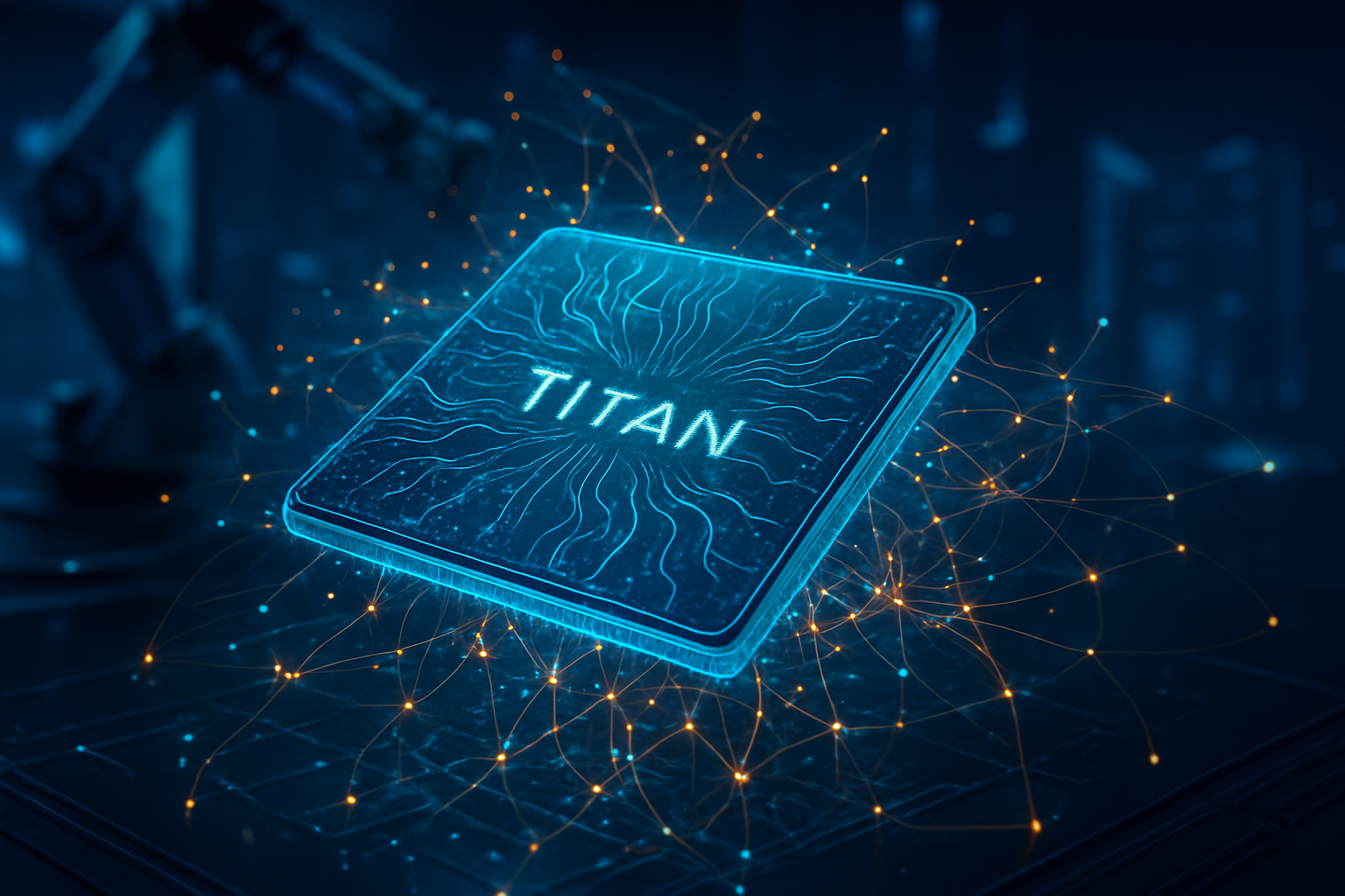
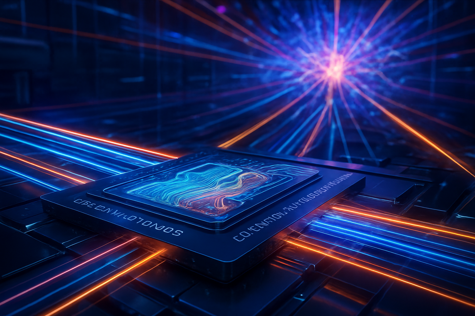
    As of January 2026, the artificial intelligence industry has officially entered what architects are calling the "Era of Light." For years, the rapid advancement of Large Language Models (LLMs) was threatened by two looming physical barriers: the "memory wall"—the bottleneck where data cannot move fast enough between processors and memory—and the "copper wall," where traditional electrical wiring began to fail under the sheer volume of data required for trillion-parameter models. This week, a series of breakthroughs in Silicon Photonics (SiPh) and Optical I/O (Input/Output) have signaled the end of these constraints, effectively decoupling the physical location of hardware from its computational performance.

    The shift is represented most poignantly by the mass commercialization of Co-Packaged Optics (CPO) and optical memory pooling. By replacing copper wires with laser-driven light signals directly on the chip package, industry giants have managed to reduce interconnect power consumption by over 70% while simultaneously increasing bandwidth density by a factor of ten. This transition is not merely an incremental upgrade; it is a fundamental architectural reset that allows data centers to operate as a single, massive "planet-scale" computer rather than a collection of isolated server racks.

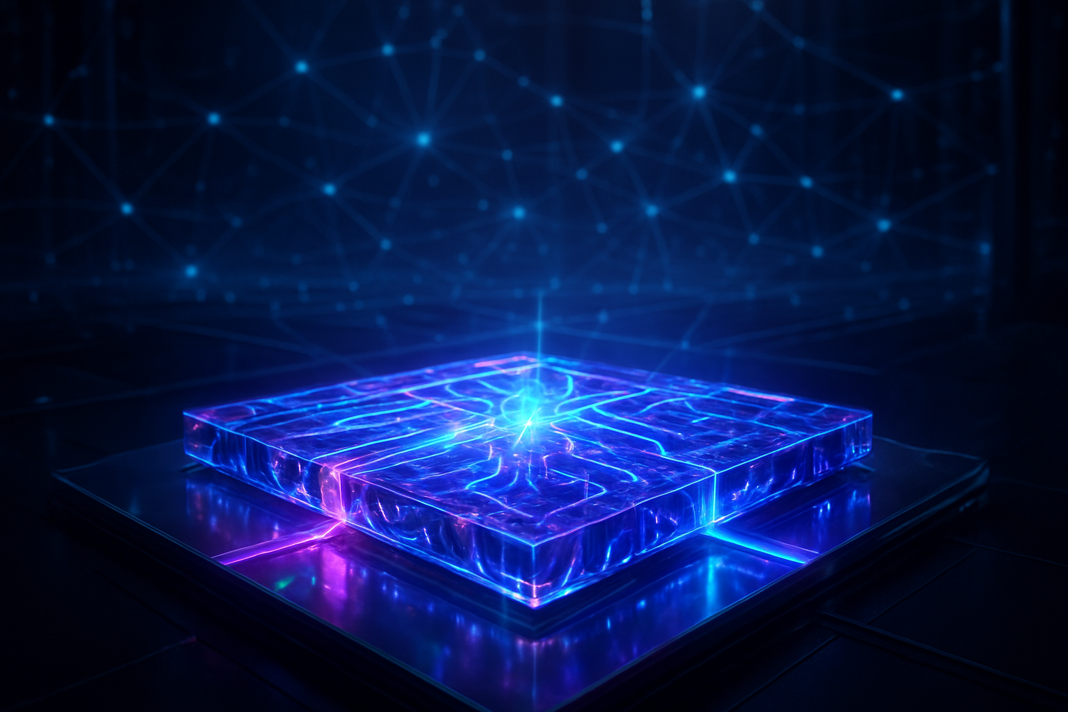
    The Technical Breakdown: Moving Beyond Electrons

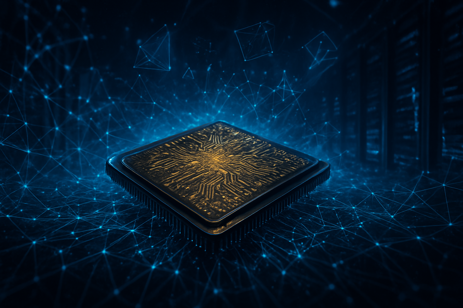
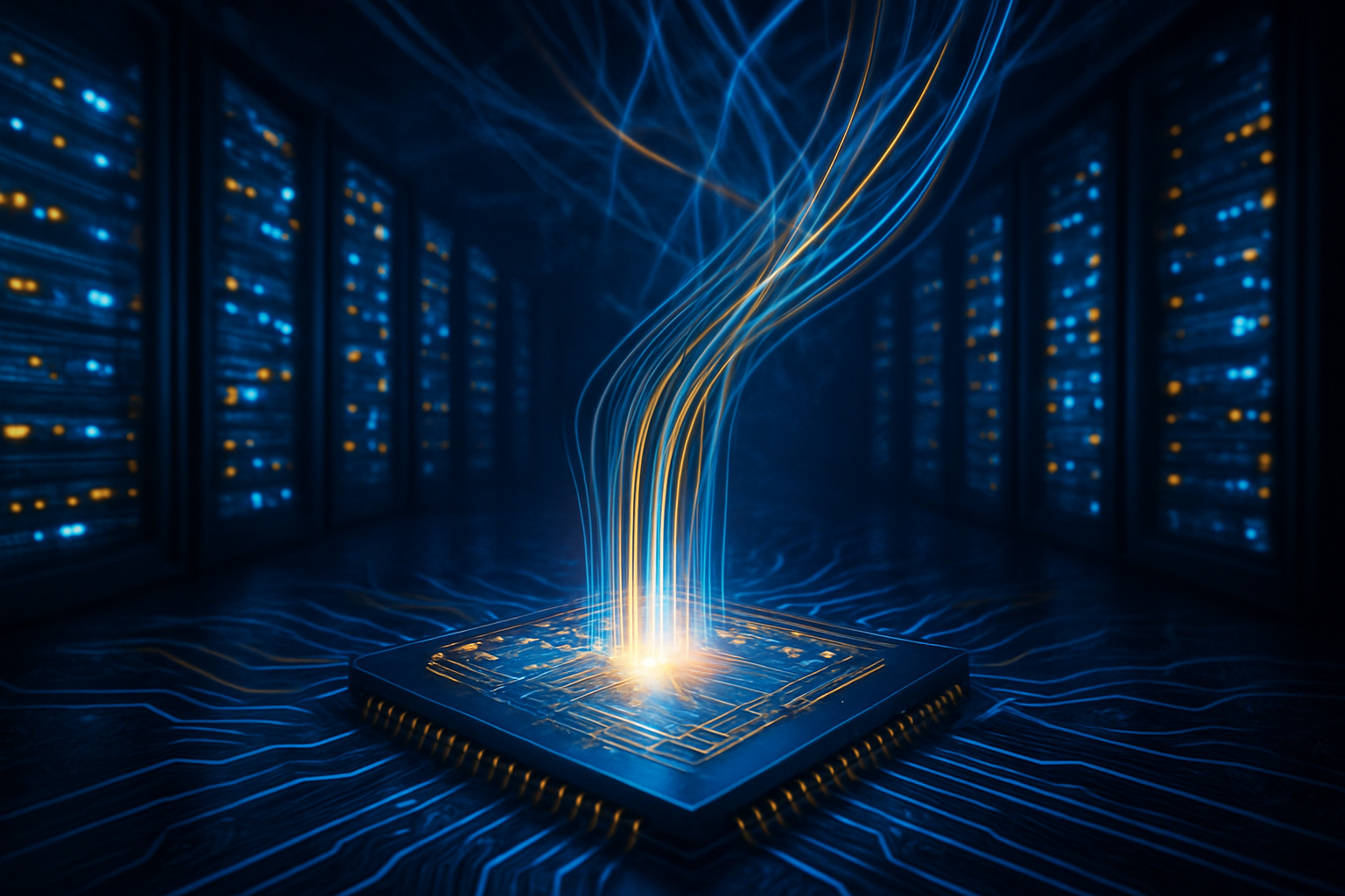
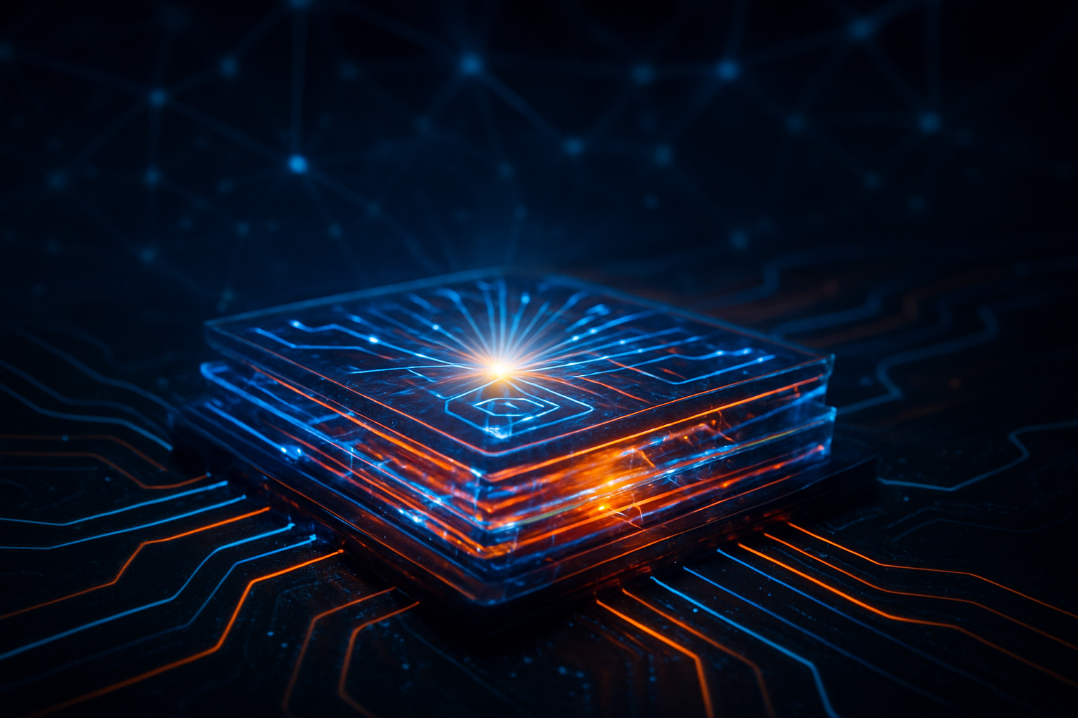
    The core of this advancement lies in the transition from pluggable optics to integrated optical engines. In the previous era, data was moved via copper traces on a circuit board to an optical transceiver at the edge of the rack. At the current 224 Gbps signaling speeds, copper loses its integrity after less than a meter, and the heat generated by electrical resistance becomes unmanageable. The latest technical specifications for January 2026 show that Optical I/O, pioneered by firms like Ayar Labs and Celestial AI (recently acquired by Marvell (NASDAQ: MRVL)), has achieved energy efficiencies of 2.4 to 5 picojoules per bit (pJ/bit), a staggering improvement over the 12–15 pJ/bit required by 2024-era copper systems.

    Central to this breakthrough is the "Optical Compute Interconnect" (OCI) chiplet. Intel (NASDAQ: INTC) has begun high-volume manufacturing of these chiplets using its new glass substrate technology in Arizona. These glass substrates provide the thermal and physical stability necessary to bond photonic engines directly to high-power AI accelerators. Unlike previous approaches that relied on external lasers, these new systems feature "multi-wavelength" light sources that can carry terabits of data across a single fiber-optic strand with latencies below 10 nanoseconds.

    Initial reactions from the AI research community have been electric. Dr. Arati Prabhakar, leading a consortium of high-performance computing (HPC) experts, noted that the move to optical fabrics has "effectively dissolved the physical boundaries of the server." By achieving sub-300ns latency for cross-rack communication, researchers can now train models with tens of trillions of parameters across "million-GPU" clusters without the catastrophic performance degradation that previously plagued large-scale distributed training.

    The Market Landscape: A New Hierarchy of Power

    This shift has created clear winners and losers in the semiconductor space. NVIDIA (NASDAQ: NVDA) has solidified its dominance with the unveiling of the Vera Rubin platform. The Rubin architecture utilizes NVLink 6 and the Spectrum-6 Ethernet switch, the latter of which is the world’s first to fully integrate Spectrum-X Ethernet Photonics. By moving to an all-optical backplane, NVIDIA has managed to double GPU-to-GPU bandwidth to 3.6 TB/s while significantly lowering the total cost of ownership for cloud providers by slashing cooling requirements.

    Broadcom (NASDAQ: AVGO) remains the titan of the networking layer, now shipping its Tomahawk 6 "Davisson" switch in massive volumes. This 102.4 Tbps switch utilizes TSMC (NYSE: TSM) "COUPE" (Compact Universal Photonic Engine) technology, which heterogeneously integrates optical engines and silicon into a single 3D package. This integration has forced traditional networking companies like Cisco (NASDAQ: CSCO) to pivot aggressively toward silicon-proven optical solutions to avoid being marginalized in the AI-native data center.

    The strategic advantage now belongs to those who control the "Scale-Up" fabric—the interconnects that allow thousands of GPUs to work as one. Marvell’s (NASDAQ: MRVL) acquisition of Celestial AI has positioned them as the primary provider of optical memory appliances. These devices provide up to 33TB of shared HBM4 capacity, allowing any GPU in a data center to access a massive pool of memory as if it were on its own local bus. This "disaggregated" approach is a nightmare for legacy server manufacturers but a boon for hyperscalers like Amazon and Google, who are desperate to maximize the utilization of their expensive silicon.

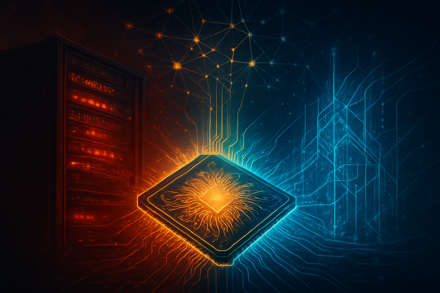
    Wider Significance: Environmental and Architectural Rebirth

    The rise of Silicon Photonics is about more than just speed; it is the industry’s most viable answer to the environmental crisis of AI energy consumption. Data centers were on a trajectory to consume an unsustainable percentage of global electricity by 2030. However, the 70% reduction in interconnect power offered by optical I/O provides a necessary "reset" for the industry’s carbon footprint. By moving data with light instead of heat-generating electrons, the energy required for data movement—which once accounted for 30% of a cluster’s power—has been drastically curtailed.

    Historically, this milestone is being compared to the transition from vacuum tubes to transistors. Just as the transistor allowed for a scale of complexity that was previously impossible, Silicon Photonics allows for a scale of data movement that finally matches the computational potential of modern neural networks. The "Memory Wall," a term coined in the mid-1990s, has been the single greatest hurdle in computer architecture for thirty years. To see it finally "shattered" by light-based memory pooling is a moment that will likely define the next decade of computing history.

    However, concerns remain regarding the "Yield Wars." The 3D stacking of silicon, lasers, and optical fibers is incredibly complex. As TSMC, Samsung (KOSPI: 005930), and Intel compete for dominance in these advanced packaging techniques, any slip in manufacturing yields could cause massive supply chain disruptions for the world's most critical AI infrastructure.

    The Road Ahead: Planet-Scale Compute and Beyond

    In the near term, we expect to see the "Optical-to-the-XPU" movement accelerate. Within the next 18 to 24 months, we anticipate the release of AI chips that have no electrical I/O whatsoever, relying entirely on fiber optic connections for both power delivery and data. This will enable "cold racks," where high-density compute can be submerged in dielectric fluid or specialized cooling environments without the interference caused by traditional copper cabling.

    Long-term, the implications for AI applications are profound. With the memory wall removed, we are likely to see a surge in "long-context" AI models that can process entire libraries of data in their active memory. Use cases in drug discovery, climate modeling, and real-time global economic simulation—which require massive, shared datasets—will become feasible for the first time. The challenge now shifts from moving the data to managing the sheer scale of information that can be accessed at light speed.

    Experts predict that the next major hurdle will be "Optical Computing" itself—using light not just to move data, but to perform the actual matrix multiplications required for AI. While still in the early research phases, the success of Silicon Photonics in I/O has proven that the industry is ready to embrace photonics as the primary medium of the information age.

    Conclusion: The Light at the End of the Tunnel

    The emergence of Silicon Photonics and Optical I/O represents a landmark achievement in the history of technology. By overcoming the twin barriers of the memory wall and the copper wall, the semiconductor industry has cleared the path for the next generation of artificial intelligence. Key takeaways include the dramatic shift toward energy-efficient, high-bandwidth optical fabrics and the rise of memory pooling as a standard for AI infrastructure.

    As we look toward the coming weeks and months, the focus will shift from these high-level announcements to the grueling reality of manufacturing scale. Investors and engineers alike should watch the quarterly yield reports from major foundries and the deployment rates of the first "Vera Rubin" clusters. The era of the "Copper Data Center" is ending, and in its place, a faster, cooler, and more capable future is being built on a foundation of light.


    This content is intended for informational purposes only and represents analysis of current AI developments.

    TokenRing AI delivers enterprise-grade solutions for multi-agent AI workflow orchestration, AI-powered development tools, and seamless remote collaboration platforms.
    For more information, visit https://www.tokenring.ai/.

  • The Speed of Light: Silicon Photonics and CPO Emerge as the Backbone of the ‘Million-GPU’ AI Power Grid

    The Speed of Light: Silicon Photonics and CPO Emerge as the Backbone of the ‘Million-GPU’ AI Power Grid

    As of January 2026, the artificial intelligence industry has reached a pivotal physical threshold. For years, the scaling of large language models was limited by compute density and memory capacity. Today, however, the primary bottleneck has shifted to the "Energy Wall"—the staggering amount of power required simply to move data between processors. To shatter this barrier, the semiconductor industry is undergoing its most significant architectural shift in a decade: the transition from copper-based electrical signaling to light-based interconnects. Silicon Photonics and Co-Packaged Optics (CPO) are no longer experimental concepts; they have become the critical infrastructure, or the "backbone," of the modern AI power grid.

    The significance of this transition cannot be overstated. As hyperscalers race toward building "million-GPU" clusters to train the next generation of Artificial General Intelligence (AGI), the traditional "I/O tax"—the energy consumed by data moving across a data center—has threatened to stall progress. By integrating optical engines directly onto the chip package, companies are now able to reduce data-transfer energy consumption by up to 70%, effectively redirecting megawatts of power back into actual computation. This month marks a major milestone in this journey, as the industry’s biggest players, including TSMC (NYSE: TSM), Broadcom (NASDAQ: AVGO), and Ayar Labs, unveil the production-ready hardware that will define the AI landscape for the next five years.

    Breaking the Copper Wall: Technical Foundations of 2026

    The technical heart of this revolution lies in the move from pluggable transceivers to Co-Packaged Optics. Leading the charge is Taiwan Semiconductor Manufacturing Company (TPE: 2330), whose Compact Universal Photonic Engine (COUPE) technology has entered its final production validation phase this January, with full-scale mass production slated for the second half of 2026. COUPE utilizes TSMC’s proprietary SoIC-X (System on Integrated Chips) 3D-stacking technology to place an Electronic Integrated Circuit (EIC) directly on top of a Photonic Integrated Circuit (PIC). This configuration eliminates the parasitic capacitance of traditional wiring, supporting staggering bandwidths of 1.6 Tbps in its first generation, with a roadmap toward 12.8 Tbps by 2028.

    Simultaneously, Broadcom (NASDAQ: AVGO) has begun shipping pilot units of its Gen 3 CPO platform, powered by the Tomahawk 6 (code-named "Davisson") switch silicon. This generation introduces 200 Gbps per lane optical connectivity, enabling the construction of 102.4 Tbps Ethernet switches. Unlike previous iterations, Broadcom’s Gen 3 removes the power-hungry Digital Signal Processor (DSP) from the optical module, utilizing a "direct drive" architecture that slashes latency to under 10 nanoseconds. This is critical for the "scale-up" fabrics required by NVIDIA (NASDAQ: NVDA) and AMD (NASDAQ: AMD), where thousands of GPUs must act as a single, massive processor without the lag inherent in traditional networking.

    Further diversifying the ecosystem is the partnership between Ayar Labs and Global Unichip Corp (TPE: 3443). The duo has successfully integrated Ayar Labs’ TeraPHY™ optical engines into GUC’s advanced ASIC design workflow. Using the Universal Chiplet Interconnect Express (UCIe) standard, they have achieved a "shoreline density" of 1.4 Tbps/mm², allowing more than 100 Tbps of aggregate bandwidth from a single processor package. This approach solves the mechanical and thermal challenges of CPO by using specialized "stiffener" designs and detachable fiber connectors, making light-based I/O accessible for custom AI accelerators beyond just the major GPU vendors.

    A New Competitive Frontier for Hyperscalers and Chipmakers

    The shift to silicon photonics creates a clear divide between those who can master light-based interconnects and those who cannot. For major AI labs and hyperscalers like Google (NASDAQ: GOOGL) and Meta (NASDAQ: META), this technology is the "buy" that allows them to scale their data centers from single buildings to entire "AI Factories." By reducing the "I/O tax" from 20 picojoules per bit (pJ/bit) to less than 5 pJ/bit, these companies can operate much larger clusters within the same power envelope, providing a massive strategic advantage in the race for AGI.

    NVIDIA and AMD are the most immediate beneficiaries. NVIDIA is already preparing its "Rubin Ultra" platform to integrate TSMC’s COUPE technology, ensuring its leadership in the "scale-up" domain where low-latency communication is king. Meanwhile, Broadcom’s dominance in the networking fabric allows it to act as the primary "toll booth" for the AI power grid. For startups, the Ayar Labs and GUC partnership is a game-changer; it provides a standardized, validated path to integrate optical I/O into bespoke AI silicon, potentially disrupting the dominance of off-the-shelf GPUs by allowing specialized chips to communicate at speeds previously reserved for top-tier hardware.

    However, this transition is not without risk. The move to CPO disrupts the traditional "pluggable" optics market, long dominated by specialized module makers. As optical engines move onto the chip package, the traditional supply chain is being compressed, forcing many optics companies to either partner with foundries or face obsolescence. The market positioning of TSMC as a "one-stop shop" for both logic and photonics packaging further consolidates power in the hands of the world's largest foundry, raising questions about future supply chain resilience.

    Lighting the Way to AGI: Wider Significance

    The rise of silicon photonics represents more than just a faster way to move data; it is a fundamental shift in the AI landscape. In the era of the "Copper Wall," physical distance was a dealbreaker—high-speed electrical signals could only travel about a meter before degrading. This limited AI clusters to single racks or small rows. Silicon photonics extends that reach to over 100 meters without significant signal loss. This enables the "million-GPU" vision where a "scale-up" domain can span an entire data hall, allowing models to be trained on datasets and at scales that were previously physically impossible.

    Comparatively, this milestone is as significant as the transition from HDD to SSD or the move to FinFET transistors. It addresses the sustainability crisis currently facing the tech industry. As data centers consume an ever-increasing percentage of global electricity, the 70% energy reduction offered by CPO is a critical "green" technology. Without it, the environmental and economic cost of training models like GPT-6 or its successors would likely have become prohibitive, potentially triggering an "AI winter" driven by resource constraints rather than lack of algorithmic progress.

    However, concerns remain regarding the reliability of laser sources. Unlike electronic components, lasers have a finite lifespan and are sensitive to the high heat generated by AI processors. The industry is currently split between "internal" lasers integrated into the package and "External Laser Sources" (ELS) that can be swapped out like a lightbulb. How the industry settles this debate in 2026 will determine the long-term maintainability of the world's most expensive compute clusters.

    The Horizon: From 1.6T to 12.8T and Beyond

    Looking ahead to the remainder of 2026 and into 2027, the focus will shift from "can we do it" to "can we scale it." Following the H2 2026 mass production of first-gen COUPE, experts predict an immediate push toward the 6.4 Tbps generation. This will likely involve even tighter integration with CoWoS (Chip-on-Wafer-on-Substrate) packaging, effectively blurring the line between the processor and the network. We expect to see the first "All-Optical" AI data center prototypes emerge by late 2026, where even the memory-to-processor links utilize silicon photonics.

    Near-term developments will also focus on the standardization of the "optical chiplet." With UCIe-S and UCIe-A standards gaining traction, we may see a marketplace where companies can mix and match logic chiplets from one vendor with optical chiplets from another. The ultimate goal is "Optical I/O for everything," extending from the high-end GPU down to consumer-grade AI PCs and edge devices, though those applications remain several years away. Challenges like fiber-attach automation and high-volume testing of photonic circuits must be addressed to bring costs down to the level of traditional copper.

    Summary and Final Thoughts

    The emergence of Silicon Photonics and Co-Packaged Optics as the backbone of the AI power grid marks the end of the "Copper Age" of computing. By leveraging the speed and efficiency of light, TSMC, Broadcom, Ayar Labs, and their partners have provided the industry with a way over the "Energy Wall." With TSMC’s COUPE entering mass production in H2 2026 and Broadcom’s Gen 3 CPO already in the hands of hyperscalers, the infrastructure for the next generation of AI is being laid today.

    In the history of AI, this will likely be remembered as the moment when physical hardware caught up to the ambitions of software. The transition to light-based interconnects ensures that the scaling laws which have driven AI progress so far can continue for at least another decade. In the coming weeks and months, all eyes will be on the first deployment data from Broadcom’s Tomahawk 6 pilots and the final yield reports from TSMC’s COUPE validation lines. The era of the "Million-GPU" cluster has officially begun, and it is powered by light.


    This content is intended for informational purposes only and represents analysis of current AI developments.

    TokenRing AI delivers enterprise-grade solutions for multi-agent AI workflow orchestration, AI-powered development tools, and seamless remote collaboration platforms.
    For more information, visit https://www.tokenring.ai/.

  • OpenAI Signals End of the ‘Nvidia Tax’ with 2026 Launch of Custom ‘Titan’ Chip

    OpenAI Signals End of the ‘Nvidia Tax’ with 2026 Launch of Custom ‘Titan’ Chip

    In a decisive move toward vertical integration, OpenAI has officially unveiled the roadmap for its first custom-designed AI processor, codenamed "Titan." Developed in close collaboration with Broadcom (NASDAQ: AVGO) and slated for fabrication on Taiwan Semiconductor Manufacturing Company's (NYSE: TSM) cutting-edge N3 process, the chip represents a fundamental shift in OpenAI’s strategy. By moving from a software-centric model to a "fabless" semiconductor designer, the company aims to break its reliance on general-purpose hardware and gain direct control over the infrastructure powering its next generation of reasoning models.

    The announcement marks the formal pivot away from CEO Sam Altman's ambitious earlier discussions regarding a multi-trillion-dollar global foundry network. Instead, OpenAI is adopting what industry insiders call the "Apple Playbook," focusing on proprietary Application-Specific Integrated Circuit (ASIC) design to optimize performance-per-watt and, more critically, performance-per-dollar. With a target deployment date of December 2026, the Titan chip is engineered specifically to tackle the skyrocketing costs of inference—the phase where AI models generate responses—which have threatened to outpace the company’s revenue growth as models like the o1-series become more "thought-intensive."

    Technical Specifications: Optimizing for the Reasoning Era

    The Titan chip is not a general-purpose GPU meant to compete with Nvidia (NASDAQ: NVDA) across every possible workload; rather, it is a specialized ASIC fine-tuned for the unique architectural demands of Large Language Models (LLMs) and reasoning-heavy agents. Built on TSMC's 3-nanometer (N3) node, the Titan project leverages Broadcom's extensive library of intellectual property, including high-speed interconnects and sophisticated Ethernet switching. This collaboration is designed to create a "system-on-a-chip" environment that minimizes the latency between the processor and its high-bandwidth memory (HBM), a critical bottleneck in modern AI systems.

    Initial technical leaks suggest that Titan aims for a staggering 90% reduction in inference costs compared to existing general-purpose hardware. This is achieved by stripping away the legacy features required for graphics or scientific simulations—functions found in Nvidia’s Blackwell or Vera Rubin architectures—and focusing entirely on the "thinking cycles" required for autoregressive token generation. By optimizing the hardware specifically for OpenAI’s proprietary algorithms, Titan is expected to handle the "chain-of-thought" processing of future models with far greater energy efficiency than traditional GPUs.

    The AI research community has reacted with a mix of awe and skepticism. While many experts agree that custom silicon is the only way to scale inference to billions of users, others point out the risks of "architectural ossification." Because ASICs are hard-wired for specific tasks, a sudden shift in AI model architecture (such as a move away from Transformers) could render the Titan chip obsolete before it even reaches full scale. However, OpenAI’s decision to continue deploying Nvidia’s hardware alongside Titan suggests a "hybrid" strategy intended to mitigate this risk while lowering the baseline cost for their most stable workloads.

    Market Disruption: The Rise of the Hyperscaler Silicon

    The entry of OpenAI into the silicon market sends a clear message to the broader tech industry: the era of the "Nvidia tax" is nearing its end for the world’s largest AI labs. OpenAI joins an elite group of tech giants, including Google (NASDAQ: GOOGL) with its TPU v7 and Amazon (NASDAQ: AMZN) with its Trainium line, that are successfully decoupling their futures from third-party hardware vendors. This vertical integration allows these companies to capture the margins previously paid to semiconductor giants and gives them a strategic advantage in a market where compute capacity is the most valuable currency.

    For companies like Meta (NASDAQ: META), which is currently ramping up its own Meta Training and Inference Accelerator (MTIA), the Titan project serves as both a blueprint and a warning. The competitive landscape is shifting from "who has the best model" to "who can run the best model most cheaply." If OpenAI successfully hits its December 2026 deployment target, it could offer its API services at a price point that undercuts competitors who remain tethered to general-purpose GPUs. This puts immense pressure on mid-sized AI startups who lack the capital to design their own silicon, potentially widening the gap between the "compute-rich" and the "compute-poor."

    Broadcom stands as a major beneficiary of this shift. Despite a slight market correction in early 2026 due to lower initial margins on custom ASICs, the company has secured a massive $73 billion AI backlog. By positioning itself as the "architect for hire" for OpenAI and others, Broadcom has effectively cornered a new segment of the market: the custom AI silicon designer. Meanwhile, TSMC continues to act as the industry's ultimate gatekeeper, with its 3nm and 5nm nodes reportedly 100% booked through the end of 2026, forcing even the world’s most powerful companies to wait in line for manufacturing capacity.

    The Broader AI Landscape: From Foundries to Infrastructure

    The Titan project is the clearest indicator yet that the "trillions for foundries" narrative has evolved into a more pragmatic pursuit of "industrial infrastructure." Rather than trying to rebuild the global semiconductor supply chain from scratch, OpenAI is focusing its capital on what it calls the "Stargate" project—a $500 billion collaboration with Microsoft (NASDAQ: MSFT) and Oracle (NYSE: ORCL) to build massive data centers. Titan is the heart of this initiative, designed to fill these facilities with processors that are more efficient and less power-hungry than anything currently on the market.

    This development also highlights the escalating energy crisis within the AI sector. With OpenAI targeting a total compute commitment of 26 gigawatts, the efficiency of the Titan chip is not just a financial necessity but an environmental and logistical one. As power grids around the world struggle to keep up with the demands of AI, the ability to squeeze more "intelligence" out of every watt of electricity will become the primary metric of success. Comparisons are already being drawn to the early days of mobile computing, where proprietary silicon allowed companies like Apple to achieve battery life and performance levels that generic competitors could not match.

    However, the concentration of power remains a significant concern. By controlling the model, the software, and now the silicon, OpenAI is creating a closed ecosystem that could stifle open-source competition. If the most efficient way to run advanced AI is on proprietary hardware that is not for sale to the public, the "democratization of AI" may face its greatest challenge yet. The industry is watching closely to see if OpenAI will eventually license the Titan architecture or keep it strictly for internal use, further cementing its position as a sovereign entity in the tech world.

    Looking Ahead: The Roadmap to Titan 2 and Beyond

    The December 2026 launch of the first Titan chip is only the beginning. Sources indicate that OpenAI is already deep into the design phase for "Titan 2," which is expected to utilize TSMC’s A16 (1.6nm) process by 2027. This rapid iteration cycle suggests that OpenAI intends to match the pace of the semiconductor industry, releasing new hardware generations as frequently as it releases new model versions. Near-term, the focus will remain on stabilizing the N3 production yields and ensuring that the first racks of Titan servers are fully integrated into OpenAI’s existing data center clusters.

    In the long term, the success of Titan could pave the way for even more specialized hardware. We may see the emergence of "edge" versions of the Titan chip, designed to bring high-level reasoning capabilities to local devices without relying on the cloud. Challenges remain, particularly in the realm of global logistics and the ongoing geopolitical tensions surrounding semiconductor manufacturing in Taiwan. Any disruption to TSMC’s operations would be catastrophic for the Titan timeline, making supply chain resilience a top priority for Altman’s team as they move toward the late 2026 deadline.

    Experts predict that the next eighteen months will be a "hardware arms race" unlike anything seen since the early days of the PC. As OpenAI transitions from a software company to a hardware-integrated powerhouse, the boundary between "AI company" and "semiconductor company" will continue to blur. If Titan performs as promised, it will not only secure OpenAI’s financial future but also redefine the physical limits of what artificial intelligence can achieve.

    Conclusion: A New Chapter in AI History

    OpenAI's entry into the custom silicon market with the Titan chip marks a historic turning point. It is a calculated bet that the future of artificial intelligence belongs to those who own the entire stack, from the silicon atoms to the neural networks. By partnering with Broadcom and TSMC, OpenAI has bypassed the impossible task of building its own factories while still securing a customized hardware advantage that could last for years.

    The key takeaway for 2026 is that the AI industry has reached industrial maturity. No longer content with off-the-shelf solutions, the leaders of the field are now building the world they want to see, one transistor at a time. While the technical and geopolitical risks are substantial, the potential reward—a 90% reduction in the cost of intelligence—is too great to ignore. In the coming months, all eyes will be on TSMC’s fabrication schedules and the internal benchmarks of the first Titan prototypes, as the world waits to see if OpenAI can truly conquer the physical layer of the AI revolution.


    This content is intended for informational purposes only and represents analysis of current AI developments.

    TokenRing AI delivers enterprise-grade solutions for multi-agent AI workflow orchestration, AI-powered development tools, and seamless remote collaboration platforms.
    For more information, visit https://www.tokenring.ai/.

  • The Silicon Sovereignty: How Hyperscalers are Rewiring the AI Economy with Custom Chips

    The Silicon Sovereignty: How Hyperscalers are Rewiring the AI Economy with Custom Chips

    The era of the general-purpose AI chip is facing its first major existential challenge. As of January 2026, the world’s largest technology companies—Google, Microsoft, Meta, and Amazon—have moved beyond the "experimental" phase of hardware development, aggressively deploying custom-designed AI silicon to power the next generation of generative models and agentic services. This strategic pivot marks a fundamental shift in the AI supply chain, as hyperscalers attempt to break their near-total dependence on third-party hardware providers while tailoring chips to the specific mathematical demands of their proprietary software stacks.

    The immediate significance of this shift cannot be overstated. By moving high-volume workloads like inference and recommendation ranking to in-house Application-Specific Integrated Circuits (ASICs), these tech giants are significantly reducing their Total Cost of Ownership (TCO) and power consumption. While NVIDIA (NASDAQ: NVDA) remains the gold standard for frontier model training, the rise of specialized silicon from the likes of Alphabet (NASDAQ: GOOGL), Microsoft (NASDAQ: MSFT), Meta Platforms (NASDAQ: META), and Amazon (NASDAQ: AMZN) is creating a tiered hardware ecosystem where bespoke chips handle the "workhorse" tasks of the digital economy.

    The Technical Vanguard: TPU v7, Maia 200, and the 3nm Frontier

    At the forefront of this technical evolution is Google’s TPU v7 (Ironwood), which entered general availability in late 2025. Built on a cutting-edge 3nm process, the TPU v7 utilizes a dual-chiplet architecture specifically optimized for the Mixture of Experts (MoE) models that power the Gemini ecosystem. With compute performance reaching approximately 4.6 PFLOPS in FP8 dense math, the Ironwood chip is the first custom ASIC to achieve parity with Nvidia’s Blackwell architecture in raw throughput. Crucially, Google’s 3D torus interconnect technology allows for the seamless scaling of up to 9,216 chips in a single pod, creating a multi-exaflop environment that rivals the most advanced commercial clusters.

    Meanwhile, Microsoft has finally brought its Maia 200 (Braga) into mass production after a series of design revisions aimed at meeting the extreme requirements of OpenAI. Unlike Google’s broad-spectrum approach, the Maia 200 is a "precision instrument," focusing on high-speed tensor units and a specialized "Microscaling" (MX) data format designed to slash power consumption during massive inference runs for Azure OpenAI and Copilot. Similarly, Amazon Web Services (AWS) has unified its hardware roadmap with Trainium 3, its first 3nm chip. Trainium 3 has shifted from a niche training accelerator to a high-density compute engine, boasting 2.52 PFLOPS of FP8 performance and serving as the backbone for partners like Anthropic.

    Meta’s MTIA v3 represents a different philosophical approach. Rather than chasing peak FLOPs for training the world’s largest models, Meta has focused on the "Inference Tax"—the massive cost of running real-time recommendations for billions of users. The MTIA v3 prioritizes TOPS per Watt (efficiency) over raw power, utilizing a chiplet-based design that reportedly beats Nvidia's previous-generation H100 in energy efficiency by nearly 40%. This efficiency is critical for Meta’s pivot toward "Agentic AI," where thousands of small, specialized models must run simultaneously to power proactive digital assistants.

    The Kingmakers: Broadcom, Marvell, and the Designer Shift

    While the hyperscalers are the public faces of this silicon revolution, the real financial windfall is being captured by the specialized design firms that make these chips possible. Broadcom (NASDAQ: AVGO) has emerged as the undisputed "King of ASICs," securing its position as the primary co-design partner for Google, Meta, and reportedly, future iterations of Microsoft’s hardware. Broadcom’s role has evolved from providing simple networking IP to managing the entire physical design flow and high-speed interconnects (SerDes) necessary for 3nm production. Analysts project that Broadcom’s AI-related revenue will exceed $40 billion in fiscal 2026, driven almost entirely by these hyperscaler partnerships.

    Marvell Technology (NASDAQ: MRVL) occupies a more specialized, yet strategic, niche in this new landscape. Although Marvell faced a setback in early 2026 after losing a major contract with AWS to the Taiwanese firm Alchip, it remains a critical player in the AI networking space. Marvell’s focus has shifted toward optical Digital Signal Processors (DSPs) and custom Ethernet switches that allow thousands of custom chips to communicate with minimal latency. Marvell continues to support the "back-end" infrastructure for Meta and Microsoft, positioning itself as the "connective tissue" of the AI data center even as the primary compute dies move to different designers.

    This shift in design partnerships reveals a maturing market where hyperscalers are willing to swap vendors to achieve better yield or faster time-to-market. The competitive landscape is no longer just about who has the fastest chip, but who can deliver the most reliable 3nm design at scale. This has created a high-stakes environment where the "picks and shovels" providers—the design houses and the foundries like TSMC (NYSE: TSM)—hold as much leverage as the platform owners themselves.

    The Broader Landscape: TCO, Energy, and the End of Scarcity

    The transition to custom silicon fits into a larger trend of vertical integration within the tech industry. For years, the AI sector was defined by "GPU scarcity," where the speed of innovation was dictated by Nvidia’s supply chain. By January 2026, that scarcity has largely evaporated, replaced by a focus on "Economics and Electrons." Custom chips like the TPU v7 and Trainium 3 allow hyperscalers to bypass the high margins of third-party vendors, reducing the cost of an AI query by as much as 50% compared to general-purpose hardware.

    However, this silicon sovereignty comes with potential concerns. The fragmentation of the hardware landscape could lead to "vendor lock-in," where models optimized for Google’s TPUs cannot be easily migrated to Azure’s Maia or AWS’s Trainium. While software layers like Triton and various abstraction APIs are attempting to mitigate this, the deep architectural differences—such as the specific memory handling in the Ironwood chips—create natural moats for each cloud provider.

    Furthermore, the move to custom silicon is an environmental necessity. As AI data centers begin to consume a double-digit percentage of the world’s electricity, the efficiency gains provided by ASICs are the only way to sustain the current trajectory of model growth. The "efficiency first" philosophy seen in Meta’s MTIA v3 is likely to become the industry standard, as power availability, rather than chip supply, becomes the primary bottleneck for AI expansion.

    Future Horizons: 2nm, Liquid Cooling, and Chiplet Ecosystems

    Looking toward the late 2020s, the next frontier for custom AI silicon will be the transition to the 2nm process node and the widespread adoption of "System-in-Package" (SiP) designs. Experts predict that by 2027, the distinction between a "chip" and a "server" will continue to blur, as hyperscalers move toward liquid-cooled, rack-scale compute units where the interconnect is integrated directly into the silicon substrate.

    We are also likely to see the rise of "modular" AI silicon. Rather than designing a single monolithic chip, companies may begin to mix and match "chiplets" from different vendors—using a Broadcom compute die with a Marvell networking tile and a third-party memory controller—all tied together with universal interconnect standards. This would allow hyperscalers to iterate even faster, swapping out individual components as new breakthroughs in AI architecture (such as post-transformer models) emerge.

    The primary challenge moving forward will be the "Inference Tax" at the edge. While current custom silicon efforts are focused on massive data centers, the next battleground will be local custom silicon for smartphones and PCs. Apple and Qualcomm have already laid the groundwork, but as Google and Meta look to bring their agentic AI experiences to local devices, the custom silicon war will likely move from the cloud to the pocket.

    A New Era of Computing History

    The aggressive rollout of the TPU v7, Maia 200, and MTIA v3 marks the definitive end of the "one-size-fits-all" era of AI computing. In the history of technology, this shift mirrors the transition from general-purpose CPUs to GPUs decades ago, but at an accelerated pace and with far higher stakes. By seizing control of their own silicon roadmaps, the world's tech giants are not just seeking to lower costs; they are building the physical foundations of a future where AI is woven into every transaction and interaction.

    For the industry, the key takeaways are clear: vertical integration is the new gold standard, and the partnership between hyperscalers and specialist design firms like Broadcom has become the most powerful engine in the global economy. While NVIDIA will likely maintain its lead in the highest-end training applications for the foreseeable future, the "middle market" of AI—where the vast majority of daily compute occurs—is rapidly becoming the domain of the custom ASIC.

    In the coming weeks and months, the focus will shift to how these chips perform in real-world "agentic" workloads. As the first wave of truly autonomous AI agents begins to deploy across enterprise platforms, the underlying silicon will be the ultimate arbiter of which companies can provide the most capable, cost-effective, and energy-efficient intelligence.


    This content is intended for informational purposes only and represents analysis of current AI developments.

    TokenRing AI delivers enterprise-grade solutions for multi-agent AI workflow orchestration, AI-powered development tools, and seamless remote collaboration platforms.
    For more information, visit https://www.tokenring.ai/.

  • The End of the Copper Era: Broadcom and Marvell Usher in the Age of Co-Packaged Optics for AI Supercomputing

    The End of the Copper Era: Broadcom and Marvell Usher in the Age of Co-Packaged Optics for AI Supercomputing

    As artificial intelligence models grow from billions to trillions of parameters, the physical infrastructure supporting them has hit a "power wall." Traditional copper interconnects and pluggable optical modules, which have served as the backbone of data centers for decades, are no longer able to keep pace with the massive bandwidth demands and extreme energy requirements of next-generation AI clusters. In a landmark shift for the industry, semiconductor giants Broadcom Inc. (NASDAQ: AVGO) and Marvell Technology, Inc. (NASDAQ: MRVL) have successfully commercialized Co-Packaged Optics (CPO), a revolutionary technology that integrates light-based communication directly into the heart of the chip.

    This transition marks a pivotal moment in the evolution of data centers. By replacing electrical signals traveling over bulky copper wires with laser-driven light pulses integrated onto the silicon substrate, Broadcom and Marvell are enabling AI clusters to scale far beyond previous physical limits. The move to CPO is not just an incremental speed boost; it is a fundamental architectural redesign that reduces interconnect power consumption by up to 70% and drastically improves the reliability of the massive "back-end" fabrics that link thousands of GPUs and AI accelerators together.

    The Light on the Chip: Breaking the 100-Terabit Barrier

    At the core of this advancement is the integration of Silicon Photonics—the process of manufacturing optical components like lasers, modulators, and detectors using standard CMOS silicon fabrication techniques. Previously, optical communication required separate, "pluggable" modules that sat on the faceplate of a switch. These modules converted electrical signals from the processor into light. However, at speeds of 200G per lane, the electrical signals degrade so rapidly that they require high-power Digital Signal Processors (DSPs) to "clean" the signal before it even reaches the optics. Co-Packaged Optics solves this by placing the optical engine on the same package as the switch ASIC, shortening the electrical path to mere microns and eliminating the need for power-hungry re-timers.

    Broadcom has taken a decisive lead in this space with its third-generation CPO platform, the Tomahawk 6 "Davisson." As of early 2026, the Davisson is the industry’s first 102.4-Tbps switch, utilizing 200G-per-lane optical interfaces integrated via Taiwan Semiconductor Manufacturing Company (NYSE: TSM) and its COUPE (Compact Universal Photonic Engine) technology. This achievement follows the successful field verification of Broadcom’s 51.2T "Bailly" system, which logged over one million cumulative port hours with hyperscalers like Meta Platforms, Inc. (NASDAQ: META). The ability to move 100 terabits of data through a single chip while slashing power consumption is a feat that traditional copper-based architectures simply cannot replicate.

    Marvell has pursued a parallel but specialized strategy, focusing on its "Nova" optical engines and Teralynx switch line. While Broadcom dominates the standard Ethernet switch market, Marvell has pioneered custom CPO solutions for AI accelerators. Their latest "Nova 2" DSPs allow for 1.6-Tbps optical engines that are integrated directly onto the same substrate as the AI processor and High Bandwidth Memory (HBM). This "Optical I/O" approach allows an AI server to communicate across multiple racks with near-zero latency, effectively turning an entire data center into a single, massive GPU. Unlike previous approaches that treated optics as an afterthought, Marvell’s integration makes light an intrinsic part of the compute cycle.

    Realigning the Silicon Power Structure

    The commercialization of CPO is creating a clear divide between the winners and losers of the AI infrastructure boom. Companies like Broadcom and Marvell are solidifying their positions as the indispensable architects of the AI era, moving beyond simple chip design into full-stack interconnect providers. By controlling the optical interface, these companies are capturing value that previously belonged to independent optical module manufacturers. For hyperscale giants like Alphabet Inc. (NASDAQ: GOOGL) and Microsoft Corp. (NASDAQ: MSFT), the shift to CPO is a strategic necessity to manage the soaring electricity costs and thermal management challenges associated with their multi-billion-dollar AI investments.

    The competitive landscape is also shifting for NVIDIA Corp. (NASDAQ: NVDA). While NVIDIA’s proprietary NVLink has long been the gold standard for intra-rack GPU communication, the emergence of CPO-enabled Ethernet is providing a viable, open-standard alternative for "scale-out" and "scale-up" networking. Broadcom’s Scale-Up Ethernet (SUE) framework, powered by CPO, now allows massive clusters of up to 1,024 nodes to communicate with the efficiency of a single machine. This creates a more competitive market where cloud providers are no longer locked into a single vendor's proprietary networking stack, potentially disrupting NVIDIA’s end-to-end dominance in the AI cluster market.

    A Greener, Faster Horizon for Artificial Intelligence

    The wider significance of Co-Packaged Optics extends beyond just speed; it is perhaps the most critical technology for the environmental sustainability of AI. As the world grows concerned over the massive power consumption of AI data centers, CPO offers a rare "free lunch"—higher performance for significantly less energy. By eliminating the "DSP tax" associated with traditional pluggable modules, CPO can save hundreds of megawatts of power across a single large-scale deployment. This energy efficiency is the only way for the industry to reach the 200.0T and 400.0T bandwidth levels expected in the late 2020s without building dedicated power plants for every data center.

    Furthermore, this transition represents a major milestone in the history of computing. Much like the transition from vacuum tubes to transistors, the shift from electrical to optical chip-to-chip communication represents a phase change in how information is processed. We are moving toward a future where "computing" and "networking" are no longer distinct categories. In the CPO era, the network is the computer. This shift mirrors earlier breakthroughs like the introduction of HBM, which solved the "memory wall"; now, CPO is solving the "interconnect wall," ensuring that the rapid progress of AI models is not throttled by the physical limitations of copper.

    The Road to 200T and Beyond

    Looking ahead, the near-term focus will be on the mass deployment of 102.4T CPO systems throughout 2026. Industry experts predict that as these systems become the standard, the focus will shift toward even tighter integration. We are likely to see "Optical Chiplets" where the laser itself is integrated into the silicon, though the current "External Laser" (ELSFP) approach used by Broadcom remains the favorite for its serviceability. By 2027, the industry is expected to begin sampling 204.8T switches, a milestone that would be physically impossible without the density provided by Silicon Photonics.

    The long-term challenge remains the manufacturing yield of these highly complex, heterogeneous packages. Combining high-speed logic, memory, and photonics into a single package is a feat of extreme engineering that requires flawless execution from foundry partners. However, as the ecosystem around the Ultra Accelerator Link (UALink) and other open standards matures, the hurdles of interoperability and multi-vendor support are being cleared. The next major frontier will be bringing optical I/O directly into consumer-grade hardware, though that remains a goal for the end of the decade.

    A Brighter Future for AI Networking

    The successful commercialization of Co-Packaged Optics by Broadcom and Marvell signals the definitive end of the "Copper Era" for high-performance AI networking. By successfully integrating light into the chip package, these companies have provided the essential plumbing needed for the next generation of generative AI and autonomous systems. The significance of this development cannot be overstated: it is the primary technological enabler that allows AI scaling to continue its exponential trajectory while keeping power budgets within the realm of reality.

    In the coming weeks and months, the industry will be watching for the first large-scale performance benchmarks of the TH6-Davisson and Nova 2 systems as they go live in flagship AI clusters. As these results emerge, the shift from pluggable optics to CPO is expected to accelerate, fundamentally changing the hardware profile of the modern data center. For the AI industry, the future is no longer just digital—it is optical.


    This content is intended for informational purposes only and represents analysis of current AI developments.

    TokenRing AI delivers enterprise-grade solutions for multi-agent AI workflow orchestration, AI-powered development tools, and seamless remote collaboration platforms.
    For more information, visit https://www.tokenring.ai/.

  • The DeepSeek Effect: How Ultra-Efficient Models Cracked the Code of Semiconductor “Brute Force”

    The DeepSeek Effect: How Ultra-Efficient Models Cracked the Code of Semiconductor “Brute Force”

    The artificial intelligence industry is currently undergoing its most significant structural shift since the "Attention is All You Need" paper, driven by what analysts have dubbed the "DeepSeek Effect." This phenomenon, sparked by the release of DeepSeek-V3 and the reasoning-optimized DeepSeek-R1 in early 2025, has fundamentally shattered the "brute force" scaling laws that defined the first half of the decade. By demonstrating that frontier-level intelligence could be achieved for a fraction of the traditional training cost—most notably training a GPT-4 class model for approximately $6 million—DeepSeek has forced the world's most powerful semiconductor firms to abandon pure TFLOPS (Teraflops) competition in favor of architectural efficiency.

    As of early 2026, the ripple effects of this development have transformed the stock market and data center construction alike. The industry is no longer engaged in a race to build the largest possible GPU clusters; instead, it is pivoting toward a "sparse computation" paradigm. This shift focuses on silicon that can intelligently route data to only the necessary parts of a model, effectively ending the era of dense models where every transistor in a chip fired for every single token processed. The result is a total re-engineering of the AI stack, from the gate level of transistors to the multi-billion-dollar interconnects of global data centers.

    Breaking the Memory Wall: MoE, MLA, and the End of Dense Compute

    At the heart of the DeepSeek Effect are three core technical innovations that have redefined how hardware is utilized: Mixture-of-Experts (MoE), Multi-Head Latent Attention (MLA), and Multi-Token Prediction (MTP). While MoE has existed for years, DeepSeek-V3 scaled it to an unprecedented 671 billion parameters while ensuring that only 37 billion parameters are active for any given token. This "sparse activation" allows a model to possess the "knowledge" of a massive system while only requiring the "compute" of a much smaller one. For chipmakers, this has shifted the priority from raw matrix-multiplication speed to "routing" efficiency—the ability of a chip to quickly decide which "expert" circuit to activate for a specific input.

    The most profound technical breakthrough, however, is Multi-Head Latent Attention (MLA). Previous frontier models suffered from the "KV Cache bottleneck," where the memory required to maintain a conversation’s context grew linearly, eventually choking even the most advanced GPUs. MLA solves this by compressing the Key-Value cache into a low-dimensional "latent" space, reducing memory overhead by up to 93%. This innovation essentially "broke" the memory wall, allowing chips with lower memory capacity to handle massive context windows that were previously the exclusive domain of $40,000 top-tier accelerators.

    Initial reactions from the AI research community were a mix of shock and strategic realignment. Experts at Stanford and MIT noted that DeepSeek’s success proved algorithmic ingenuity could effectively act as a substitute for massive silicon investments. Industry giants who had bet their entire 2025-2030 roadmaps on "brute force" scaling—the idea that more GPUs and more power would always equal more intelligence—were suddenly forced to justify their multi-billion dollar capital expenditures (CAPEX) in a world where a $6 million training run could match their output.

    The Silicon Pivot: NVIDIA, Broadcom, and the Custom ASIC Surge

    The market implications of this shift were felt most acutely on "DeepSeek Monday" in late January 2025, when NVIDIA (NASDAQ: NVDA) saw a historic $600 billion drop in market value as investors questioned the long-term necessity of massive H100 clusters. Since then, NVIDIA has aggressively pivoted its roadmap. In early 2026, the company accelerated the release of its Rubin architecture, which is the first NVIDIA platform specifically designed for sparse MoE models. Unlike the Blackwell series, Rubin features dedicated "MoE Routers" at the hardware level to minimize the latency of expert switching, signaling that NVIDIA is now an "efficiency-first" company.

    While NVIDIA has adapted, the real winners of the DeepSeek Effect have been the custom silicon designers. Broadcom (NASDAQ: AVGO) and Marvell (NASDAQ: MRVL) have seen a surge in orders as AI labs move away from general-purpose GPUs toward Application-Specific Integrated Circuits (ASICs). In a landmark $21 billion deal revealed this month, Anthropic commissioned nearly one million custom "Ironwood" TPU v7p chips from Broadcom. These chips are reportedly optimized for Anthropic’s new Claude architectures, which have fully adopted DeepSeek-style MLA and sparsity to lower inference costs. Similarly, Marvell is integrating "Photonic Fabric" into its 2026 ASICs to handle the high-speed data routing required for decentralized MoE experts.

    Traditional chipmakers like Intel (NASDAQ: INTC) and AMD (NASDAQ: AMD) are also finding new life in this efficiency-focused era. Intel’s "Crescent Island" GPU, launching late this year, bypasses the expensive HBM memory race by using 160GB of high-capacity LPDDR5X. This design is a direct response to the DeepSeek Effect: because MoE models are more "memory-bound" than "compute-bound," having a large, cheaper pool of memory to hold the model's weights is more critical for inference than having the fastest possible compute cores. AMD’s Instinct MI400 has taken a similar path, focusing on massive 432GB HBM4 configurations to house the massive parameter counts of sparse models.

    Geopolitics, Energy, and the New Scaling Law

    The wider significance of the DeepSeek Effect extends beyond technical specifications and into the realms of global energy and geopolitics. By proving that high-tier AI does not require $100 billion "Stargate-class" data centers, DeepSeek has democratized the ability of smaller nations and companies to compete at the frontier. This has sparked a "Sovereign AI" movement, where countries are now investing in smaller, hyper-efficient domestic clusters rather than relying on a few centralized American hyperscalers. The focus has shifted from "How many GPUs can we buy?" to "How much intelligence can we generate per watt?"

    Environmentally, the pivot to sparse computation is the most positive development in AI history. Dense models are notoriously power-hungry because they utilize 100% of their transistors for every operation. DeepSeek-style models, by only activating roughly 5-10% of their parameters per token, offer a theoretical 10x improvement in energy efficiency for inference. As global power grids struggle to keep up with AI demand, the "DeepSeek Effect" has provided a crucial safety valve, allowing intelligence to scale without a linear increase in carbon emissions.

    However, this shift has also raised concerns about the "commoditization of intelligence." If the cost to train and run frontier models continues to plummet, the competitive moat for companies like OpenAI (NASDAQ: MSFT) and Google (NASDAQ: GOOGL) may shift from "owning the best model" to "owning the best data" or "having the best user integration." This has led to a flurry of strategic acquisitions in early 2026, as AI labs rush to secure vertical integrations with hardware providers to ensure they have the most optimized "silicon-to-software" stack.

    The Horizon: Dynamic Sparsity and Edge Reasoning

    Looking forward, the industry is preparing for the release of "DeepSeek-V4" and its competitors, which are expected to introduce "dynamic sparsity." This technology would allow a model to automatically adjust its active parameter count based on the difficulty of the task—using more "experts" for a complex coding problem and fewer for a simple chat interaction. This will require a new generation of hardware with even more flexible gate logic, moving away from the static systolic arrays that have dominated GPU design for the last decade.

    In the near term, we expect to see the "DeepSeek Effect" migrate from the data center to the edge. Specialized Neural Processing Units (NPUs) in smartphones and laptops are being redesigned to handle sparse weights natively. By 2027, experts predict that "Reasoning-as-a-Service" will be handled locally on consumer devices using ultra-distilled MoE models, effectively ending the reliance on cloud APIs for 90% of daily AI tasks. The challenge remains in the software-hardware co-design: as architectures evolve faster than silicon can be manufactured, the industry must develop more flexible, programmable AI chips.

    The ultimate goal, according to many in the field, is the "One Watt Frontier Model"—an AI capable of human-level reasoning that runs on the power budget of a lightbulb. While we are not there yet, the DeepSeek Effect has proven that the path to Artificial General Intelligence (AGI) is not paved with more power and more silicon alone, but with smarter, more elegant ways of utilizing the atoms we already have.

    A New Era for Artificial Intelligence

    The "DeepSeek Effect" will likely be remembered as the moment the AI industry grew up. It marks the transition from a period of speculative "brute force" excess to a mature era of engineering discipline and efficiency. By challenging the dominance of dense architectures, DeepSeek did more than just release a powerful model; it recalibrated the entire global supply chain for AI, forcing the world's largest companies to rethink their multi-year strategies in a matter of months.

    The key takeaway for 2026 is that the value in AI is no longer found in the scale of compute, but in the sophistication of its application. As intelligence becomes cheap and ubiquitous, the focus of the tech industry will shift toward agentic workflows, personalized local AI, and the integration of these systems into the physical world through robotics. In the coming months, watch for more major announcements from Apple (NASDAQ: AAPL) and Meta (NASDAQ: META) regarding their own custom "sparse" silicon as the battle for the most efficient AI ecosystem intensifies.


    This content is intended for informational purposes only and represents analysis of current AI developments.

    TokenRing AI delivers enterprise-grade solutions for multi-agent AI workflow orchestration, AI-powered development tools, and seamless remote collaboration platforms.
    For more information, visit https://www.tokenring.ai/.

  • Breaking the Copper Wall: How Silicon Photonics and Co-Packaged Optics are Powering the Million-GPU Era

    Breaking the Copper Wall: How Silicon Photonics and Co-Packaged Optics are Powering the Million-GPU Era

    As of January 13, 2026, the artificial intelligence industry has reached a pivotal physical milestone. After years of grappling with the "interconnect wall"—the physical limit where traditional copper wiring can no longer keep up with the data demands of massive AI models—the shift from electrons to photons has officially gone mainstream. The deployment of Silicon Photonics and Co-Packaged Optics (CPO) has moved from experimental lab prototypes to the backbone of the world's most advanced AI "factories," effectively decoupling AI performance from the thermal and electrical constraints that threatened to stall the industry just two years ago.

    This transition represents the most significant architectural shift in data center history since the introduction of the GPU itself. By integrating optical engines directly onto the same package as the AI accelerator or network switch, industry leaders are now able to move data at speeds exceeding 100 Terabits per second (Tbps) while consuming a fraction of the power required by legacy systems. This breakthrough is not merely a technical upgrade; it is the fundamental enabler for the first "million-GPU" clusters, allowing models with tens of trillions of parameters to function as a single, cohesive computational unit.

    The End of the Copper Era: Technical Specifications and the Rise of CPO

    The technical impetus for this shift is the "Copper Wall." At the 1.6 Tbps and 3.2 Tbps speeds required by 2026-era AI clusters, electrical signals traveling over copper traces degrade so rapidly that they can barely travel more than a meter without losing integrity. To solve this, companies like Broadcom (NASDAQ: AVGO) have introduced third-generation CPO platforms such as the "Davisson" Tomahawk 6. This 102.4 Tbps Ethernet switch utilizes Co-Packaged Optics to replace bulky, power-hungry pluggable transceivers with integrated optical engines. By placing the optics "on-package," the distance the electrical signal must travel is reduced from centimeters to millimeters, allowing for the removal of the Digital Signal Processor (DSP)—a component that previously accounted for nearly 30% of a module's power consumption.

    The performance metrics are staggering. Current CPO deployments have slashed energy consumption from the 15–20 picojoules per bit (pJ/bit) found in 2024-era pluggable optics to approximately 4.5–5 pJ/bit. This 70% reduction in "I/O tax" means that tens of megawatts of power previously wasted on moving data can now be redirected back into the GPUs for actual computation. Furthermore, "shoreline density"—the amount of bandwidth available along the edge of a chip—has increased to 1.4 Tbps/mm², enabling throughput that would be physically impossible with electrical pins.

    This new architecture also addresses the critical issue of latency. Traditional pluggable optics, which rely on heavy signal processing, typically add 100–150 nanoseconds of delay. New "Direct Drive" CPO architectures, co-developed by leaders like NVIDIA (NASDAQ: NVDA) and Taiwan Semiconductor Manufacturing Company (NYSE: TSM), have reduced this to under 10 nanoseconds. In the context of "Agentic AI" and real-time reasoning, where GPUs must constantly exchange small packets of data, this reduction in "tail latency" is the difference between a fluid response and a system bottleneck.

    Competitive Landscapes: The Big Four and the Battle for the Fabric

    The transition to Silicon Photonics has reshaped the competitive landscape for semiconductor giants. NVIDIA (NASDAQ: NVDA) remains the dominant force, having integrated full CPO capabilities into its recently announced "Vera Rubin" platform. By co-packaging optics with its Spectrum-X Ethernet and Quantum-X InfiniBand switches, NVIDIA has vertically integrated the entire AI stack, ensuring that its proprietary NVLink 6 fabric remains the gold standard for low-latency communication. However, the shift to CPO has also opened doors for competitors who are rallying around open standards like UALink (Ultra Accelerator Link).

    Broadcom (NASDAQ: AVGO) has emerged as the primary challenger in the networking space, leveraging its partnership with TSMC to lead the "Davisson" platform's volume shipping. Meanwhile, Marvell Technology (NASDAQ: MRVL) has made an aggressive play by acquiring Celestial AI in early 2026, gaining access to "Photonic Fabric" technology that allows for disaggregated memory. This enables "Optical CXL," allowing a GPU in one rack to access high-speed memory in another rack as if it were local, effectively breaking the physical limits of a single server node.

    Intel (NASDAQ: INTC) is also seeing a resurgence through its Optical Compute Interconnect (OCI) chiplets. Unlike competitors who often rely on external laser sources, Intel has succeeded in integrating lasers directly onto the silicon die. This "on-chip laser" approach promises higher reliability and lower manufacturing complexity in the long run. As hyperscalers like Microsoft and Amazon look to build custom AI silicon, the ability to drop an Intel-designed optical chiplet onto their custom ASICs has become a significant strategic advantage for Intel's foundry business.

    Wider Significance: Energy, Scaling, and the Path to AGI

    Beyond the technical specifications, the adoption of Silicon Photonics has profound implications for the global AI landscape. As AI models scale toward Artificial General Intelligence (AGI), power availability has replaced compute cycles as the primary bottleneck. In 2025, several major data center projects were stalled due to local power grid constraints. By reducing interconnect power by 70%, CPO technology allows operators to pack three times as much "AI work" into the same power envelope, providing a much-needed reprieve for global energy grids and helping companies meet increasingly stringent ESG (Environmental, Social, and Governance) targets.

    This milestone also marks the true beginning of "Disaggregated Computing." For decades, the computer has been defined by the motherboard. Silicon Photonics effectively turns the entire data center into the motherboard. When data can travel 100 meters at the speed of light with negligible loss or latency, the physical location of a GPU, a memory bank, or a storage array no longer matters. This "composable" infrastructure allows AI labs to dynamically allocate resources, spinning up a "virtual supercomputer" of 500,000 GPUs for a specific training run and then reconfiguring it instantly for inference tasks.

    However, the transition is not without concerns. The move to CPO introduces new reliability challenges; unlike a pluggable module that can be swapped out by a technician in seconds, a failure in a co-packaged optical engine could theoretically require the replacement of an entire multi-thousand-dollar switch or GPU. To mitigate this, the industry has moved toward "External Laser Sources" (ELS), where the most failure-prone component—the laser—is kept in a replaceable module while the silicon photonics stay on the chip.

    Future Horizons: On-Chip Light and Optical Computing

    Looking ahead to the late 2020s, the roadmap for Silicon Photonics points toward even deeper integration. Researchers are already demonstrating "optical-to-the-core" prototypes, where light travels not just between chips, but across the surface of the chip itself to connect individual processor cores. This could potentially push energy efficiency below 1 pJ/bit, making the "I/O tax" virtually non-existent.

    Furthermore, we are seeing the early stages of "Photonic Computing," where light is used not just to move data, but to perform the actual mathematical calculations required for AI. Companies are experimenting with optical matrix-vector multipliers that can perform the heavy lifting of neural network inference at speeds and efficiencies that traditional silicon cannot match. While still in the early stages compared to CPO, these "Optical NPUs" (Neural Processing Units) are expected to enter the market for specific edge-AI applications by 2027 or 2028.

    The immediate challenge remains the "yield" and manufacturing complexity of these hybrid systems. Combining traditional CMOS (Complementary Metal-Oxide-Semiconductor) manufacturing with photonic integrated circuits (PICs) requires extreme precision. As TSMC and other foundries refine their 3D-packaging techniques, experts predict that the cost of CPO will drop significantly, eventually making it the standard for all high-performance computing, not just the high-end AI segment.

    Conclusion: A New Era of Brilliance

    The successful transition to Silicon Photonics and Co-Packaged Optics in early 2026 marks a "before and after" moment in the history of artificial intelligence. By breaking the Copper Wall, the industry has ensured that the trajectory of AI scaling can continue through the end of the decade. The ability to interconnect millions of processors with the speed and efficiency of light has transformed the data center from a collection of servers into a single, planet-scale brain.

    The significance of this development cannot be overstated; it is the physical foundation upon which the next generation of AI breakthroughs will be built. As we look toward the coming months, keep a close watch on the deployment rates of Broadcom’s Tomahawk 6 and the first benchmarks from NVIDIA’s Vera Rubin systems. The era of the electron-limited data center is over; the era of the photonic AI factory has begun.


    This content is intended for informational purposes only and represents analysis of current AI developments.

    TokenRing AI delivers enterprise-grade solutions for multi-agent AI workflow orchestration, AI-powered development tools, and seamless remote collaboration platforms.
    For more information, visit https://www.tokenring.ai/.

  • The Photonics Revolution: How Silicon Photonics and Co-Packaged Optics are Breaking the “Copper Wall”

    The Photonics Revolution: How Silicon Photonics and Co-Packaged Optics are Breaking the “Copper Wall”

    The artificial intelligence industry has officially entered the era of light-speed computing. At the conclusion of CES 2026, it has become clear that the "Copper Wall"—the physical limit where traditional electrical wiring can no longer transport data between chips without melting under its own heat or losing signal integrity—has finally been breached. The solution, long-promised but now finally at scale, is Silicon Photonics (SiPh) and Co-Packaged Optics (CPO). By integrating laser-based communication directly into the chip package, the industry is overcoming the energy and latency bottlenecks that threatened to stall the development of trillion-parameter AI models.

    This month's announcements from industry titans and specialized startups mark a paradigm shift in how AI supercomputers are built. Instead of massive clusters of GPUs struggling to communicate over meters of copper cable, the new "Optical AI Factory" uses light to move data with a fraction of the energy and virtually no latency. As NVIDIA (NASDAQ: NVDA) and Broadcom (NASDAQ: AVGO) move into volume production of CPO-integrated hardware, the blueprint for the next generation of AI infrastructure has been rewritten in photons.

    At the heart of this transition is the move from "pluggable" optics—the removable modules that have sat at the edge of servers for decades—to Co-Packaged Optics (CPO). In a CPO architecture, the optical engine is moved directly onto the same substrate as the GPU or network switch. This eliminates the power-hungry Digital Signal Processors (DSPs) and long copper traces previously required to drive electrical signals across a circuit board. At CES 2026, NVIDIA unveiled its Spectrum-6 Ethernet Switch (SN6800), which delivers a staggering 409.6 Tbps of aggregate bandwidth. By utilizing integrated silicon photonic engines, the Spectrum-6 reduces interconnect power consumption by 5x compared to the previous generation, while simultaneously increasing network resiliency by an order of magnitude.

    Technical specifications for 2026 hardware show a massive leap in energy efficiency, measured in picojoules per bit (pJ/bit). Traditional copper and pluggable systems in early 2025 typically consumed 12–15 pJ/bit. The new CPO systems from Broadcom—specifically the Tomahawk 6 "Davisson" switch, now in full volume production—have driven this down to less than 3.8 pJ/bit. This 70% reduction in power is not merely an incremental improvement; it is the difference between an AI data center requiring a dedicated nuclear power plant or fitting within existing power grids. Furthermore, latency has plummeted. While pluggable optics once added 100–600 nanoseconds of delay, new optical I/O solutions from startups like Ayar Labs are demonstrating near-die speeds of 5–20 nanoseconds, allowing thousands of GPUs to function as one cohesive, massive brain.

    This shift differs from previous approaches by moving light generation and modulation from the "shoreline" (the edge of the chip) into the heart of the package using 3D-stacking. TSMC (NYSE: TSM) has been instrumental here, moving its COUPE (Compact Universal Photonics Engine) technology into mass production. Using SoIC-X (System on Integrated Chips), TSMC is now hybrid-bonding electronic dies directly onto silicon photonics dies. The AI research community has reacted with overwhelming optimism, as these specifications suggest that the "communication overhead" which previously ate up 30-50% of AI training cycles could be virtually eliminated by the end of 2026.

    The commercial implications of this breakthrough are reorganizing the competitive landscape of Silicon Valley. NVIDIA (NASDAQ: NVDA) remains the frontrunner, using its Rubin GPU architecture—officially launched this month—to lock customers into a vertically integrated optical ecosystem. By combining its Vera CPUs and Rubin GPUs with CPO-based NVLink fabrics, NVIDIA is positioning itself as the only provider capable of delivering a "turnkey" million-GPU cluster. However, the move to optics has also opened the door for a powerful counter-coalition.

    Marvell (NASDAQ: MRVL) has emerged as a formidable challenger following its strategic acquisition of Celestial AI and XConn Technologies. By championing the UALink (Universal Accelerator Link) and CXL 3.1 standards, Marvell is providing an "open" optical fabric that allows hyperscalers like Amazon (NASDAQ: AMZN) and Google (NASDAQ: GOOGL) to build custom AI accelerators that can still compete with NVIDIA’s performance. The strategic advantage has shifted toward companies that control the packaging and the silicon photonics IP; as a result, TSMC (NYSE: TSM) has become the industry's ultimate kingmaker, as its CoWoS and SoIC packaging capacity now dictates the total global supply of CPO-enabled AI chips.

    For startups and secondary players, the barrier to entry has risen significantly. The transition to CPO requires advanced liquid cooling as a default standard, as integrated optical engines are highly sensitive to the massive heat generated by 1,200W GPUs. Companies that cannot master the intersection of photonics, 3D packaging, and liquid cooling are finding themselves sidelined. Meanwhile, the pluggable transceiver market—once a multi-billion dollar stronghold for traditional networking firms—is facing a rapid decline as Tier-1 AI labs move toward fixed, co-packaged solutions to maximize efficiency and minimize total cost of ownership (TCO).

    The wider significance of silicon photonics extends beyond mere speed; it is the primary solution to the "Energy Wall" that has become a matter of national security and environmental urgency. As AI clusters scale toward power draws of 500 megawatts and beyond, the move to optics represents the most significant sustainability milestone in the history of computing. By reducing the energy required for data movement by 70%, the industry is effectively "recycling" that power back into actual computation, allowing for larger models and faster training without a proportional increase in carbon footprint.

    Furthermore, this development marks the decoupling of compute from physical distance. In traditional copper-based architectures, GPUs had to be packed tightly together to maintain signal integrity, leading to extreme thermal densities. Silicon photonics allows for data to travel kilometers with negligible loss, enabling "Disaggregated Data Centers." In this new model, memory, compute, and storage can be located in different parts of a facility—or even different buildings—while still performing as if they were on the same motherboard. This is a fundamental break from the Von Neumann architecture constraints that have defined computing for 80 years.

    However, the transition is not without concerns. The move to CPO creates a "repairability crisis" in the data center. Unlike pluggable modules, which can be easily swapped if they fail, a failed optical engine in a CPO system may require replacing an entire $40,000 GPU or a $200,000 switch. To combat this, NVIDIA and Broadcom have introduced "detachable fiber connectors" and external laser sources (ELS), but the long-term reliability of these integrated systems in the 24/7 high-heat environment of an AI factory remains a point of intense scrutiny among industry skeptics.

    Looking ahead, the near-term roadmap for silicon photonics is focused on "Optical Memory." Marvell and Celestial AI have already demonstrated optical memory appliances that provide up to 33TB of shared capacity with sub-200ns latency. This suggests that by late 2026 or 2027, the concept of "GPU memory" may become obsolete, replaced by a massive, shared pool of HBM4 memory accessible by any processor in the rack via light. We also expect to see the debut of 1.6T and 3.2T per-port speeds as 200G-per-lane SerDes become the standard.

    Long-term, experts predict the arrival of "All-Optical Computing," where light is used not just for moving data, but for the actual mathematical operations within the Tensor cores. While this remains in the lab stage, the successful commercialization of CPO is the necessary first step. The primary challenge over the next 18 months will be manufacturing yield. As photonics moves into the 3D-stacking realm, the complexity of bonding light-emitting materials with silicon is immense. Predictably, the industry will see a "yield war" as foundries race to stabilize the production of these complex multi-die systems.

    The arrival of Silicon Photonics and Co-Packaged Optics in early 2026 represents a "point of no return" for the AI industry. The transition from electrical to optical interconnects is perhaps the most significant hardware breakthrough since the invention of the integrated circuit, effectively removing the physical boundaries that limited the scale of artificial intelligence. With NVIDIA's Rubin platform and Broadcom's Davisson switches now leading the charge, the path to million-GPU clusters is no longer blocked by the "Copper Wall."

    The key takeaway is that the future of AI is no longer just about the number of transistors on a chip, but the number of photons moving between them. This development ensures that the rapid pace of AI advancement can continue through the end of the decade, supported by a new foundation of energy-efficient, low-latency light-speed networking. In the coming months, the industry will be watching the first deployments of the Rubin NVL72 systems to see if the real-world performance matches the spectacular benchmarks seen at CES. For now, the era of "Computing at the Speed of Light" has officially dawned.


    This content is intended for informational purposes only and represents analysis of current AI developments.

    TokenRing AI delivers enterprise-grade solutions for multi-agent AI workflow orchestration, AI-powered development tools, and seamless remote collaboration platforms.
    For more information, visit https://www.tokenring.ai/.

  • Breaking the Copper Wall: The Dawn of the Optical Era in AI Computing

    Breaking the Copper Wall: The Dawn of the Optical Era in AI Computing

    As of January 2026, the artificial intelligence industry has reached a pivotal architectural milestone dubbed the "Transition to the Era of Light." For decades, the movement of data between chips relied on copper wiring, but as AI models scaled to trillions of parameters, the industry hit a physical limit known as the "Copper Wall." At signaling speeds of 224 Gbps, traditional copper interconnects began consuming nearly 30% of total cluster power, with signal degradation so severe that reach was limited to less than a single meter without massive, heat-generating amplification.

    This month, the shift to Silicon Photonics (SiPh) and Co-Packaged Optics (CPO) has officially moved from experimental labs to the heart of the world’s most powerful AI clusters. By replacing electrical signals with laser-driven light, the industry is drastically reducing latency and power consumption, enabling the first "million-GPU" clusters required for the next generation of Artificial General Intelligence (AGI). This leap forward represents the most significant change in computer architecture since the introduction of the transistor, effectively decoupling AI scaling from the physical constraints of electricity.

    The Technological Leap: Co-Packaged Optics and the 5 pJ/bit Milestone

    The technical breakthrough at the center of this shift is the commercialization of Co-Packaged Optics (CPO). Unlike traditional pluggable transceivers that sit at the edge of a server rack, CPO integrates the optical engine directly onto the same package as the GPU or switch silicon. This proximity eliminates the need for power-hungry Digital Signal Processors (DSPs) to drive signals over long copper traces. In early 2026 deployments, this has reduced interconnect energy consumption from 15 picojoules per bit (pJ/bit) in 2024-era copper systems to less than 5 pJ/bit. Technical specifications for the latest optical I/O now boast up to 10x the bandwidth density of electrical pins, allowing for a "shoreline" of multi-terabit connectivity directly at the chip’s edge.

    Intel (NASDAQ: INTC) has achieved a major milestone by successfully integrating the laser and optical amplifiers directly onto the silicon photonics die (PIC) at scale. Their new Optical Compute Interconnect (OCI) chiplet, now being co-packaged with next-gen Xeon and Gaudi accelerators, supports 4 Tbps of bidirectional data transfer. Meanwhile, TSMC (NYSE: TSM) has entered mass production of its "Compact Universal Photonic Engine" (COUPE). This platform uses SoIC-X 3D stacking to bond an electrical die on top of a photonic die with copper-to-copper hybrid bonding, minimizing impedance to levels previously thought impossible. Initial reactions from the AI research community suggest that these advancements have effectively solved the "interconnect bottleneck," allowing for distributed training runs that perform as if they were running on a single, massive unified processor.

    Market Impact: NVIDIA, Broadcom, and the Strategic Re-Alignment

    The competitive landscape of the semiconductor industry is being redrawn by this optical revolution. NVIDIA (NASDAQ: NVDA) solidified its dominance during its January 2026 keynote by unveiling the "Rubin" platform. The successor to the Blackwell architecture, Rubin integrates HBM4 memory and is designed to interface directly with the Spectrum-X800 and Quantum-X800 photonic switches. These switches, developed in collaboration with TSMC, reduce laser counts by 4x compared to legacy modules while offering 5x better power efficiency per 1.6 Tbps port. This vertical integration allows NVIDIA to maintain its lead by offering a complete, light-speed ecosystem from the chip to the rack.

    Broadcom (NASDAQ: AVGO) has also asserted its leadership in high-radix optical switching with the volume shipping of "Davisson," the world’s first 102.4 Tbps Ethernet switch. By employing 16 integrated 6.4 Tbps optical engines, Broadcom has achieved a 70% power reduction over 2024-era pluggable modules. Furthermore, the strategic landscape shifted earlier this month with the confirmed acquisition of Celestial AI by Marvell (NASDAQ: MRVL) for $3.25 billion. Celestial AI’s "Photonic Fabric" technology allows GPUs to access up to 32TB of shared memory with less than 250ns of latency, treating remote memory as if it were local. This move positions Marvell as a primary challenger to NVIDIA in the race to build disaggregated, memory-centric AI data centers.

    Broader Significance: Sustainability and the End of the Memory Wall

    The wider significance of silicon photonics extends beyond mere speed; it is a matter of environmental and economic survival for the AI industry. As data centers began to consume an alarming percentage of the global power grid in 2025, the "power wall" threatened to halt AI progress. Optical interconnects provide a path toward sustainability by slashing the energy required for data movement, which previously accounted for a massive portion of a data center's thermal overhead. This shift allows hyperscalers like Microsoft (NASDAQ: MSFT) and Google (NASDAQ: GOOGL) to continue scaling their infrastructure without requiring the construction of a dedicated power plant for every new cluster.

    Moreover, the transition to light enables a new era of "disaggregated" computing. Historically, the distance between a CPU, GPU, and memory was limited by how far an electrical signal could travel before dying—usually just a few inches. With silicon photonics, high-speed signals can travel up to 2 kilometers with negligible loss. This allows for data center designs where entire racks of memory can be shared across thousands of GPUs, breaking the "memory wall" that has plagued LLM training. This milestone is comparable to the shift from vacuum tubes to silicon, as it fundamentally changes the physical geometry of how we build intelligent machines.

    Future Horizons: Toward Fully Optical Neural Networks

    Looking ahead, the industry is already eyeing the next frontier: fully optical neural networks and optical RAM. While current systems use light for communication and electricity for computation, researchers are working on "photonic computing" where the math itself is performed using the interference of light waves. Near-term, we expect to see the adoption of the Universal Chiplet Interconnect Express (UCIe) standard for optical links, which will allow for "mix-and-match" photonic chiplets from different vendors, such as Ayar Labs’ TeraPHY Gen 3, to be used in a single package.

    Challenges remain, particularly regarding the high-volume manufacturing of laser sources and the long-term reliability of co-packaged components in high-heat environments. However, experts predict that by 2027, optical I/O will be the standard for all data center silicon, not just high-end AI chips. We are moving toward a "Photonic Backbone" for the internet, where the latency between a user’s query and an AI’s response is limited only by the speed of light itself, rather than the resistance of copper wires.

    Conclusion: The Era of Light Arrives

    The move toward silicon photonics and optical interconnects represents a "hard reset" for computer architecture. By breaking the Copper Wall, the industry has cleared the path for the million-GPU clusters that will likely define the late 2020s. The key takeaways are clear: energy efficiency has improved by 3x, bandwidth density has increased by 10x, and the physical limits of the data center have been expanded from meters to kilometers.

    As we watch the coming weeks, the focus will shift to the first real-world benchmarks of NVIDIA’s Rubin and Broadcom’s Davisson systems in production environments. This development is not just a technical upgrade; it is the foundation for the next stage of human-AI evolution. The "Era of Light" has arrived, and with it, the promise of AI models that are faster, more efficient, and more capable than anything previously imagined.


    This content is intended for informational purposes only and represents analysis of current AI developments.

    TokenRing AI delivers enterprise-grade solutions for multi-agent AI workflow orchestration, AI-powered development tools, and seamless remote collaboration platforms.
    For more information, visit https://www.tokenring.ai/.

  • The Era of Light: Photonic Interconnects Shatter the ‘Copper Wall’ in AI Scaling

    The Era of Light: Photonic Interconnects Shatter the ‘Copper Wall’ in AI Scaling

    As of January 9, 2026, the artificial intelligence industry has officially reached a historic architectural milestone: the transition from electricity to light as the primary medium for data movement. For decades, copper wiring has been the backbone of computing, but the relentless demands of trillion-parameter AI models have finally pushed electrical signaling to its physical breaking point. This phenomenon, known as the "Copper Wall," threatened to stall the growth of AI clusters just as the world moved toward the million-GPU era.

    The solution, now being deployed in high-volume production across the globe, is Photonic Interconnects. By integrating Optical I/O (Input/Output) directly into the silicon package, companies are replacing traditional electrical pins with microscopic lasers and light-modulating chiplets. This shift is not merely an incremental upgrade; it represents a fundamental decoupling of compute performance from the energy and distance constraints of electricity, enabling a 70% reduction in interconnect power and a 10x increase in bandwidth density.

    Breaking the I/O Tax: The Technical Leap to 5 pJ/bit

    The technical crisis that precipitated this revolution was the "I/O Tax"—the massive amount of energy required simply to move data between GPUs. In legacy 2024-era clusters, moving data across a rack could consume up to 30% of a system's total power budget. At the new 224 Gbps and 448 Gbps per-lane data rates required for 2026 workloads, copper signals degrade after traveling just a few inches. Optical I/O solves this by converting electrons to photons at the "shoreline" of the chip. This allows data to travel hundreds of meters with virtually no signal loss and minimal heat generation.

    Leading the charge in technical specifications is Lightmatter, whose Passage M1000 platform has become a cornerstone of the 2026 AI data center. Unlike previous Co-Packaged Optics (CPO) that placed optical engines at the edge of a chip, Lightmatter’s 3D photonic interposer allows GPUs to sit directly on top of a photonic layer. This enables a record-breaking 114 Tbps of aggregate bandwidth and a bandwidth density of 1.4 Tbps/mm². Meanwhile, Ayar Labs has moved into high-volume production of its TeraPHY Gen 3 chiplets, which are the first to carry Universal Chiplet Interconnect Express (UCIe) traffic optically, achieving power efficiencies as low as 5 picojoules per bit (pJ/bit).

    This new approach differs fundamentally from the "pluggable" transceivers of the past. In previous generations, optical modules were bulky components plugged into the front of a switch. In the 2026 paradigm, the laser source is often external for serviceability (standardized as ELSFP), but the modulation and detection happen inside the GPU or Switch package itself. This "Direct Drive" architecture eliminates the need for power-hungry Digital Signal Processors (DSPs), which were a primary source of latency and heat in earlier optical attempts.

    The New Power Players: NVIDIA, Broadcom, and the Marvell-Celestial Merger

    The shift to photonics has redrawn the competitive map of the semiconductor industry. NVIDIA (NASDAQ: NVDA) signaled its dominance in this new era at CES 2026 with the official launch of the Rubin platform. Rubin makes optical I/O a core requirement, utilizing Spectrum-X Ethernet Photonics and Quantum-X800 InfiniBand switches. By integrating silicon photonic engines developed with TSMC (NYSE: TSM) directly into the switch ASIC, NVIDIA has achieved a 5x power reduction per 1.6 Tb/s port, ensuring their "single-brain" cluster architecture can scale to millions of interconnected nodes.

    Broadcom (NASDAQ: AVGO) has also secured a massive lead with its Tomahawk 6 (Davisson) switch, which began volume shipping in late 2025. The TH6-Davisson is a behemoth, boasting 102.4 Tbps of total switching capacity. By utilizing integrated 6.4 Tbps optical engines, Broadcom has effectively cornered the market for hyperscale Ethernet backbones. Not to be outdone, Marvell (NASDAQ: MRVL) made a seismic move in early January 2026 by announcing the $3.25 billion acquisition of Celestial AI. This merger combines Marvell’s robust CXL and PCIe switching portfolio with Celestial’s "Photonic Fabric," a technology specifically designed for optical memory pooling, allowing GPUs to share HBM4 memory across a rack at light speed.

    For startups and smaller AI labs, this development is a double-edged sword. While photonic interconnects lower the long-term operational costs of AI clusters by slashing energy bills, the capital expenditure required to build light-based infrastructure is significantly higher. This reinforces the strategic advantage of "Big Tech" hyperscalers like Amazon (NASDAQ: AMZN) and Google (NASDAQ: GOOGL), who have the capital to transition their entire fleets to photonic-ready architectures.

    A Paradigm Shift: From Moore’s Law to the Million-GPU Cluster

    The wider significance of photonic interconnects cannot be overstated. For years, industry observers feared that Moore’s Law was reaching a hard limit—not because we couldn't make smaller transistors, but because we couldn't get data to those transistors fast enough without melting the chip. The "interconnect bottleneck" was the single greatest threat to the continued scaling of Large Language Models (LLMs) and World Models. By moving to light, the industry has bypassed this physical wall, effectively extending the roadmap for AI scaling for another decade.

    This transition also addresses the growing global concern over the energy consumption of AI data centers. By reducing the power required for data movement by 70%, photonics provides a much-needed "green" dividend. However, this breakthrough also brings new concerns, particularly regarding the complexity of the supply chain. The manufacturing of silicon photonics requires specialized cleanrooms and high-precision packaging techniques that are currently concentrated in a few locations, such as TSMC’s advanced packaging facilities in Taiwan.

    Comparatively, the move to Optical I/O is being viewed as a milestone on par with the introduction of the GPU itself. If the GPU gave AI its "brain," photonic interconnects are giving it a "nervous system" capable of near-instantaneous communication across vast distances. This enables the transition from isolated servers to "warehouse-scale computers," where the entire data center functions as a single, coherent processing unit.

    The Road to 2027: All-Optical Computing and Beyond

    Looking ahead, the near-term focus will be on the refinement of Co-Packaged Optics and the stabilization of external laser sources. Experts predict that by 2027, we will see the first "all-optical" switch fabrics where data is never converted back into electrons between the source and the destination. This would further reduce latency to the absolute limits of the speed of light, enabling real-time training of models that are orders of magnitude larger than GPT-5.

    Potential applications on the horizon include "Disaggregated Memory," where banks of high-speed memory can be located in a separate part of the data center from the processors, connected via optical fabric. This would allow for much more flexible and efficient use of expensive hardware resources. Challenges remain, particularly in the yield rates of integrated photonic chiplets and the long-term reliability of microscopic lasers, but the industry's massive R&D investment suggests these are hurdles, not roadblocks.

    Summary: A New Foundation for Intelligence

    The revolution in photonic interconnects marks the end of the "Copper Age" of high-performance computing. Key takeaways from this transition include the massive 70% reduction in I/O power, the rise of 100+ Tbps switching capacities, and the dominance of integrated silicon photonics in the roadmaps of industry leaders like NVIDIA, Broadcom, and Intel (NASDAQ: INTC).

    This development will likely be remembered as the moment when AI scaling became decoupled from the physical constraints of electricity. In the coming months, watch for the first performance benchmarks from NVIDIA’s Rubin clusters and the finalized integration of Celestial AI’s fabric into Marvell’s silicon. The "Era of Light" is no longer a futuristic concept; it is the current reality of the global AI infrastructure.


    This content is intended for informational purposes only and represents analysis of current AI developments.

    TokenRing AI delivers enterprise-grade solutions for multi-agent AI workflow orchestration, AI-powered development tools, and seamless remote collaboration platforms.
    For more information, visit https://www.tokenring.ai/.