Tag: Broadcom

  • Breaking the Copper Wall: Co-Packaged Optics and Silicon Photonics Usher in the Million-GPU Era

    Breaking the Copper Wall: Co-Packaged Optics and Silicon Photonics Usher in the Million-GPU Era

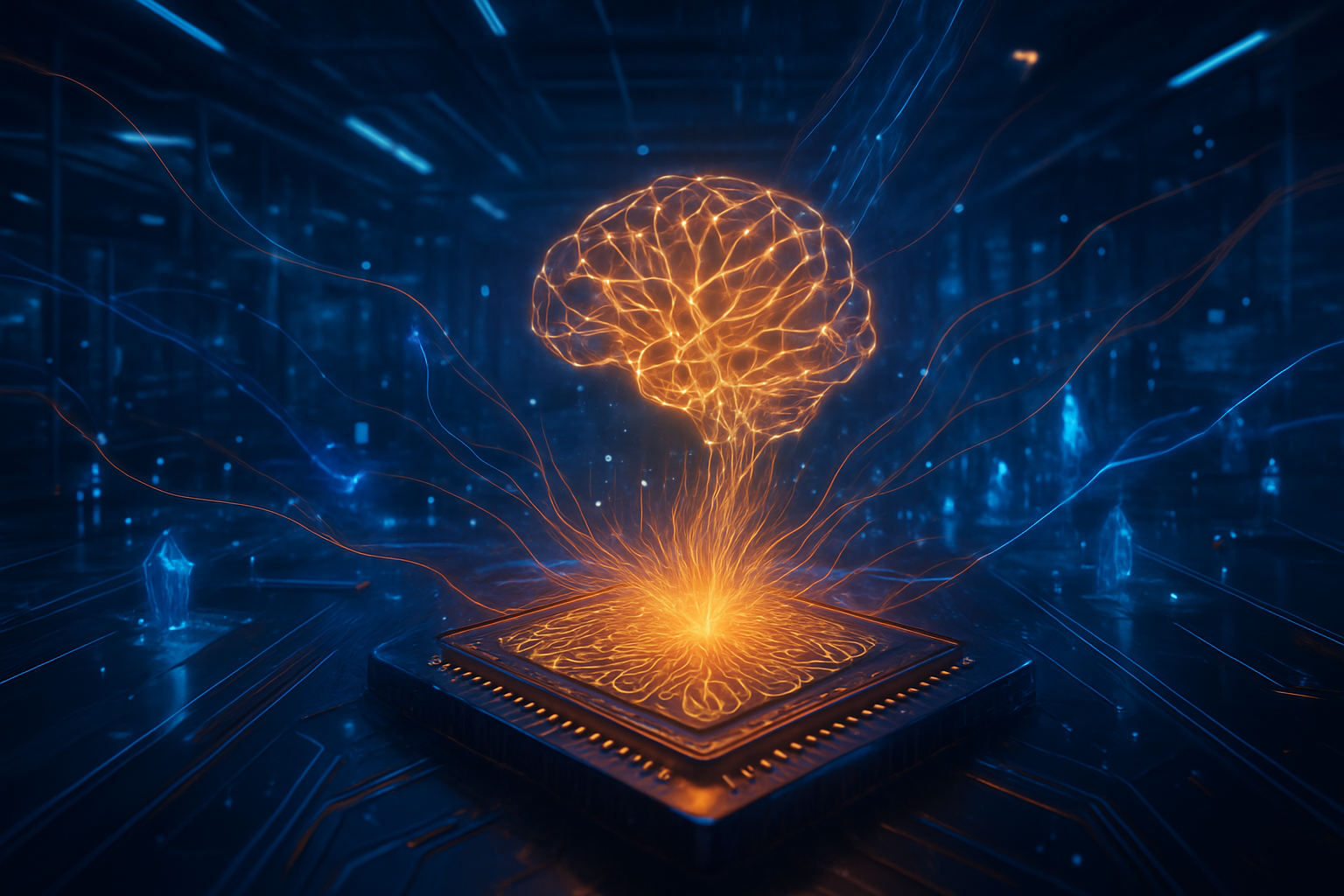
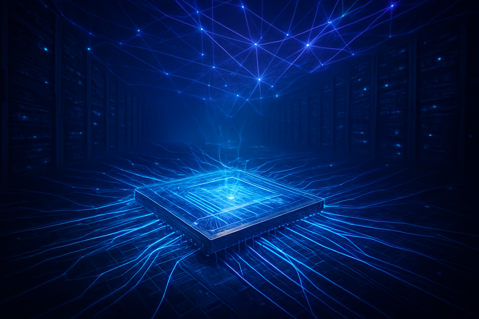
    As of January 8, 2026, the artificial intelligence industry has officially collided with a physical limit known as the "Copper Wall." At data transfer speeds of 224 Gbps and beyond, traditional copper wiring can no longer carry signals more than a few inches without massive signal degradation and unsustainable power consumption. To circumvent this, the world’s leading semiconductor and networking firms have pivoted to Co-Packaged Optics (CPO) and Silicon Photonics, a paradigm shift that integrates fiber-optic communication directly into the chip package. This breakthrough is not just an incremental upgrade; it is the foundational technology enabling the first million-GPU clusters and the training of trillion-parameter AI models.

    The immediate significance of this transition is staggering. By moving the conversion of electrical signals to light (photonics) from separate pluggable modules directly onto the processor or switch substrate, companies are slashing energy consumption by up to 70%. In an era where data center power demands are straining national grids, the ability to move data at 102.4 Tbps while significantly reducing the "tax" of data movement has become the most critical metric in the AI arms race.

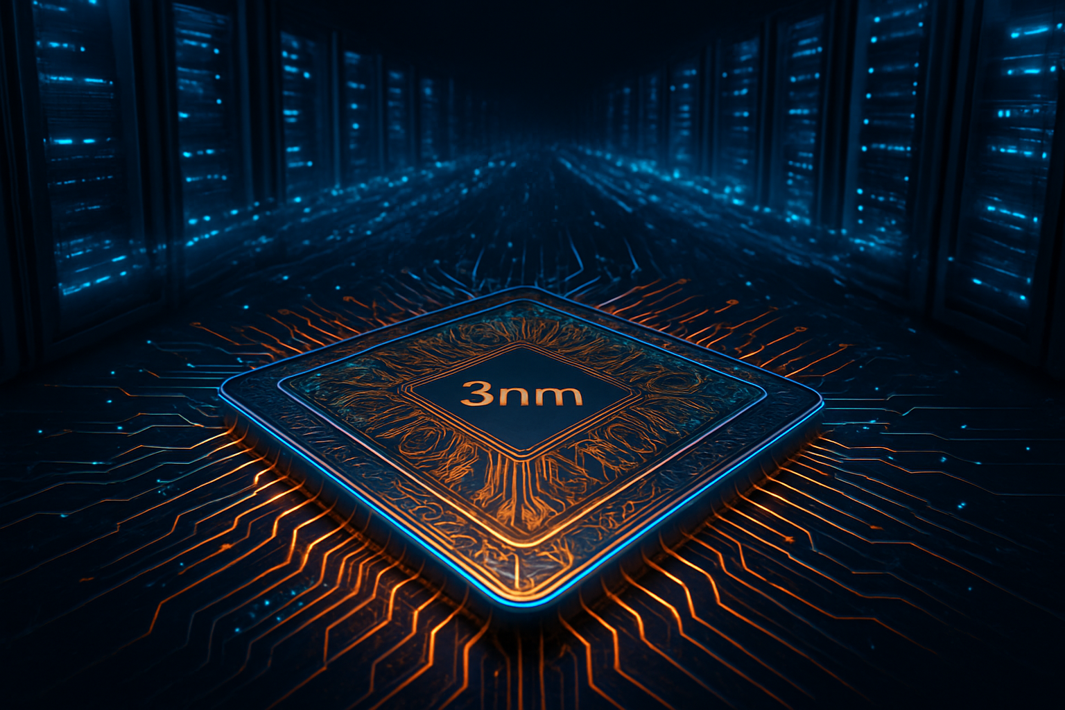
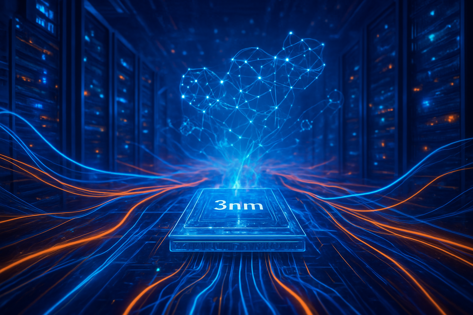
    The technical specifications of the current 2026 hardware generation highlight a massive leap over the pluggable optics of 2024. Broadcom Inc. (NASDAQ: AVGO) has begun volume shipping its "Davisson" Tomahawk 6 switch, the industry’s first 102.4 Tbps Ethernet switch. This device utilizes 16 integrated 6.4 Tbps optical engines, leveraging TSMC’s Compact Universal Photonic Engine (COUPE) technology. Unlike previous generations that relied on power-hungry Digital Signal Processors (DSPs) to push signals through copper traces, CPO systems like Davisson use "Direct Drive" architectures. This eliminates the DSP entirely for short-reach links, bringing energy efficiency down from 15–20 picojoules per bit (pJ/bit) to a mere 5 pJ/bit.

    NVIDIA (NASDAQ: NVDA) has similarly embraced this shift with its Quantum-X800 InfiniBand platform. By utilizing micro-ring modulators, NVIDIA has achieved a bandwidth density of over 1.0 Tbps per millimeter of chip "shoreline"—a five-fold increase over traditional methods. This density is crucial because the physical perimeter of a chip is limited; silicon photonics allows dozens of data channels to be multiplexed onto a single fiber using Wavelength Division Multiplexing (WDM), effectively bypassing the physical constraints of electrical pins.

    The research community has hailed these developments as the "end of the pluggable era." Early reactions from the Open Compute Project (OCP) suggest that the shift to CPO has solved the "Distance-Speed Tradeoff." Previously, high-speed signals were restricted to distances of less than one meter. With silicon photonics, these same signals can now travel up to 2 kilometers with negligible latency (5–10ns compared to the 100ns+ required by DSP-based systems), allowing for "disaggregated" data centers where compute and memory can be located in different racks while behaving as a single monolithic machine.

    The commercial landscape for AI infrastructure is being radically reshaped by this optical transition. Broadcom and NVIDIA have emerged as the primary beneficiaries, having successfully integrated photonics into their core roadmaps. NVIDIA’s latest "Rubin" R100 platform, which entered production in late 2025, makes CPO mandatory for its rack-scale architecture. This move forces competitors to either develop similar in-house photonic capabilities or rely on third-party chiplet providers like Ayar Labs, which recently reached high-volume production of its TeraPHY optical I/O chiplets.

    Intel Corporation (NASDAQ: INTC) has also pivoted its strategy, having divested its traditional pluggable module business to Jabil in late 2024 to focus exclusively on high-value Optical Compute Interconnect (OCI) chiplets. Intel’s OCI is now being sampled by major cloud providers, offering a standardized way to add optical I/O to custom AI accelerators. Meanwhile, Marvell Technology (NASDAQ: MRVL) is positioning itself as the leader in the "Scale-Up" market, using its acquisition of Celestial AI’s photonic fabric to power the next generation of UALink-compatible switches, which are expected to sample in the second half of 2026.

    This shift creates a significant barrier to entry for smaller AI chip startups. The complexity of 2.5D and 3D packaging required to co-package optics with silicon is immense, requiring deep partnerships with foundries like TSMC and specialized OSAT (Outsourced Semiconductor Assembly and Test) providers. Major AI labs, such as OpenAI and Anthropic, are now factoring "optical readiness" into their long-term compute contracts, favoring providers who can offer the lower TCO (Total Cost of Ownership) and higher reliability that CPO provides.

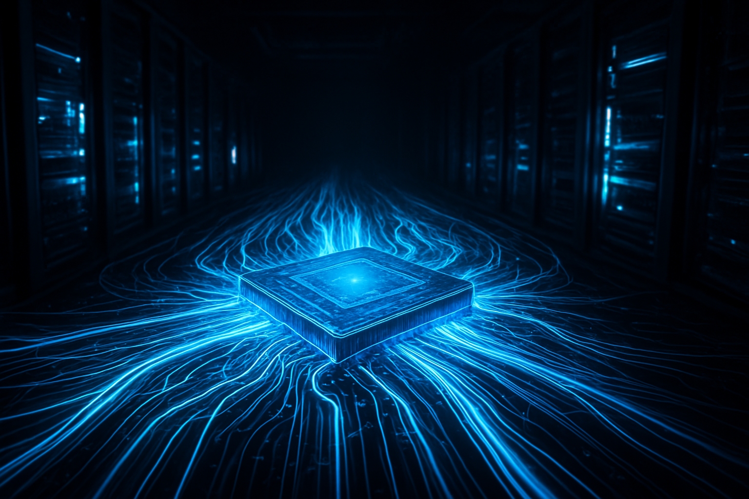
    The wider significance of Co-Packaged Optics lies in its impact on the "Power Wall." A cluster of 100,000 GPUs using traditional interconnects can consume over 60 Megawatts just for data movement. By switching to CPO, data center operators can reclaim that power for actual computation, effectively increasing the "AI work per watt" by a factor of three. This is a critical development for global sustainability goals, as the energy footprint of AI has become a point of intense regulatory scrutiny in early 2026.

    Furthermore, CPO addresses the long-standing issue of reliability in large-scale systems. In the past, the laser—the most failure-prone component of an optical link—was embedded deep inside the chip package, making a single laser failure a catastrophic event for a $40,000 GPU. The 2026 generation of hardware has standardized the External Laser Source (ELSFP), a field-replaceable unit that keeps the heat-generating laser away from the compute silicon. This "pluggable laser" approach combines the reliability of traditional optics with the performance of co-packaging.

    Comparisons are already being drawn to the introduction of High Bandwidth Memory (HBM) in 2015. Just as HBM solved the "Memory Wall" by moving memory closer to the processor, CPO is solving the "Interconnect Wall" by moving the network into the package. This evolution suggests that the future of AI scaling is no longer about making individual chips faster, but about making the entire data center act as a single, fluid fabric of light.

    Looking ahead, the next 24 months will likely see the integration of silicon photonics directly with HBM4. This would allow for "Optical CXL," where a GPU could access memory located hundreds of meters away with the same latency as local on-board memory. Experts predict that by 2027, we will see the first all-optical backplanes, eliminating copper from the data center fabric entirely.

    However, challenges remain. The industry is still debating the standardization of optical interfaces. While the Ultra Accelerator Link (UALink) consortium has made strides, a "standards war" between InfiniBand-centric and Ethernet-centric optical implementations continues. Additionally, the yield rates for 3D-stacked silicon photonics remain lower than traditional CMOS, though they are improving as TSMC and Intel refine their specialized photonic processes.

    The most anticipated development for late 2026 is the deployment of 1.6T and 3.2T optical links per lane. As AI models move toward "World Models" and multi-modal reasoning that requires massive real-time data ingestion, these speeds will transition from a luxury to a necessity. Experts predict that the first "Exascale AI" system, capable of a quintillion operations per second, will be built entirely on a silicon photonics foundation.

    The transition to Co-Packaged Optics and Silicon Photonics represents a watershed moment in the history of computing. By breaking the "Copper Wall," the industry has ensured that the scaling laws of AI can continue for at least another decade. The move from 20 pJ/bit to 5 pJ/bit is not just a technical win; it is an economic and environmental necessity that enables the massive infrastructure projects currently being planned by the world's largest technology companies.

    As we move through 2026, the key metrics to watch will be the volume ramp-up of Broadcom’s Tomahawk 6 and the field performance of NVIDIA’s Rubin platform. If these systems deliver on their promise of 70% power reduction and 10x bandwidth density, the "Optical Era" will be firmly established as the backbone of the AI revolution. The light-speed data center is no longer a laboratory dream; it is the reality of the 2026 AI landscape.


    This content is intended for informational purposes only and represents analysis of current AI developments.

    TokenRing AI delivers enterprise-grade solutions for multi-agent AI workflow orchestration, AI-powered development tools, and seamless remote collaboration platforms.
    For more information, visit https://www.tokenring.ai/.

  • OpenAI Breaks Free: The $10 Billion Amazon ‘Chips-for-Equity’ Deal and the Rise of the XPU

    OpenAI Breaks Free: The $10 Billion Amazon ‘Chips-for-Equity’ Deal and the Rise of the XPU

    In a move that has sent shockwaves through Silicon Valley and the global semiconductor market, OpenAI has finalized a landmark $10 billion strategic agreement with Amazon (NASDAQ: AMZN). This unprecedented "chips-for-equity" arrangement marks a definitive end to OpenAI’s era of near-exclusive reliance on Microsoft (NASDAQ: MSFT) infrastructure. By securing massive quantities of Amazon’s new Trainium 3 chips in exchange for an equity stake, OpenAI is positioning itself as a hardware-agnostic titan, diversifying its compute supply chain at a time when the race for artificial general intelligence (AGI) has become a battle of industrial-scale logistics.

    The deal represents a seismic shift in the AI power structure. For years, NVIDIA (NASDAQ: NVDA) has held a virtual monopoly on the high-end training chips required for frontier models, while Microsoft served as OpenAI’s sole gateway to the cloud. This new partnership provides OpenAI with the "hardware sovereignty" it has long craved, leveraging Amazon’s massive 3nm silicon investments to fuel the training of its next-generation models. Simultaneously, the agreement signals Amazon’s emergence as a top-tier contender in the AI hardware space, proving that its custom silicon can compete with the best in the world.

    The Power of 3nm: Trainium 3’s Efficiency Leap

    The technical heart of this deal is the Trainium 3 chip, which Amazon Web Services (AWS) officially brought to market in late 2025. Manufactured on a cutting-edge 3nm process node, Trainium 3 is designed specifically to solve the "energy wall" currently facing AI developers. The chip boasts a staggering 4x increase in energy efficiency compared to its predecessor, Trainium 2. In an era where data center power consumption is the primary bottleneck for AI scaling, this efficiency gain allows OpenAI to train significantly larger models within the same power footprint.

    Beyond efficiency, the raw performance metrics of Trainium 3 are formidable. Each chip delivers 2.52 PFLOPs of FP8 compute—roughly double the performance of the previous generation—and is equipped with 144GB of high-bandwidth HBM3e memory. This memory architecture provides a 3.9x improvement in bandwidth, ensuring that the massive data throughput required for "reasoning" models like the o1 series is never throttled. To support OpenAI’s massive scale, AWS has deployed these chips in "Trn3 UltraServers," which cluster 144 chips into a single system, capable of being networked into clusters of up to one million units.

    Industry experts have noted that while NVIDIA’s Blackwell architecture remains the gold standard for versatility, Trainium 3 offers a specialized alternative that is highly optimized for the Transformer architectures that OpenAI pioneered. The AI research community has reacted with cautious optimism, noting that a more competitive hardware landscape will likely drive down the "cost per token" for end-users, though it also forces developers to become more proficient in cross-platform software optimization.

    Redrawing the Competitive Map: Beyond the Microsoft-NVIDIA Duopoly

    This deal is a strategic masterstroke for OpenAI, as it effectively plays the tech giants against one another to secure the best possible terms for compute. By diversifying into AWS, OpenAI reduces its exposure to any single point of failure—be it a Microsoft Azure outage or an NVIDIA supply chain bottleneck. For Amazon, the deal is a validation of its long-term investment in Annapurna Labs, the subsidiary responsible for its custom silicon. Securing OpenAI as a flagship customer for Trainium 3 instantly elevates AWS’s status from a general-purpose cloud provider to an AI hardware powerhouse.

    The competitive implications for NVIDIA are significant. While the demand for GPUs still far outstrips supply, the OpenAI-Amazon deal proves that the world’s leading AI lab is no longer willing to pay the "NVIDIA tax" indefinitely. As OpenAI migrates a portion of its training workloads to Trainium 3, it creates a blueprint for other well-funded startups and enterprises to follow. Microsoft, meanwhile, finds itself in a complex position; while it remains OpenAI’s primary partner, it must now compete for OpenAI’s "mindshare" and workloads against a resourced Amazon that is offering equity-backed incentives.

    For Broadcom (NASDAQ: AVGO), the ripple effects are equally lucrative. Alongside the Amazon deal, OpenAI has deepened its partnership with Broadcom to develop a custom "XPU"—a proprietary Accelerated Processing Unit. This "XPU" is designed primarily for high-efficiency inference, intended to run OpenAI’s models in production at a fraction of the cost of general-purpose hardware. By combining Amazon’s training prowess with a Broadcom-designed inference chip, OpenAI is building a vertical stack that spans from silicon design to the end-user application.

    Hardware Sovereignty and the Broader AI Landscape

    The OpenAI-Amazon agreement is more than just a procurement contract; it is a manifesto for the future of AI development. We are entering the era of "hardware sovereignty," where the most advanced AI labs are no longer content to be mere software layers sitting atop third-party chips. Like Apple’s transition to its own M-series silicon, OpenAI is realizing that to achieve the next level of performance, the software and the hardware must be co-designed. This trend is likely to accelerate, with other major players like Google and Meta also doubling down on their internal chip programs.

    This shift also highlights the growing importance of energy as the ultimate currency of the AI age. The 4x efficiency gain of Trainium 3 is not just a technical spec; it is a prerequisite for survival. As AI models begin to require gigawatts of power, the ability to squeeze more intelligence out of every watt becomes the primary competitive advantage. However, this move toward proprietary, siloed hardware ecosystems also raises concerns about "vendor lock-in" and the potential for a fragmented AI landscape where models are optimized for specific clouds and cannot be easily moved.

    Comparatively, this milestone echoes the early days of the internet, when companies moved from renting space in third-party data centers to building their own global fiber networks. OpenAI is now building its own "compute network," ensuring that its path to AGI is not blocked by the commercial interests or supply chain failures of its partners.

    The Road to the XPU and GPT-5

    Looking ahead, the next phase of this strategy will materialize in the second half of 2026, when the first production runs of the OpenAI-Broadcom XPU are expected to ship. This custom chip will likely be the engine behind GPT-5 and subsequent iterations of the o1 reasoning models. Unlike general-purpose GPUs, the XPU will be architected to handle the specific "Chain of Thought" processing that characterizes OpenAI’s latest breakthroughs, potentially offering an order-of-magnitude improvement in inference speed and cost.

    The near-term challenge for OpenAI will be the "software bridge"—ensuring that its massive codebase can run seamlessly across NVIDIA, Amazon, and eventually its own custom silicon. This will require a Herculean effort in compiler and kernel optimization. However, if successful, the payoff will be a model that is not only smarter but significantly cheaper to operate, enabling the deployment of AI agents at a global scale that was previously economically impossible.

    Experts predict that the success of the Trainium 3 deployment will be a bellwether for the industry. If OpenAI can successfully train a frontier model on Amazon’s silicon, it will break the psychological barrier that has kept many developers tethered to NVIDIA’s CUDA ecosystem. The coming months will be a period of intense testing and optimization as OpenAI begins to spin up its first major clusters in AWS data centers.

    A New Chapter in AI History

    The $10 billion deal between OpenAI and Amazon is a definitive turning point in the history of artificial intelligence. It marks the moment when the world’s leading AI laboratory decided to take control of its own physical destiny. By leveraging Amazon’s 3nm Trainium 3 chips and Broadcom’s custom silicon expertise, OpenAI has insulated itself from the volatility of the GPU market and the strategic constraints of a single-cloud partnership.

    The key takeaways from this development are clear: hardware is no longer a commodity; it is a core strategic asset. The efficiency gains of Trainium 3 and the specialized architecture of the upcoming XPU represent a new frontier in AI scaling. For the rest of the industry, the message is equally clear: the "GPU-only" era is ending, and the age of custom, co-designed AI silicon has begun.

    In the coming weeks, the industry will be watching for the first benchmarks of OpenAI models running on Trainium 3. Should these results meet expectations, we may look back at January 2026 as the month the AI hardware monopoly finally cracked, paving the way for a more diverse, efficient, and competitive future for artificial intelligence.


    This content is intended for informational purposes only and represents analysis of current AI developments.

    TokenRing AI delivers enterprise-grade solutions for multi-agent AI workflow orchestration, AI-powered development tools, and seamless remote collaboration platforms.
    For more information, visit https://www.tokenring.ai/.

  • Shattering the Copper Wall: Silicon Photonics Ushers in the Age of Light-Speed AI Clusters

    Shattering the Copper Wall: Silicon Photonics Ushers in the Age of Light-Speed AI Clusters

    As of January 6, 2026, the global technology landscape has reached a definitive crossroads in the evolution of artificial intelligence infrastructure. For decades, the movement of data within the heart of the world’s most powerful computers relied on the flow of electrons through copper wires. However, the sheer scale of modern AI—typified by the emergence of "million-GPU" clusters and the push toward Artificial General Intelligence (AGI)—has officially pushed copper to its physical breaking point. The industry has entered the "Silicon Photonics Era," a transition where light replaces electricity as the primary medium for data center interconnects.

    This shift is not merely a technical upgrade; it is a fundamental re-architecting of how AI models are built and scaled. With the "Copper Wall" rendering traditional electrical signaling inefficient at speeds beyond 224 Gbps, the world’s leading semiconductor and cloud giants have pivoted to optical fabrics. By integrating lasers and photonic circuits directly into the silicon package, the industry has unlocked a 70% reduction in interconnect power consumption while doubling bandwidth, effectively clearing the path for the next decade of AI growth.

    The Physics of the 'Copper Wall' and the Rise of 1.6T Optics

    The technical crisis that precipitated this shift is known as the "Copper Wall." As per-lane speeds reached 224 Gbps in late 2024 and throughout 2025, the reach of passive copper cables plummeted to less than one meter. At these frequencies, electrical signals degrade so rapidly that they can barely traverse a single server rack without massive power-hungry amplification. By early 2025, data center operators reported that the "I/O Tax"—the energy required just to move data between chips—was consuming nearly 30% of total cluster power.

    To solve this, the industry has turned to Co-Packaged Optics (CPO) and Silicon Photonics. Unlike traditional pluggable transceivers that sit at the edge of a switch, CPO moves the optical engine directly onto the processor substrate. This allows for a "shoreline" of high-speed optical I/O that bypasses the energy losses of long electrical traces. In late 2025, the market saw the mass adoption of 1.6T (Terabit) transceivers, which utilize 200G per-lane technology. By early 2026, initial demonstrations of 3.2T links using 400G per-lane technology have already begun, promising to support the massive throughput required for real-time inference on trillion-parameter models.

    The technical community has also embraced Linear-drive Pluggable Optics (LPO) as a bridge technology. By removing the power-intensive Digital Signal Processor (DSP) from the optical module and relying on the host ASIC to drive the signal, LPO has provided a lower-latency, lower-power intermediate step. However, for the most advanced AI clusters, CPO is now considered the "gold standard," as it reduces energy consumption from approximately 15 picojoules per bit (pJ/bit) to less than 5 pJ/bit.

    The New Power Players: NVDA, AVGO, and the Optical Arms Race

    The transition to light has fundamentally shifted the competitive dynamics among semiconductor giants. Nvidia (NASDAQ: NVDA) has solidified its dominance by integrating silicon photonics into its latest Rubin architecture and Quantum-X networking platforms. By utilizing optical NVLink fabrics, Nvidia’s million-GPU clusters can now operate with nanosecond latency, effectively treating an entire data center as a single, massive GPU.

    Broadcom (NASDAQ: AVGO) has emerged as a primary architect of this new era with its Tomahawk 6-Davisson switch, which boasts a staggering 102.4 Tbps throughput and integrated CPO. Broadcom’s success in proving CPO reliability at scale—particularly within the massive AI infrastructures of Meta and Google—has made it the indispensable partner for optical networking. Meanwhile, TSMC (NYSE: TSM) has become the foundational foundry for this transition through its COUPE (Compact Universal Photonic Engine) technology, which allows for the 3D stacking of photonic and electronic circuits, a feat previously thought to be years away from mass production.

    Other key players are carving out critical niches in the optical ecosystem. Marvell (NASDAQ: MRVL), following its strategic acquisition of optical interconnect startups in late 2025, has positioned its Ara 1.6T Optical DSP as the backbone for third-party AI accelerators. Intel (NASDAQ: INTC) has also made a significant comeback in the data center space with its Optical Compute Interconnect (OCI) chiplets. Intel’s unique ability to integrate lasers directly onto the silicon die has enabled "disaggregated" data centers, where compute and memory can be physically separated by over 100 meters without a loss in performance, a capability that is revolutionizing how hyperscalers design their facilities.

    Sustainability and the Global Interconnect Pivot

    The wider significance of the move from copper to light extends far beyond mere speed. In an era where the energy demands of AI have become a matter of national security and environmental concern, silicon photonics offers a rare "win-win" for both performance and sustainability. The 70% reduction in interconnect power provided by CPO is critical for meeting the carbon-neutral goals of tech giants like Microsoft and Amazon, who are currently retrofitting their global data center fleets to support optical fabrics.

    Furthermore, this transition marks the end of the "Compute-Bound" era and the beginning of the "Interconnect-Bound" era. For years, the bottleneck in AI was the speed of the processor itself. Today, the bottleneck is the "fabric"—the ability to move massive amounts of data between thousands of processors simultaneously. By shattering the Copper Wall, the industry has ensured that AI scaling laws can continue to hold true for the foreseeable future.

    However, this shift is not without its concerns. The complexity of manufacturing CPO-based systems is significantly higher than traditional copper-based ones, leading to potential supply chain vulnerabilities. There are also ongoing debates regarding the "serviceability" of integrated optics; if an optical laser fails inside a $40,000 GPU package, the entire unit may need to be replaced, unlike the "hot-swappable" pluggable modules of the past.

    The Road to Petabit Connectivity and Optical Computing

    Looking ahead to the remainder of 2026 and into 2027, the industry is already eyeing the next frontier: Petabit-per-second connectivity. As 3.2T transceivers move into production, researchers are exploring multi-wavelength "comb lasers" that can transmit hundreds of data streams over a single fiber, potentially increasing bandwidth density by another order of magnitude.

    Beyond just moving data, the ultimate goal is Optical Computing—performing mathematical calculations using light itself rather than transistors. While still in the early experimental stages, the integration of photonics into the processor package is the necessary first step toward this "Holy Grail" of computing. Experts predict that by 2028, we may see the first hybrid "Opto-Electronic" processors that perform specific AI matrix multiplications at the speed of light, with virtually zero heat generation.

    The immediate challenge remains the standardization of CPO interfaces. Groups like the OIF (Optical Internetworking Forum) are working feverishly to ensure that components from different vendors can interoperate, preventing the "walled gardens" that could stifle innovation in the optical ecosystem.

    Conclusion: A Bright Future for AI Infrastructure

    The transition from copper to silicon photonics represents one of the most significant architectural shifts in the history of computing. By overcoming the physical limitations of electricity, the industry has laid the groundwork for AGI-scale infrastructure that is faster, more efficient, and more scalable than anything that came before. The "Copper Era," which defined the first fifty years of the digital age, has finally given way to the "Era of Light."

    As we move further into 2026, the key metrics to watch will be the yield rates of CPO-integrated chips and the speed at which 1.6T networking is deployed across global data centers. For AI companies and tech enthusiasts alike, the message is clear: the future of intelligence is no longer traveling through wires—it is moving at the speed of light.


    This content is intended for informational purposes only and represents analysis of current AI developments.

    TokenRing AI delivers enterprise-grade solutions for multi-agent AI workflow orchestration, AI-powered development tools, and seamless remote collaboration platforms.
    For more information, visit https://www.tokenring.ai/.

  • The Silicon Sovereignty Era: Hyperscalers Break NVIDIA’s Grip with 3nm Custom AI Chips

    The Silicon Sovereignty Era: Hyperscalers Break NVIDIA’s Grip with 3nm Custom AI Chips

    The dawn of 2026 has brought a seismic shift to the artificial intelligence landscape, as the world’s largest cloud providers—the hyperscalers—have officially transitioned from being NVIDIA’s (NASDAQ: NVDA) biggest customers to its most formidable architectural rivals. For years, the industry operated under a "one-size-fits-all" GPU paradigm, but a new surge in custom Application-Specific Integrated Circuits (ASICs) has shattered that consensus. Driven by the relentless demand for more efficient inference and the staggering costs of frontier model training, Google, Amazon, and Meta have unleashed a new generation of 3nm silicon that is fundamentally rewriting the economics of AI.

    At the heart of this revolution is a move toward vertical integration that rivals the early days of the mainframe. By designing their own chips, these tech giants are no longer just buying compute; they are engineering it to fit the specific contours of their proprietary models. This strategic pivot is delivering 30% to 40% better price-performance for internal workloads, effectively commoditizing high-end AI compute and providing a critical buffer against the supply chain bottlenecks and premium margins that have defined the NVIDIA era.

    The 3nm Power Play: Ironwood, Trainium3, and the Scaling of MTIA

    The technical specifications of this new silicon class are nothing short of breathtaking. Leading the charge is Google, a subsidiary of Alphabet Inc. (NASDAQ: GOOGL), with its TPU v7p (Ironwood). Built on Taiwan Semiconductor Manufacturing Company’s (NYSE: TSM) cutting-edge 3nm (N3P) process, Ironwood is a dual-chiplet powerhouse featuring a massive 192GB of HBM3E memory. With a memory bandwidth of 7.4 TB/s and a peak performance of 4.6 PFLOPS of dense FP8 compute, the TPU v7p is designed specifically for the "age of inference," where massive context windows and complex reasoning are the new standard. Google has already moved into mass deployment, reporting that over 75% of its Gemini model computations are now handled by its internal TPU fleet.

    Not to be outdone, Amazon.com, Inc. (NASDAQ: AMZN) has officially ramped up production of AWS Trainium3. Also utilizing the 3nm process, Trainium3 packs 144GB of HBM3E and delivers 2.52 PFLOPS of FP8 performance per chip. What sets the AWS offering apart is its "UltraServer" configuration, which interconnects 144 chips into a single, liquid-cooled rack capable of matching NVIDIA’s Blackwell architecture in rack-level performance while offering a significantly more efficient power profile. Meanwhile, Meta Platforms, Inc. (NASDAQ: META) is scaling its Meta Training and Inference Accelerator (MTIA). While its current v2 "Artemis" chips focus on offloading recommendation engines from GPUs, Meta’s 2026 roadmap includes its first dedicated in-house training chip, designed to support the development of Llama 4 and beyond within its massive "Titan" data center clusters.

    These advancements represent a departure from the general-purpose nature of the GPU. While an NVIDIA H100 or B200 is designed to be excellent at almost any parallel task, these custom ASICs are "leaner." By stripping away legacy components and focusing on specific data formats like MXFP8 and MXFP4, and optimizing for specific software frameworks like PyTorch (for Meta) or JAX (for Google), these chips achieve higher throughput per watt. The integration of advanced liquid cooling and proprietary interconnects like Google’s Optical Circuit Switching (OCS) allows these chips to operate in unified domains of nearly 10,000 units, creating a level of "cluster-scale" efficiency that was previously unattainable.

    Disrupting the Monopoly: Market Implications for the GPU Giants

    The immediate beneficiaries of this silicon surge are the hyperscalers themselves, who can now offer AI services at a fraction of the cost of their competitors. AWS has already begun using Trainium3 as a "bargaining chip," implementing price cuts of up to 45% on its NVIDIA-based instances to remain competitive with its own internal hardware. This internal competition is a nightmare scenario for NVIDIA’s margins. While the AI pioneer still dominates the high-end training market, the shift toward inference—projected to account for 70% of all AI workloads in 2026—plays directly into the hands of custom ASIC designers who can optimize for the specific latency and throughput requirements of a deployed model.

    The ripple effects extend to the "enablers" of this custom silicon wave: Broadcom Inc. (NASDAQ: AVGO) and Marvell Technology, Inc. (NASDAQ: MRVL). Broadcom has emerged as the undisputed leader in the custom ASIC space, acting as the primary design partner for Google’s TPUs and Meta’s MTIA. Analysts project Broadcom’s AI semiconductor revenue will hit a staggering $46 billion in 2026, driven by a $73 billion backlog of orders from hyperscalers and firms like Anthropic. Marvell, meanwhile, has secured its place by partnering with AWS on Trainium and Microsoft Corporation (NASDAQ: MSFT) on its Maia accelerators. These design firms provide the critical IP blocks—such as high-speed SerDes and memory controllers—that allow cloud giants to bring chips to market in record time.

    For the broader tech industry, this development signals a fracturing of the AI hardware market. Startups and mid-sized enterprises that were once priced out of the NVIDIA ecosystem are finding a new home in "capacity blocks" of custom silicon. By commoditizing the underlying compute, the hyperscalers are shifting the competitive focus away from who has the most GPUs and toward who has the best data and the most efficient model architectures. This "Silicon Sovereignty" allows the likes of Google and Meta to insulate themselves from the "NVIDIA Tax," ensuring that their massive capital expenditures translate more directly into shareholder value rather than flowing into the coffers of a single hardware vendor.

    A New Architectural Paradigm: Beyond the GPU

    The surge of custom silicon is more than just a cost-saving measure; it is a fundamental shift in the AI landscape. We are moving away from a world where software was written to fit the hardware, and into an era of "hardware-software co-design." When Meta develops a chip in tandem with the PyTorch framework, or Google optimizes its TPU for the Gemini architecture, they achieve a level of vertical integration that mirrors Apple’s success with its M-series silicon. This trend suggests that the "one-size-fits-all" approach of the general-purpose GPU may eventually be relegated to the research lab, while production-scale AI is handled by highly specialized, purpose-built machines.

    However, this transition is not without its concerns. The rise of proprietary silicon could lead to a "walled garden" effect in AI development. If a model is trained and optimized specifically for Google’s TPU v7p, moving that workload to AWS or an on-premise NVIDIA cluster becomes a non-trivial engineering challenge. There are also environmental implications; while these chips are more efficient per token, the sheer scale of deployment is driving unprecedented energy demands. The "Titan" clusters Meta is building in 2026 are gigawatt-scale projects, raising questions about the long-term sustainability of the AI arms race and the strain it puts on national power grids.

    Comparing this to previous milestones, the 2026 silicon surge feels like the transition from CPU-based mining to ASICs in the early days of Bitcoin—but on a global, industrial scale. The era of experimentation is over, and the era of industrial-strength, optimized production has begun. The breakthroughs of 2023 and 2024 were about what AI could do; the breakthroughs of 2026 are about how AI can be delivered to billions of people at a sustainable cost.

    The Horizon: What Comes After 3nm?

    Looking ahead, the roadmap for custom silicon shows no signs of slowing down. As we move toward 2nm and beyond, the focus is expected to shift from raw compute power to "advanced packaging" and "photonic interconnects." Marvell and Broadcom are already experimenting with 3.5D packaging and optical I/O, which would allow chips to communicate at the speed of light, effectively turning an entire data center into a single, giant processor. This would solve the "memory wall" that currently limits the size of the models we can train.

    In the near term, expect to see these custom chips move deeper into the "edge." While 2026 is the year of the data center ASIC, 2027 and 2028 will likely see these same architectures scaled down for use in "AI PCs" and autonomous vehicles. The challenges remain significant—particularly in the realm of software compilers that can automatically optimize code for diverse hardware targets—but the momentum is undeniable. Experts predict that by the end of the decade, over 60% of all AI compute will run on non-NVIDIA hardware, a total reversal of the market dynamics we saw just three years ago.

    Closing the Loop on Custom Silicon

    The mass deployment of Google’s TPU v7p, AWS’s Trainium3, and Meta’s MTIA marks the definitive end of the GPU’s undisputed reign. By taking control of their silicon destiny, the hyperscalers have not only reduced their reliance on a single vendor but have also unlocked a new level of performance that will enable the next generation of "Agentic AI" and trillion-parameter reasoning models. The 30-40% price-performance advantage of these ASICs is the new baseline for the industry, forcing every player in the ecosystem to innovate or be left behind.

    As we move through 2026, the key metrics to watch will be the "utilization rates" of these custom clusters and the speed at which third-party developers adopt the proprietary software stacks required to run on them. The "Silicon Sovereignty" era is here, and it is defined by a simple truth: in the age of AI, the most powerful software is only as good as the silicon it was born to run on. The battle for the future of intelligence is no longer just being fought in the cloud—it’s being fought in the transistor.


    This content is intended for informational purposes only and represents analysis of current AI developments.

    TokenRing AI delivers enterprise-grade solutions for multi-agent AI workflow orchestration, AI-powered development tools, and seamless remote collaboration platforms.
    For more information, visit https://www.tokenring.ai/.

  • OpenAI’s Silicon Sovereignty: The Multi-Billion Dollar Shift to In-House AI Chips

    OpenAI’s Silicon Sovereignty: The Multi-Billion Dollar Shift to In-House AI Chips

    In a move that marks the end of the "GPU-only" era for the world’s leading artificial intelligence lab, OpenAI has officially transitioned into a vertically integrated hardware powerhouse. As of early 2026, the company has solidified its custom silicon strategy, moving beyond its role as a software developer to become a major player in semiconductor design. By forging deep strategic alliances with Broadcom (NASDAQ:AVGO) and TSMC (NYSE:TSM), OpenAI is now deploying its first generation of in-house AI inference chips, a move designed to shatter its near-total dependency on NVIDIA (NASDAQ:NVDA) and fundamentally rewrite the economics of large-scale AI.

    This shift represents a massive gamble on "Silicon Sovereignty"—the idea that to achieve Artificial General Intelligence (AGI), a company must control the entire stack, from the foundational code to the very transistors that execute it. The immediate significance of this development cannot be overstated: by bypassing the "NVIDIA tax" and designing chips tailored specifically for its proprietary Transformer architectures, OpenAI aims to reduce its compute costs by as much as 50%. This cost reduction is essential for the commercial viability of its increasingly complex "reasoning" models, which require significantly more compute per query than previous generations.

    The Architecture of "Project Titan": Inside OpenAI’s First ASIC

    At the heart of OpenAI’s hardware push is a custom Application-Specific Integrated Circuit (ASIC) often referred to internally as "Project Titan." Unlike the general-purpose H100 or Blackwell GPUs from NVIDIA, which are designed to handle a wide variety of tasks from gaming to scientific simulation, OpenAI’s chip is a specialized "XPU" optimized almost exclusively for inference—the process of running a pre-trained model to generate responses. Led by Richard Ho, the former lead of the Google (NASDAQ:GOOGL) TPU program, the engineering team has utilized a systolic array design. This architecture allows data to flow through a grid of processing elements in a highly efficient pipeline, minimizing the energy-intensive data movement that plagues traditional chip designs.

    Technical specifications for the 2026 rollout are formidable. The first generation of chips, manufactured on TSMC’s 3nm (N3) process, incorporates High Bandwidth Memory (HBM3E) to handle the massive parameter counts of the GPT-5 and o1-series models. However, OpenAI has already secured capacity for TSMC’s upcoming A16 (1.6nm) node, which is expected to integrate HBM4 and deliver a 20% increase in power efficiency. Furthermore, OpenAI has opted for an "Ethernet-first" networking strategy, utilizing Broadcom’s Tomahawk switches and optical interconnects. This allows OpenAI to scale its custom silicon across massive clusters without the proprietary lock-in of NVIDIA’s InfiniBand or NVLink technologies.

    The development process itself was a landmark for AI-assisted engineering. OpenAI reportedly used its own "reasoning" models to optimize the physical layout of the chip, achieving area reductions and thermal efficiencies that human engineers alone might have taken months to perfect. This "AI-designing-AI" feedback loop has allowed OpenAI to move from initial concept to a "taped-out" design in record time, surprising many industry veterans who expected the company to spend years in the R&D phase.

    Reshaping the Semiconductor Power Dynamics

    The market implications of OpenAI’s silicon strategy have sent shockwaves through the tech sector. While NVIDIA remains the undisputed king of AI training, OpenAI’s move to in-house inference chips has begun to erode NVIDIA’s dominance in the high-margin inference market. Analysts estimate that by late 2025, inference accounted for over 60% of total AI compute spending, and OpenAI’s transition could represent billions in lost revenue for NVIDIA over the coming years. Despite this, NVIDIA continues to thrive on the back of its Blackwell and upcoming Rubin architectures, though its once-impenetrable "CUDA moat" is showing signs of stress as OpenAI shifts its software to the hardware-agnostic Triton framework.

    The clear winners in this new paradigm are Broadcom and TSMC. Broadcom has effectively become the "foundry for the fabless," providing the essential intellectual property and design platforms that allow companies like OpenAI and Meta (NASDAQ:META) to build custom silicon without owning a single factory. For TSMC, the partnership reinforces its position as the indispensable foundation of the global economy; with its 3nm and 2nm nodes fully booked through 2027, the Taiwanese giant has implemented price hikes that reflect its immense leverage over the AI industry.

    This move also places OpenAI in direct competition with the "hyperscalers"—Google, Amazon (NASDAQ:AMZN), and Microsoft (NASDAQ:MSFT)—all of whom have their own custom silicon programs (TPU, Trainium, and Maia, respectively). However, OpenAI’s strategy differs in its exclusivity. While Amazon and Google rent their chips to third parties via the cloud, OpenAI’s silicon is a "closed-loop" system. It is designed specifically to make running the world’s most advanced AI models economically viable for OpenAI itself, providing a competitive edge in the "Token Economics War" where the company with the lowest marginal cost of intelligence wins.

    The "Silicon Sovereignty" Trend and the End of the Monopoly

    OpenAI’s foray into hardware fits into a broader global trend of "Silicon Sovereignty." In an era where AI compute is viewed as a strategic resource on par with oil or electricity, relying on a single vendor for hardware is increasingly seen as a catastrophic business risk. By designing its own chips, OpenAI is insulating itself from supply chain shocks, geopolitical tensions, and the pricing whims of a monopoly provider. This is a significant milestone in AI history, echoing the moment when early tech giants like IBM (NYSE:IBM) or Apple (NASDAQ:AAPL) realized that to truly innovate in software, they had to master the hardware beneath it.

    However, this transition is not without its concerns. The sheer scale of OpenAI’s ambitions—exemplified by the rumored $500 billion "Stargate" supercomputer project—has raised questions about energy consumption and environmental impact. OpenAI’s roadmap targets a staggering 10 GW to 33 GW of compute capacity by 2029, a figure that would require the equivalent of multiple nuclear power plants to sustain. Critics argue that the race for silicon sovereignty is accelerating an unsustainable energy arms race, even if the custom chips themselves are more efficient than the general-purpose GPUs they replace.

    Furthermore, the "Great Decoupling" from NVIDIA’s CUDA platform marks a shift toward a more fragmented software ecosystem. While OpenAI’s Triton language makes it easier to run models on various hardware, the industry is moving away from a unified standard. This could lead to a world where AI development is siloed within the hardware ecosystems of a few dominant players, potentially stifling the open-source community and smaller startups that cannot afford to design their own silicon.

    The Road to Stargate and Beyond

    Looking ahead, the next 24 months will be critical as OpenAI scales its "Project Titan" chips from initial pilot racks to full-scale data center deployment. The long-term goal is the integration of these chips into "Stargate," the massive AI supercomputer being developed in partnership with Microsoft. If successful, Stargate will be the largest concentrated collection of compute power in human history, providing the "compute-dense" environment necessary for the next leap in AI: models that can reason, plan, and verify their own outputs in real-time.

    Future iterations of OpenAI’s silicon are expected to lean even more heavily into "low-precision" computing. Experts predict that by 2027, OpenAI will be using FP4 or even INT8 precision for its most advanced reasoning tasks, allowing for even higher throughput and lower power consumption. The challenge remains the integration of these chips with emerging memory technologies like HBM4, which will be necessary to keep up with the exponential growth in model parameters.

    Experts also predict that OpenAI may eventually expand its silicon strategy to include "edge" devices. While the current focus is on massive data centers, the ability to run high-quality inference on local hardware—such as AI-integrated laptops or specialized robotics—could be the next frontier. As OpenAI continues to hire aggressively from the silicon teams of Apple, Google, and Intel (NASDAQ:INTC), the boundary between an AI research lab and a semiconductor powerhouse will continue to blur.

    A New Chapter in the AI Era

    OpenAI’s transition to custom silicon is a definitive moment in the evolution of the technology industry. It signals that the era of "AI as a Service" is maturing into an era of "AI as Infrastructure." By taking control of its hardware destiny, OpenAI is not just trying to save money; it is building the foundation for a future where high-level intelligence is a ubiquitous and inexpensive utility. The partnership with Broadcom and TSMC has provided the technical scaffolding for this transition, but the ultimate success will depend on OpenAI's ability to execute at a scale that few companies have ever attempted.

    The key takeaways are clear: the "NVIDIA monopoly" is being challenged not by another chipmaker, but by NVIDIA’s own largest customers. The "Silicon Sovereignty" movement is now the dominant strategy for the world’s most powerful AI labs, and the "Great Decoupling" from proprietary hardware stacks is well underway. As we move deeper into 2026, the industry will be watching closely to see if OpenAI’s custom silicon can deliver on its promise of 50% lower costs and 100% independence.

    In the coming months, the focus will shift to the first performance benchmarks of "Project Titan" in production environments. If these chips can match or exceed the performance of NVIDIA’s Blackwell in real-world inference tasks, it will mark the beginning of a new chapter in AI history—one where the intelligence of the model is inseparable from the silicon it was born to run on.


    This content is intended for informational purposes only and represents analysis of current AI developments.

    TokenRing AI delivers enterprise-grade solutions for multi-agent AI workflow orchestration, AI-powered development tools, and seamless remote collaboration platforms.
    For more information, visit https://www.tokenring.ai/.

  • The Speed of Light: Silicon Photonics and the End of the Copper Era in AI Data Centers

    The Speed of Light: Silicon Photonics and the End of the Copper Era in AI Data Centers

    As the calendar turns to 2026, the artificial intelligence industry has arrived at a pivotal architectural crossroads. For decades, the movement of data within computers has relied on the flow of electrons through copper wiring. However, as AI clusters scale toward the "million-GPU" milestone, the physical limits of electricity—long whispered about as the "Copper Wall"—have finally been reached. In the high-stakes race to build the infrastructure for Artificial General Intelligence (AGI), the industry is officially abandoning traditional electrical interconnects in favor of Silicon Photonics and Co-Packaged Optics (CPO).

    This transition marks one of the most significant shifts in computing history. By integrating laser-based data transmission directly onto the silicon chip, industry titans like Broadcom (NASDAQ:AVGO) and NVIDIA (NASDAQ:NVDA) are enabling petabit-per-second connectivity with energy efficiency that was previously thought impossible. The arrival of these optical "superhighways" in early 2026 signals the end of the copper era in high-performance data centers, effectively decoupling bandwidth growth from the crippling power constraints that threatened to stall AI progress.

    Breaking the Copper Wall: The Technical Leap to CPO

    The technical crisis necessitating this shift is rooted in the physics of 224 Gbps signaling. At these speeds, the reach of traditional passive copper cables has shrunk to less than one meter, and the power required to force electrical signals through these wires has skyrocketed. In early 2025, data center operators reported that interconnects were consuming nearly 30% of total cluster power. The solution, arriving in volume this year, is Co-Packaged Optics. Unlike traditional pluggable transceivers that sit on the edge of a switch, CPO brings the optical engine directly into the chip's package.

    Broadcom (NASDAQ:AVGO) has set the pace with its 2026 flagship, the Tomahawk 6-Davisson switch. Boasting a staggering 102.4 Terabits per second (Tbps) of aggregate capacity, the Davisson utilizes TSMC (NYSE:TSM) COUPE technology to stack photonic engines directly onto the switching silicon. This integration reduces data transmission energy by over 70%, moving from roughly 15 picojoules per bit (pJ/bit) in traditional systems to less than 5 pJ/bit. Meanwhile, NVIDIA (NASDAQ:NVDA) has launched its Quantum-X Photonics InfiniBand platform, specifically designed to link its "million-GPU" clusters. These systems replace bulky copper cables with thin, liquid-cooled fiber optics that provide 10x better network resiliency and nanosecond-level latency.

    The AI research community has reacted with a mix of relief and awe. Experts at leading labs note that without CPO, the "scaling laws" of large language models would have hit a hard ceiling due to I/O bottlenecks. The ability to move data at light speed across a massive fabric allows a million GPUs to behave as a single, coherent computational entity. This technical breakthrough is not merely an incremental upgrade; it is the foundational plumbing required for the next generation of multi-trillion parameter models.

    The New Power Players: Market Shifts and Strategic Moats

    The shift to Silicon Photonics is fundamentally reordering the semiconductor landscape. Broadcom (NASDAQ:AVGO) has emerged as the clear leader in the Ethernet-based merchant silicon market, leveraging its $73 billion AI backlog to solidify its role as the primary alternative to NVIDIA’s proprietary ecosystem. By providing custom CPO-integrated ASICs to hyperscalers like Meta (NASDAQ:META) and OpenAI, Broadcom is helping these giants build "hardware moats" that are optimized for their specific AI architectures, often achieving 30-50% better performance-per-watt than general-purpose hardware.

    NVIDIA (NASDAQ:NVDA), however, remains the dominant force in the "scale-up" fabric. By vertically integrating CPO into its NVLink and InfiniBand stacks, NVIDIA is effectively locking customers into a high-performance ecosystem where the network is as inseparable from the GPU as the memory. This strategy has forced competitors like Marvell (NASDAQ:MRVL) and Cisco (NASDAQ:CSCO) to innovate rapidly. Marvell, in particular, has positioned itself as a key challenger following its acquisition of Celestial AI, offering a "Photonic Fabric" that allows for optical memory pooling—a technology that lets thousands of GPUs share a massive, low-latency memory pool across an entire data center.

    This transition has also created a "paradox of disruption" for traditional optical component makers like Lumentum (NASDAQ:LITE) and Coherent (NYSE:COHR). While the traditional pluggable module business is being cannibalized by CPO, these companies have successfully pivoted to become "laser foundries." As the primary suppliers of the high-powered Indium Phosphide (InP) lasers required for CPO, their role in the supply chain has shifted from assembly to critical component manufacturing, making them indispensable partners to the silicon giants.

    A Global Imperative: Energy, Sustainability, and the Race for AGI

    Beyond the technical and market implications, the move to Silicon Photonics is a response to a looming environmental and societal crisis. By 2026, global data center electricity usage is projected to reach approximately 1,050 terawatt-hours, nearly the total power consumption of Japan. In tech hubs like Northern Virginia and Ireland, "grid nationalism" has become a reality, with local governments restricting new data center permits due to massive power spikes. Silicon Photonics provides a critical "pressure valve" for these grids by drastically reducing the energy overhead of AI training.

    The societal significance of this transition cannot be overstated. We are witnessing the construction of "Gigafactory" scale clusters, such as xAI’s Colossus 2 and Microsoft’s (NASDAQ:MSFT) Fairwater site, which are designed to house upwards of one million GPUs. These facilities are the physical manifestations of the race for AGI. Without the energy savings provided by optical interconnects, the carbon footprint and water usage (required for cooling) of these sites would be politically and environmentally untenable. CPO is effectively the "green technology" that allows the AI revolution to continue scaling.

    Furthermore, this shift highlights the world's extreme dependence on TSMC (NYSE:TSM). As the only foundry currently capable of the ultra-precise 3D chip-stacking required for CPO, TSMC has become the ultimate bottleneck in the global AI supply chain. The complexity of manufacturing these integrated photonic/electronic packages means that any disruption at TSMC’s advanced packaging facilities in 2026 could stall global AI development more effectively than any previous chip shortage.

    The Horizon: Optical Computing and the Post-Silicon Future

    Looking ahead, 2026 is just the beginning of the optical revolution. While CPO currently focuses on data transmission, the next frontier is optical computation. Startups like Lightmatter are already sampling "Photonic Compute Units" that perform matrix multiplications using light rather than electricity. These chips promise a 100x improvement in efficiency for specific AI inference tasks, potentially replacing traditional electrical transistors in the late 2020s.

    In the near term, the industry is already pathfinding for the 448G-per-lane standard. This will involve the use of plasmonic modulators—ultra-compact devices that can operate at speeds exceeding 145 GHz while consuming less than 1 pJ/bit. Experts predict that by 2028, the "Copper Era" will be a distant memory even in consumer-level networking, as the cost of silicon photonics drops and the technology trickles down from the data center to the edge.

    The challenges remains significant, particularly regarding the reliability of laser sources and the sheer complexity of field-repairing co-packaged systems. However, the momentum is irreversible. The industry has realized that the only way to keep pace with the exponential growth of AI is to stop fighting the physics of electrons and start harnessing the speed of light.

    Summary: A New Architecture for a New Intelligence

    The transition to Silicon Photonics and Co-Packaged Optics in 2026 represents a fundamental decoupling of computing power from energy consumption. By shattering the "Copper Wall," companies like Broadcom, NVIDIA, and TSMC have cleared the path for the million-GPU clusters that will likely train the first true AGI models. The key takeaways from this shift include a 70% reduction in interconnect power, the rise of custom optical ASICs for major AI labs, and a renewed focus on data center sustainability.

    In the history of computing, we will look back at 2026 as the year the industry "saw the light." The long-term impact will be felt in every corner of society, from the speed of AI breakthroughs to the stability of our global power grids. In the coming months, watch for the first performance benchmarks from xAI’s million-GPU cluster and further announcements from the OIF (Optical Internetworking Forum) regarding the 448G standard. The era of copper is over; the era of the optical supercomputer has begun.


    This content is intended for informational purposes only and represents analysis of current AI developments.

    TokenRing AI delivers enterprise-grade solutions for multi-agent AI workflow orchestration, AI-powered development tools, and seamless remote collaboration platforms. For more information, visit https://www.tokenring.ai/.

  • The Speed of Light: Silicon Photonics Shatters the AI Interconnect Bottleneck

    The Speed of Light: Silicon Photonics Shatters the AI Interconnect Bottleneck

    As the calendar turns to January 1, 2026, the artificial intelligence industry has reached a pivotal infrastructure milestone: the definitive end of the "Copper Era" in high-performance data centers. Over the past 18 months, the relentless pursuit of larger Large Language Models (LLMs) and more complex generative agents has pushed traditional electrical networking to its physical breaking point. The solution, long-promised but only recently perfected, is Silicon Photonics—the integration of laser-based data transmission directly into the silicon chips that power AI.

    This transition marks a fundamental shift in how AI clusters are built. By replacing copper wires with pulses of light for chip-to-chip communication, the industry has successfully bypassed the "interconnect bottleneck" that threatened to stall the scaling of AI. This development is not merely an incremental speed boost; it is a total redesign of the data center's nervous system, enabling million-GPU clusters to operate as a single, cohesive supercomputer with unprecedented efficiency and bandwidth.

    Breaking the Copper Wall: Technical Specifications of the Optical Revolution

    The primary driver for this shift is a physical phenomenon known as the "Copper Wall." As data rates reached 224 Gbps per lane in late 2024 and throughout 2025, the reach of passive copper cables plummeted to less than one meter. To send electrical signals any further required massive amounts of power for amplification and retiming, leading to a scenario where interconnects accounted for nearly 30% of total data center energy consumption. Furthermore, "shoreline bottlenecks"—the limited physical space on the edge of a GPU for electrical pins—prevented hardware designers from adding more I/O to match the increasing compute power of the chips.

    The technical breakthrough that solved this is Co-Packaged Optics (CPO). In early 2025, Nvidia (NASDAQ: NVDA) unveiled its Quantum-X InfiniBand and Spectrum-X Ethernet platforms, which moved the optical conversion process inside the processor package using TSMC’s (NYSE: TSM) Compact Universal Photonic Engine (COUPE) technology. These systems support up to 144 ports of 800 Gb/s, delivering a staggering 115 Tbps of total throughput. By integrating the laser and optical modulators directly onto the chiplet, Nvidia reduced power consumption by 3.5x compared to traditional pluggable modules, while simultaneously cutting latency from microseconds to nanoseconds.

    Unlike previous approaches that relied on external pluggable transceivers, the new generation of Optical I/O, such as Intel’s (NASDAQ: INTC) Optical Compute Interconnect (OCI) chiplet, allows for bidirectional data transfer at 4 Tbps over distances of up to 100 meters. These chiplets operate at just 5 pJ/bit (picojoules per bit), a massive improvement over the 15 pJ/bit required by legacy systems. This allows AI researchers to build "disaggregated" data centers where memory and compute can be physically separated by dozens of meters without sacrificing the speed required for real-time model training.

    The Trillion-Dollar Fabric: Market Impact and Strategic Positioning

    The shift to Silicon Photonics has triggered a massive realignment among tech giants and semiconductor firms. In a landmark move in December 2025, Marvell (NASDAQ: MRVL) completed its acquisition of startup Celestial AI in a deal valued at over $5 billion. This acquisition gave Marvell control over the "Photonic Fabric," a technology that allows GPUs to access massive pools of external memory with the same speed as if that memory were on the chip itself. This has positioned Marvell as the primary challenger to Nvidia’s dominance in custom AI silicon, particularly for hyperscalers like Amazon (NASDAQ: AMZN) and Meta (NASDAQ: META) who are looking to build their own bespoke AI accelerators.

    Broadcom (NASDAQ: AVGO) has also solidified its position by moving into volume production of its Tomahawk 6-Davisson switch. Announced in late 2025, the Tomahawk 6 is the world’s first 102.4 Tbps Ethernet switch featuring integrated CPO. By successfully deploying these switches in Meta's massive AI clusters, Broadcom has proven that silicon photonics can meet the reliability standards required for 24/7 industrial AI operations. This has put immense pressure on traditional networking companies that were slower to pivot away from pluggable optics.

    For AI labs like OpenAI and Anthropic, this technological leap means the "scaling laws" can continue to hold. The ability to connect hundreds of thousands of GPUs into a single fabric allows for the training of models with tens of trillions of parameters—models that were previously impossible to train due to the latency of copper-based networks. The competitive advantage has shifted toward those who can secure not just the fastest GPUs, but the most efficient optical fabrics to link them.

    A Sustainable Path to AGI: Wider Significance and Concerns

    The broader significance of Silicon Photonics lies in its impact on the environmental and economic sustainability of AI. Before the widespread adoption of CPO, the power trajectory of AI data centers was unsustainable, with some estimates suggesting they would consume 10% of global electricity by 2030. Silicon Photonics has bent that curve. By reducing the energy required for data movement by over 60%, the industry has found a way to continue scaling compute power while keeping energy growth manageable.

    This transition also marks the realization of "The Rack is the Computer" philosophy. In the past, a data center was a collection of individual servers. Today, thanks to the high-bandwidth, low-latency reach of optical interconnects, an entire rack—or even multiple rows of racks—functions as a single, giant processor. This architectural shift is a prerequisite for the next stage of AI development: distributed reasoning engines that require massive, instantaneous data exchange across thousands of nodes.

    However, the shift is not without its concerns. The complexity of manufacturing silicon photonics—which requires the precise alignment of lasers and optical fibers at a microscopic scale—has created a new set of supply chain vulnerabilities. The industry is now heavily dependent on a few specialized packaging facilities, primarily those owned by TSMC and Intel. Any disruption in this specialized supply chain could stall the global rollout of nextgeneration AI infrastructure more effectively than a shortage of raw compute chips.

    The Road to 2030: Future Developments in Light-Based Computing

    Looking ahead, the next frontier is the "All-Optical Data Center." While we have successfully transitioned the interconnects to light, the actual processing of data still occurs electrically within the transistors. Experts predict that by 2028, we will see the first commercial "Optical Compute" chips from companies like Lightmatter, which use light not just to move data, but to perform the matrix multiplications at the heart of AI workloads. Lightmatter’s Passage M1000 platform, which already supports 114 Tbps of bandwidth, is a precursor to this future.

    Near-term developments will focus on reducing power consumption even further, targeting the "sub-1 pJ/bit" threshold. This will likely involve 3D stacking of photonic layers directly on top of logic layers, eliminating the need for any horizontal electrical traces. As these technologies mature, we expect to see Silicon Photonics migrate from the data center into edge devices, enabling high-performance AI in autonomous vehicles and advanced robotics where power and heat are strictly limited.

    The primary challenge remaining is the "Laser Problem." Currently, most systems use external laser sources because lasers generate heat that can interfere with sensitive logic circuits. Researchers are working on "quantum dot" lasers that can be grown directly on silicon, which would further simplify the architecture and reduce costs. If successful, this would make Silicon Photonics as ubiquitous as the transistor itself.

    Summary: The New Foundation of Artificial Intelligence

    The successful integration of Silicon Photonics into the AI stack represents one of the most significant engineering achievements of the 2020s. By breaking the copper wall, the industry has cleared the path for the next generation of AI clusters, moving from the gigabit era into a world of petabit-per-second connectivity. The key takeaways from this transition are the massive gains in power efficiency, the shift toward disaggregated data center architectures, and the consolidation of market power among those who control the optical fabric.

    As we move through 2026, the industry will be watching for the first "million-GPU" clusters powered entirely by CPO. These facilities will serve as the proving ground for the most advanced AI models ever conceived. Silicon Photonics has effectively turned the "interconnect bottleneck" from a looming crisis into a solved problem, ensuring that the only limit to AI’s growth is the human imagination—and the availability of clean energy to power the lasers.


    This content is intended for informational purposes only and represents analysis of current AI developments.

    TokenRing AI delivers enterprise-grade solutions for multi-agent AI workflow orchestration, AI-powered development tools, and seamless remote collaboration platforms.
    For more information, visit https://www.tokenring.ai/.

  • Broadcom’s AI Nervous System: Record $18B Revenue and a $73B Backlog Redefine the Infrastructure Race

    Broadcom’s AI Nervous System: Record $18B Revenue and a $73B Backlog Redefine the Infrastructure Race

    Broadcom Inc. (NASDAQ:AVGO) has solidified its position as the indispensable architect of the generative AI era, reporting record-breaking fiscal fourth-quarter 2025 results that underscore a massive shift in data center architecture. On December 11, 2025, the semiconductor giant announced quarterly revenue of $18.02 billion—a 28.2% year-over-year increase—driven primarily by an "inflection point" in AI networking demand and custom silicon accelerators. As hyperscalers race to build massive AI clusters, Broadcom has emerged as the primary provider of the "nervous system" connecting these digital brains, boasting a staggering $73 billion AI-related order backlog that stretches well into 2027.

    The significance of these results extends beyond mere revenue growth; they represent a fundamental transition in how AI infrastructure is built. With AI semiconductor revenue surging 74% to $6.5 billion in the quarter alone, Broadcom is no longer just a component supplier but a systems-level partner for the world’s largest tech entities. The company’s ability to secure a $10 billion order from OpenAI for its "Titan" inference chips and an $11 billion follow-on commitment from Anthropic highlights a growing trend: the world’s most advanced AI labs are moving away from off-the-shelf solutions in favor of bespoke silicon designed in tandem with Broadcom’s engineering teams.

    The 3nm Frontier: Tomahawk 6 and the Rise of Custom XPUs

    At the heart of Broadcom’s technical dominance is its aggressive transition to the 3nm process node, which has birthed a new generation of networking and compute silicon. The standout announcement was the volume production of the Tomahawk 6 (TH6) switch, the world’s first 102.4 Terabits per second (Tbps) switching ASIC. Utilizing 200G PAM4 SerDes technology, the TH6 doubles the bandwidth of its predecessor while reducing power consumption per bit by 40%. This allows hyperscalers to scale AI clusters to over one million accelerators (XPUs) within a single Ethernet fabric—a feat previously thought impossible with traditional networking standards.

    Complementing the switching power is the Jericho 4 router, which introduces "HyperPort" technology. This innovation allows for 3.2 Tbps logical ports, enabling lossless data transfer across distances of up to 60 miles. This is critical for the modern AI landscape, where power constraints often force companies to split massive training clusters across multiple physical data centers. By using Jericho 4, companies can link these disparate sites as if they were a single logical unit. On the compute side, Broadcom’s partnership with Alphabet Inc. (NASDAQ:GOOGL) has yielded the 7th-generation "Ironwood" TPU, while work with Meta Platforms, Inc. (NASDAQ:META) on the "Santa Barbara" ASIC project focuses on high-power, liquid-cooled designs capable of handling the next generation of Llama models.

    The Ethernet Rebellion: Disrupting the InfiniBand Monopoly

    Broadcom’s record results signal a major shift in the competitive landscape of AI networking, posing a direct challenge to the dominance of Nvidia Corporation (NASDAQ:NVDA) and its proprietary InfiniBand technology. For years, InfiniBand was the gold standard for AI due to its low latency, but as clusters grow to hundreds of thousands of GPUs, the industry is pivoting toward open Ethernet standards. Broadcom’s Tomahawk and Jericho series are the primary beneficiaries of this "Ethernet Rebellion," offering a more scalable and cost-effective alternative that integrates seamlessly with existing data center management tools.

    This strategic positioning has made Broadcom the "premier arms dealer" for the hyperscale elite. By providing the underlying fabric for Google’s TPUs and Meta’s MTIA chips, Broadcom is enabling these giants to reduce their reliance on external GPU vendors. The recent $10 billion commitment from OpenAI for its custom "Titan" silicon further illustrates this shift; as AI labs seek to optimize for specific workloads like inference, Broadcom’s custom XPU (AI accelerator) business provides the specialized hardware that generic GPUs cannot match. This creates a powerful moat: Broadcom is not just selling chips; it is selling the ability for tech giants to maintain their own competitive sovereignty.

    The Margin Debate: Revenue Volume vs. the "HBM Tax"

    Despite the stellar revenue figures, Broadcom’s report introduced a point of contention for investors: a projected 100-basis-point sequential decline in gross margins for the first quarter of 2026. This margin compression is a direct result of the company’s success in "AI systems" integration. As Broadcom moves from selling standalone ASICs to delivering full-rack solutions, it must incorporate third-party components like High Bandwidth Memory (HBM) from suppliers like SK Hynix or Samsung Electronics (KRX:005930). These components are essentially "passed through" to the customer at cost, which inflates total revenue (the top line) but dilutes the gross margin percentage.

    Analysts from firms like Goldman Sachs Group Inc. (NYSE:GS) and JPMorgan Chase & Co. (NYSE:JPM) have characterized this as a "margin reset" rather than a structural weakness. While a 77.9% gross margin is expected to dip toward 76.9% in the near term, the sheer volume of the $73 billion backlog suggests that absolute profit dollars will continue to climb. Furthermore, Broadcom’s software division, bolstered by the integration of VMware, continues to provide a high-margin buffer. The company reported that VMware’s transition to a subscription-based model is ahead of schedule, contributing significantly to the $63.9 billion in total fiscal 2025 revenue and ensuring that overall EBITDA margins remain resilient at approximately 67%.

    Looking Ahead: 1.6T Networking and the Fifth Customer

    The future for Broadcom appears anchored in the rapid adoption of 1.6T Ethernet networking, which is expected to become the industry standard by late 2026. The company is already sampling its next-generation optical interconnects, which replace copper wiring with light-based data transfer to overcome the physical limits of electrical signaling at high speeds. This will be essential as AI models continue to grow in complexity, requiring even faster communication between the thousands of chips working in parallel.

    Perhaps the most intriguing development for 2026 is the addition of a "fifth major custom XPU customer." While Broadcom has not officially named the entity, the company confirmed a $1 billion initial order for delivery in late 2026. Industry speculation points toward a major consumer electronics or cloud provider looking to follow the lead of Google and Meta. As this mystery partner ramps up, Broadcom’s custom silicon business is expected to represent an even larger share of its semiconductor solutions, potentially reaching 50% of the segment's revenue within the next two years.

    Conclusion: The Foundation of the AI Economy

    Broadcom’s fiscal Q4 2025 results mark a definitive moment in the history of the semiconductor industry. By delivering $18 billion in quarterly revenue and securing a $73 billion backlog, the company has proven that it is the foundational bedrock upon which the AI economy is being built. While the market may grapple with the short-term implications of margin compression due to the shift toward integrated systems, the long-term trajectory is clear: the demand for high-speed, scalable, and custom-tailored AI infrastructure shows no signs of slowing down.

    As we move into 2026, the tech industry will be watching Broadcom’s ability to execute on its massive backlog and its success in onboarding its fifth major custom silicon partner. With the Tomahawk 6 and Jericho 4 chips setting new benchmarks for what is possible in data center networking, Broadcom has successfully positioned itself at the center of the AI universe. For investors and industry observers alike, the message from Broadcom’s headquarters is unmistakable: the AI revolution will be networked, and that network will run on Broadcom silicon.


    This content is intended for informational purposes only and represents analysis of current AI developments.

    TokenRing AI delivers enterprise-grade solutions for multi-agent AI workflow orchestration, AI-powered development tools, and seamless remote collaboration platforms.
    For more information, visit https://www.tokenring.ai/.

  • The Light Speed Revolution: Silicon Photonics Hits Commercial Prime as Marvell and Broadcom Reshape AI Infrastructure

    The Light Speed Revolution: Silicon Photonics Hits Commercial Prime as Marvell and Broadcom Reshape AI Infrastructure

    The artificial intelligence industry has reached a pivotal infrastructure milestone as silicon photonics transitions from a long-promised laboratory curiosity to the backbone of global data centers. In a move that signals the end of the "copper era" for high-performance computing, Marvell Technology (NASDAQ: MRVL) officially announced its definitive agreement to acquire Celestial AI on December 2, 2025, for an initial value of $3.25 billion. This acquisition, coupled with Broadcom’s (NASDAQ: AVGO) staggering record of $20 billion in AI hardware revenue for fiscal year 2025, confirms that light-based interconnects are no longer a luxury—they are a necessity for the next generation of generative AI.

    The commercial breakthrough comes at a critical time when traditional electrical signaling is hitting physical limits. As AI models like OpenAI’s "Titan" project demand unprecedented levels of data throughput, the industry is shifting toward optical solutions to solve the "memory wall"—the bottleneck where processors spend more time waiting for data than computing it. This convergence of Marvell’s strategic M&A and Broadcom’s dominant market performance marks the beginning of a new epoch in AI hardware, where silicon photonics provides the massive bandwidth and energy efficiency required to sustain the current pace of AI scaling.

    Breaking the Memory Wall: The Technical Leap to Photonic Fabrics

    The centerpiece of this technological shift is the "Photonic Fabric," a proprietary architecture developed by Celestial AI that Marvell is now integrating into its portfolio. Unlike traditional pluggable optics that sit at the edge of a motherboard, Celestial AI’s technology utilizes an Optical Multi-Chip Interconnect Bridge (OMIB). This allows for 3D packaging where optical interconnects are placed directly on the silicon substrate alongside AI accelerators (XPUs) and High Bandwidth Memory (HBM). By using light to transport data across these components, the Photonic Fabric delivers 25 times greater bandwidth while reducing latency and power consumption by a factor of ten compared to existing copper-based solutions.

    Broadcom (NASDAQ: AVGO) has simultaneously pushed the envelope with its own optical innovations, recently unveiling the Tomahawk 6 "Davidson" switch. This 102.4 Tbps Ethernet switch is the first to utilize 200G-per-lane Co-Packaged Optics (CPO). By integrating the optical engines directly into the switch package, Broadcom has slashed the energy required to move a bit of data, a feat previously thought impossible at these speeds. The industry's move to 1.6T and eventually 3.2T interconnects is now being realized through these advancements in silicon photonics, allowing hundreds of individual chips to function as a single, massive "virtual" processor.

    This shift represents a fundamental departure from the "scale-out" networking of the past decade. Previously, data centers connected clusters of servers using standard networking cables, which introduced significant lag. The new silicon photonics paradigm enables "scale-up" architectures, where the entire rack—or even multiple racks—is interconnected via a seamless web of light. This allows for near-instantaneous memory sharing across thousands of GPUs, effectively neutralizing the physical distance between chips and allowing larger models to be trained in a fraction of the time.

    Initial reactions from the AI research community have been overwhelmingly positive, with experts noting that these hardware breakthroughs are the "missing link" for trillion-parameter models. By moving the data bottleneck from the electrical domain to the optical domain, engineers can finally match the raw processing power of modern chips with a communication infrastructure that can keep up. The integration of 3nm Digital Signal Processors (DSPs) like Broadcom’s Sian3 further optimizes this ecosystem, ensuring that the transition to light is as power-efficient as possible.

    Market Dominance and the New Competitive Landscape

    The acquisition of Celestial AI positions Marvell Technology (NASDAQ: MRVL) as a formidable challenger to the established order of AI networking. By securing the Photonic Fabric technology, Marvell is targeting a $1 billion annualized revenue run rate for its optical business by 2029. This move is a direct shot across the bow of Nvidia (NASDAQ: NVDA) (NASDAQ: NVDA), which has traditionally dominated the AI interconnect space with its proprietary NVLink technology. Marvell’s strategy is to offer an open, high-performance alternative that appeals to hyperscalers like Google (NASDAQ: GOOGL) and Meta (NASDAQ: META), who are increasingly looking to decouple their hardware stacks from single-vendor ecosystems.

    Broadcom, meanwhile, has solidified its status as the "arms dealer" of the AI era. With AI revenue surging to $20 billion in 2025—a 65% year-over-year increase—Broadcom’s dominance in custom ASICs and high-end switching is unparalleled. Their record Q4 revenue of $6.5 billion was largely driven by the massive deployment of custom AI accelerators for major cloud providers. By leading the charge in Co-Packaged Optics, Broadcom is ensuring that it remains the primary partner for any firm building a massive AI cluster, effectively gatekeeping the physical layer of the AI revolution.

    The competitive implications for startups and smaller AI labs are profound. As the cost of building state-of-the-art optical infrastructure rises, the barrier to entry for training "frontier" models becomes even higher. However, the availability of standardized silicon photonics products from Marvell and Broadcom could eventually democratize access to high-performance interconnects, allowing smaller players to build more efficient clusters using off-the-shelf components rather than expensive, proprietary systems.

    For the tech giants, this development is a strategic win. Companies like Meta (NASDAQ: META) have already begun trialing Broadcom’s CPO solutions to lower the massive electricity bills associated with their AI data centers. As silicon photonics reduces the power overhead of data movement, these companies can allocate more of their power budget to actual computation, maximizing the return on their multi-billion dollar infrastructure investments. The market is now seeing a clear bifurcation: companies that master the integration of light and silicon will lead the next decade of AI, while those reliant on traditional copper interconnects risk being left in the dark.

    The Broader Significance: Sustaining the AI Boom

    The commercialization of silicon photonics is more than just a hardware upgrade; it is a vital survival mechanism for the AI industry. As the world grapples with the environmental impact of massive data centers, the energy efficiency gains provided by optical interconnects are essential. By reducing the power required for data transmission by 90%, silicon photonics offers a path toward sustainable AI scaling. This shift is critical as global power grids struggle to keep pace with the exponential demand for AI compute, turning energy efficiency into a competitive "moat" for the most advanced tech firms.

    This milestone also represents a significant extension of Moore’s Law. For years, skeptics argued that the end of traditional transistor scaling would lead to a plateau in computing performance. Silicon photonics bypasses this limitation by focusing on the "interconnect bottleneck" rather than just the raw transistor count. By improving the speed at which data moves between chips, the industry can continue to see massive performance gains even as individual processors face diminishing returns from further miniaturization.

    Comparisons are already being drawn to the transition from dial-up internet to fiber optics. Just as fiber optics revolutionized global communications by enabling the modern internet, silicon photonics is poised to do the same for internal computer architectures. This is the first time in the history of computing that optical technology has been integrated so deeply into the chip packaging itself, marking a permanent shift in how we design and build high-performance systems.

    However, the transition is not without concerns. The complexity of manufacturing silicon photonics at scale remains a significant challenge. The precision required to align laser sources with silicon waveguides is measured in nanometers, and any manufacturing defect can render an entire multi-thousand-dollar chip useless. Furthermore, the industry must now navigate a period of intense standardization, as different vendors vie to make their optical protocols the industry standard. The outcome of these "standards wars" will dictate the shape of the AI industry for the next twenty years.

    Future Horizons: From Data Centers to the Edge

    Looking ahead, the near-term focus will be the rollout of 1.6T and 3.2T optical networks throughout 2026 and 2027. Experts predict that the success of the Marvell-Celestial AI integration will trigger a wave of further consolidation in the semiconductor industry, as other players scramble to acquire optical IP. We are likely to see "optical-first" AI architectures where the processor and memory are no longer distinct units but are instead part of a unified, light-driven compute fabric.

    In the long term, the applications of silicon photonics could extend beyond the data center. While currently too expensive for consumer electronics, the maturation of the technology could eventually bring optical interconnects to high-end workstations and even specialized edge AI devices. This would enable "AI at the edge" with capabilities that currently require a cloud connection, such as real-time high-fidelity language translation or complex autonomous navigation, all while maintaining strict power efficiency.

    The next major challenge for the industry will be the integration of "on-chip" lasers. Currently, most silicon photonics systems rely on external laser sources, which adds complexity and potential points of failure. Research into integrating light-emitting materials directly into the silicon manufacturing process is ongoing, and a breakthrough in this area would represent the final piece of the silicon photonics puzzle. If successful, this would allow for truly monolithic optical chips, further driving down costs and increasing performance.

    A New Era of Luminous Computing

    The events of late 2025—Marvell’s multi-billion dollar bet on Celestial AI and Broadcom’s record-shattering AI revenue—will be remembered as the moment silicon photonics reached its commercial tipping point. The transition from copper to light is no longer a theoretical goal but a market reality that is reshaping the balance of power in the semiconductor industry. By solving the memory wall and drastically reducing power consumption, silicon photonics has provided the necessary foundation for the next decade of AI advancement.

    The key takeaway for the industry is that the "infrastructure bottleneck" is finally being broken. As light-based interconnects become standard, the focus will shift from how to move data to how to use it most effectively. This development is a testament to the ingenuity of the semiconductor community, which has successfully married the worlds of photonics and electronics to overcome the physical limits of traditional computing.

    In the coming weeks and months, investors and analysts will be closely watching the regulatory approval process for the Marvell-Celestial AI deal and Broadcom’s initial shipments of the Tomahawk 6 "Davidson" switch. These milestones will serve as the first real-world tests of the silicon photonics era. As the first light-driven AI clusters come online, the true potential of this technology will finally be revealed, ushering in a new age of luminous, high-efficiency computing.


    This content is intended for informational purposes only and represents analysis of current AI developments.

    TokenRing AI delivers enterprise-grade solutions for multi-agent AI workflow orchestration, AI-powered development tools, and seamless remote collaboration platforms.
    For more information, visit https://www.tokenring.ai/.

  • Global Semiconductor Market Set to Hit $1 Trillion by 2026 Driven by AI Super-Cycle

    Global Semiconductor Market Set to Hit $1 Trillion by 2026 Driven by AI Super-Cycle

    As 2025 draws to a close, the technology sector is bracing for a historic milestone. Bank of America (NYSE: BAC) analyst Vivek Arya has issued a landmark projection stating that the global semiconductor market is on a collision course with the $1 trillion mark by 2026. Driven by what Arya describes as a "once-in-a-generation" AI super-cycle, the industry is expected to see a massive 30% year-on-year increase in sales, fueled by the aggressive infrastructure build-out of the world’s largest technology companies.

    This surge is not merely a continuation of current trends but represents a fundamental shift in the global computing landscape. As artificial intelligence moves from the experimental training phase into high-volume, real-time inference, the demand for specialized accelerators and next-generation memory has reached a fever pitch. With hyperscalers like Microsoft (NASDAQ: MSFT), Alphabet (NASDAQ: GOOGL), and Meta (NASDAQ: META) committing hundreds of billions in capital expenditure, the semiconductor industry is entering its most significant strategic transformation in over a decade.

    The Technical Engine: From Training to Inference and the Rise of HBM4

    The projected $1 trillion milestone is underpinned by a critical technical evolution: the transition from AI training to high-scale inference. While the last three years were dominated by the massive compute power required to train frontier models, 2026 is set to be the year of "inference at scale." This shift requires a different class of hardware—one that prioritizes memory bandwidth and energy efficiency over raw floating-point operations.

    Central to this transition is the arrival of High Bandwidth Memory 4 (HBM4). Unlike its predecessors, HBM4 features a 2,048-bit physical interface—double that of HBM3e—enabling bandwidth speeds of up to 2.0 TB/s per stack. This leap is essential for solving the "memory wall" that has long bottlenecked trillion-parameter models. By integrating custom logic dies directly into the memory stack, manufacturers like Micron (NASDAQ: MU) and SK Hynix are enabling "Thinking Models" to reason through complex queries in real-time, significantly reducing the "time-to-first-token" for end-users.

    Industry experts and the AI research community have noted that this shift is also driving a move toward "disaggregated prefill-decode" architectures. By separating the initial processing of a prompt from the iterative generation of a response, 2026-era accelerators can achieve up to a 40% improvement in power efficiency. This technical refinement is crucial as data centers begin to hit the physical limits of power grids, making performance-per-watt the most critical metric for the coming year.

    The Beneficiaries: NVIDIA and Broadcom Lead the "Brain and Nervous System"

    The primary beneficiaries of this $1 trillion expansion are NVIDIA (NASDAQ: NVDA) and Broadcom (NASDAQ: AVGO). Vivek Arya’s report characterizes NVIDIA as the "Brain" of the AI revolution, while Broadcom serves as its "Nervous System." NVIDIA’s upcoming Rubin (R100) architecture, slated for late 2026, is expected to leverage HBM4 and a 3nm manufacturing process to provide a 3x performance leap over the current Blackwell generation. With visibility into over $500 billion in demand, NVIDIA remains in a "different galaxy" compared to its competitors.

    Broadcom, meanwhile, has solidified its position as the cornerstone of custom AI infrastructure. As hyperscalers seek to reduce their total cost of ownership (TCO), they are increasingly turning to Broadcom for custom Application-Specific Integrated Circuits (ASICs). These chips, such as Google’s TPU v7 and Meta’s MTIA v3, are stripped of general-purpose legacy features, allowing them to run specific AI workloads at a fraction of the power cost of general GPUs. This strategic advantage has made Broadcom indispensable for the networking and custom silicon needs of the world’s largest data centers.

    The competitive implications are stark. While major AI labs like OpenAI and Anthropic continue to push the boundaries of model intelligence, the underlying "arms race" is being won by the companies providing the picks and shovels. Tech giants are now engaged in "offensive and defensive" spending; they must invest to capture new AI markets while simultaneously spending to protect their existing search, social media, and cloud empires from disruption.

    Wider Significance: A Decade-Long Structural Transformation

    This "AI Super-Cycle" is being compared to the internet boom of the 1990s and the mobile revolution of the 2000s, but with a significantly faster velocity. Arya argues that we are only three years into an 8-to-10-year journey, dismissing concerns of a short-term bubble. The "flywheel effect"—where massive CapEx creates intelligence, which is then monetized to fund further infrastructure—is now in full motion.

    However, the scale of this growth brings significant concerns regarding energy consumption and sovereign AI. As nations realize that AI compute is a matter of national security, we are seeing the rise of "Inference Factories" built within national borders to ensure data privacy and energy independence. This geopolitical dimension adds another layer of demand to the semiconductor market, as countries like Japan, France, and the UK look to build their own sovereign AI clusters using chips from NVIDIA and equipment from providers like Lam Research (NASDAQ: LRCX) and KLA Corp (NASDAQ: KLAC).

    Compared to previous milestones, the $1 trillion mark represents more than just a financial figure; it signifies the moment semiconductors became the primary driver of the global economy. The industry is no longer cyclical in the traditional sense, tied to consumer electronics or PC sales; it is now a foundational utility for the age of artificial intelligence.

    Future Outlook: The Path to $1.2 Trillion and Beyond

    Looking ahead, the momentum is expected to carry the market well past the $1 trillion mark. By 2030, the Total Addressable Market (TAM) for AI data center systems is projected to exceed $1.2 trillion, with AI accelerators alone representing a $900 billion opportunity. In the near term, we expect to see a surge in "Agentic AI," where HBM4-powered cloud servers handle complex reasoning while edge devices, powered by chips from Analog Devices (NASDAQ: ADI) and designed with software from Cadence Design Systems (NASDAQ: CDNS), handle local interactions.

    The primary challenges remaining are yield management and the physical limits of semiconductor fabrication. As the industry moves to 2nm and beyond, the cost of manufacturing equipment will continue to rise, potentially consolidating power among a handful of "mega-fabs." Experts predict that the next phase of the cycle will focus on "Test-Time Compute," where models use more processing power during the query phase to "think" through problems, further cementing the need for the massive infrastructure currently being deployed.

    Summary and Final Thoughts

    The projection of a $1 trillion semiconductor market by 2026 is a testament to the unprecedented scale of the AI revolution. Driven by a 30% YoY growth surge and the strategic shift toward inference, the industry is being reshaped by the massive CapEx of hyperscalers and the technical breakthroughs in HBM4 and custom silicon. NVIDIA and Broadcom stand at the apex of this transformation, providing the essential components for a new era of accelerated computing.

    As we move into 2026, the key metrics to watch will be the "cost-per-token" of AI models and the ability of power grids to keep pace with data center expansion. This development is not just a milestone for the tech industry; it is a defining moment in AI history that will dictate the economic and geopolitical landscape for the next decade.


    This content is intended for informational purposes only and represents analysis of current AI developments.

    TokenRing AI delivers enterprise-grade solutions for multi-agent AI workflow orchestration, AI-powered development tools, and seamless remote collaboration platforms.
    For more information, visit https://www.tokenring.ai/.