Tag: Broadcom

  • OpenAI and Broadcom Finalize 10 GW Custom Silicon Roadmap for 2026 Launch

    OpenAI and Broadcom Finalize 10 GW Custom Silicon Roadmap for 2026 Launch

    In a move that signals the end of the "GPU-only" era for frontier AI models, OpenAI has finalized its ambitious custom silicon roadmap in partnership with Broadcom (NASDAQ: AVGO). As of late December 2025, the two companies have completed the design phase for a bespoke AI inference engine, marking a pivotal shift in OpenAI’s strategy from being a consumer of general-purpose hardware to a vertically integrated infrastructure giant. This collaboration aims to deploy a staggering 10 gigawatts (GW) of compute capacity over the next five years, fundamentally altering the economics of artificial intelligence.

    The partnership, which also involves manufacturing at Taiwan Semiconductor Manufacturing Co. (NYSE: TSM), is designed to solve the two biggest hurdles facing the industry: the soaring cost of "tokens" and the physical limits of power delivery. By moving to custom-designed Application-Specific Integrated Circuits (ASICs), OpenAI intends to bypass the "Nvidia tax" and optimize every layer of its stack—from the individual transistors on the chip to the final text and image tokens generated for hundreds of millions of users.

    The Technical Blueprint: Optimizing for the Inference Era

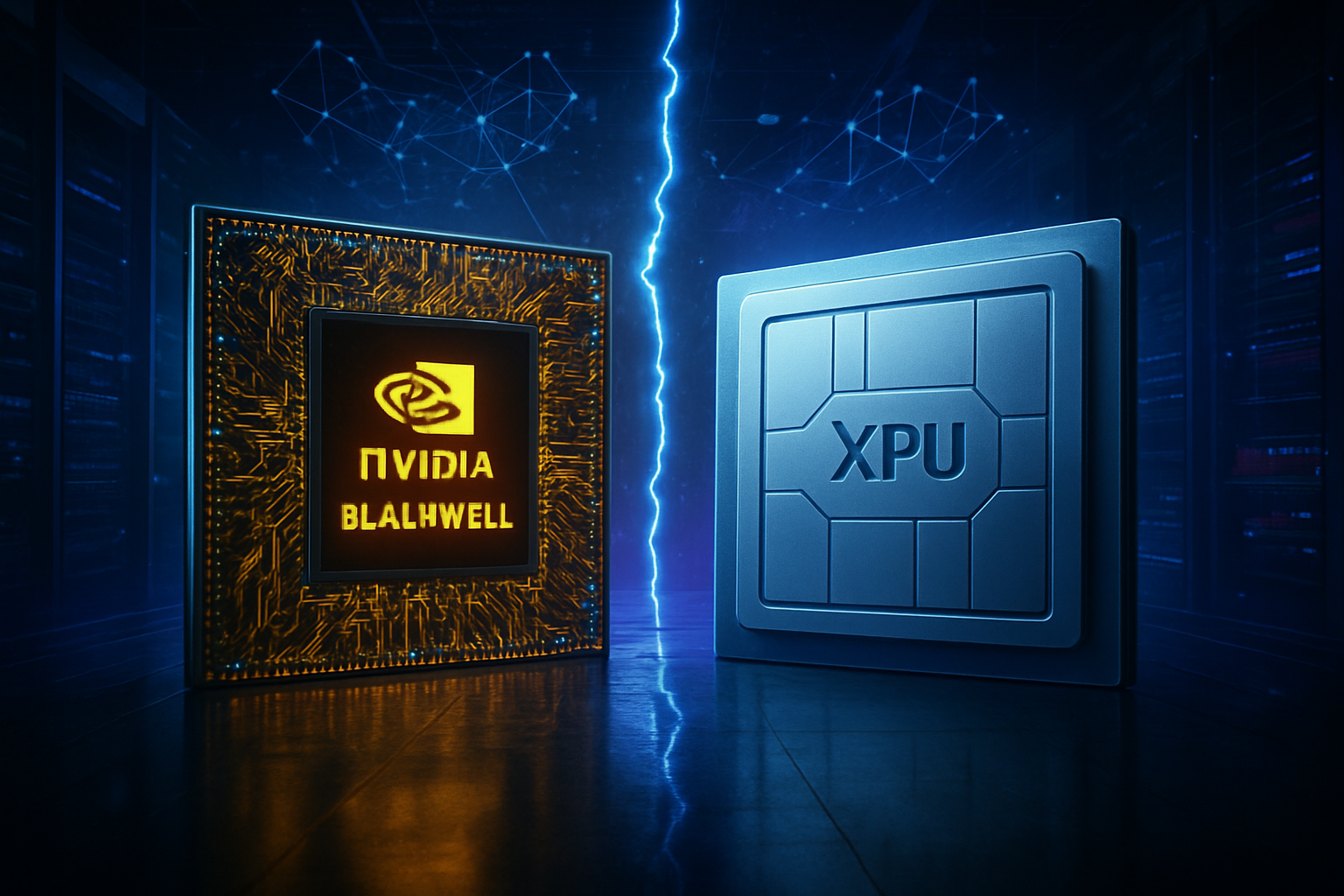
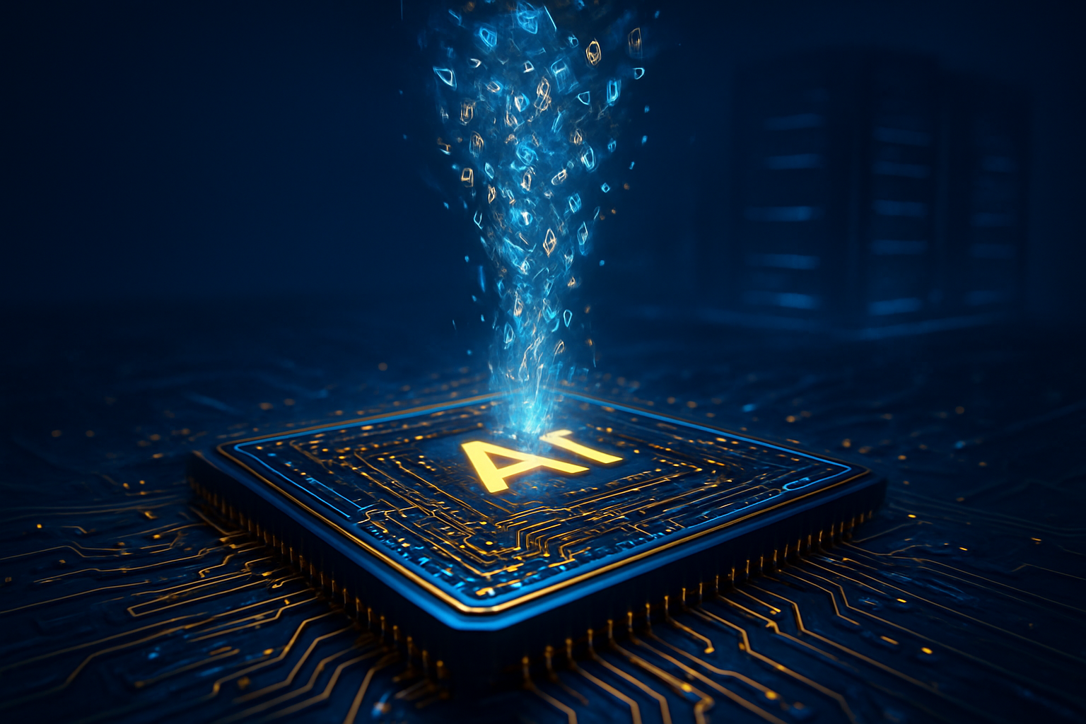
    The upcoming silicon, expected to see its first data center deployments in the second half of 2026, is not a direct clone of existing hardware. Instead, OpenAI and Broadcom (NASDAQ: AVGO) have developed a specialized inference engine tailored specifically for the "o1" series of reasoning models and future iterations of GPT. Unlike the general-purpose H100 or Blackwell chips from Nvidia (NASDAQ: NVDA), which are built to handle both the heavy lifting of training and the high-speed demands of inference, OpenAI’s chip is a "systolic array" design optimized for the dense matrix multiplications that define Transformer-based architectures.

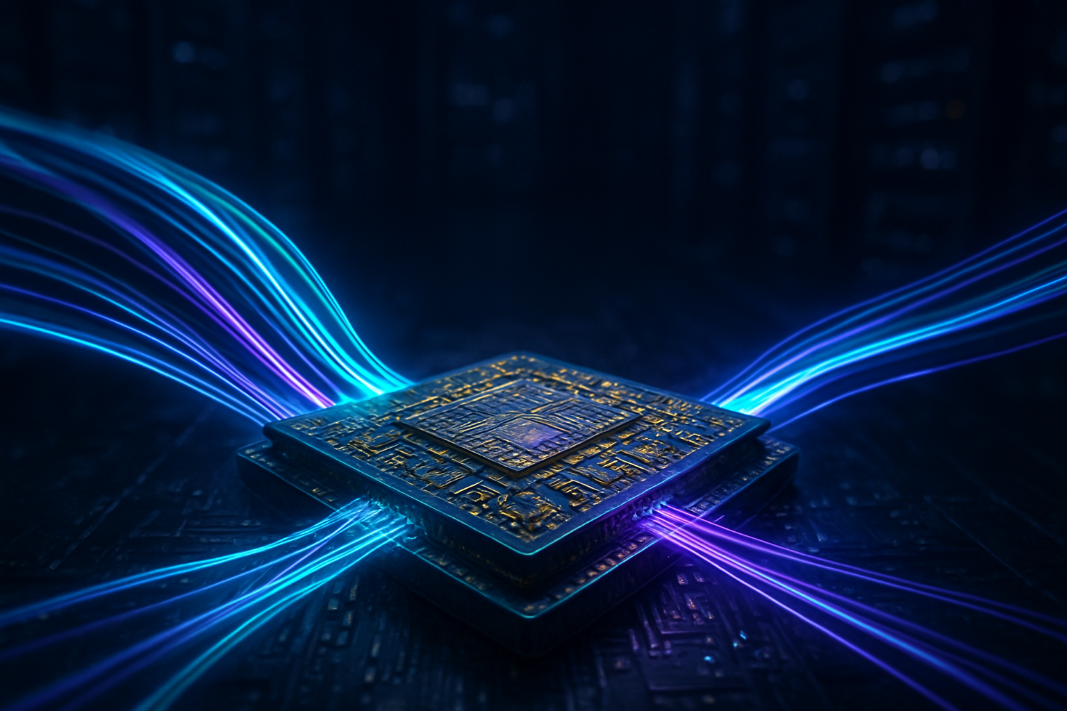
    Technical specifications confirmed by industry insiders suggest the chips will be fabricated using TSMC’s (NYSE: TSM) cutting-edge 3-nanometer (3nm) process. To ensure the chips can communicate at the scale required for 10 GW of power, Broadcom has integrated its industry-leading Ethernet-first networking architecture and high-speed PCIe interconnects directly into the chip's design. This "scale-out" capability is critical; it allows thousands of chips to act as a single, massive brain, reducing the latency that often plagues large-scale AI applications. Initial reactions from the AI research community have been overwhelmingly positive, with experts noting that this level of hardware-software co-design could lead to a 30% reduction in power consumption per token compared to current off-the-shelf solutions.

    Shifting the Power Dynamics of Silicon Valley

    The strategic implications for the tech industry are profound. For years, Nvidia (NASDAQ: NVDA) has enjoyed a near-monopoly on the high-end AI chip market, but OpenAI's move to custom silicon creates a blueprint for other AI labs to follow. While Nvidia remains the undisputed king of model training, OpenAI’s shift toward custom inference hardware targets the highest-volume part of the AI lifecycle. This development has sent ripples through the market, with analysts suggesting that the deal could generate upwards of $100 billion in revenue for Broadcom (NASDAQ: AVGO) through 2029, solidifying its position as the primary alternative for custom AI silicon.

    Furthermore, this move places OpenAI in a unique competitive position against other major tech players like Google (NASDAQ: GOOGL) and Amazon (NASDAQ: AMZN), who have long utilized their own custom TPUs and Trainium/Inferentia chips. By securing its own supply chain and manufacturing slots at TSMC, OpenAI is no longer solely dependent on the product cycles of external hardware vendors. This vertical integration provides a massive strategic advantage, allowing OpenAI to dictate its own scaling laws and potentially offer its API services at a price point that competitors reliant on expensive, general-purpose GPUs may find impossible to match.

    The 10 GW Vision and the "Transistors to Tokens" Philosophy

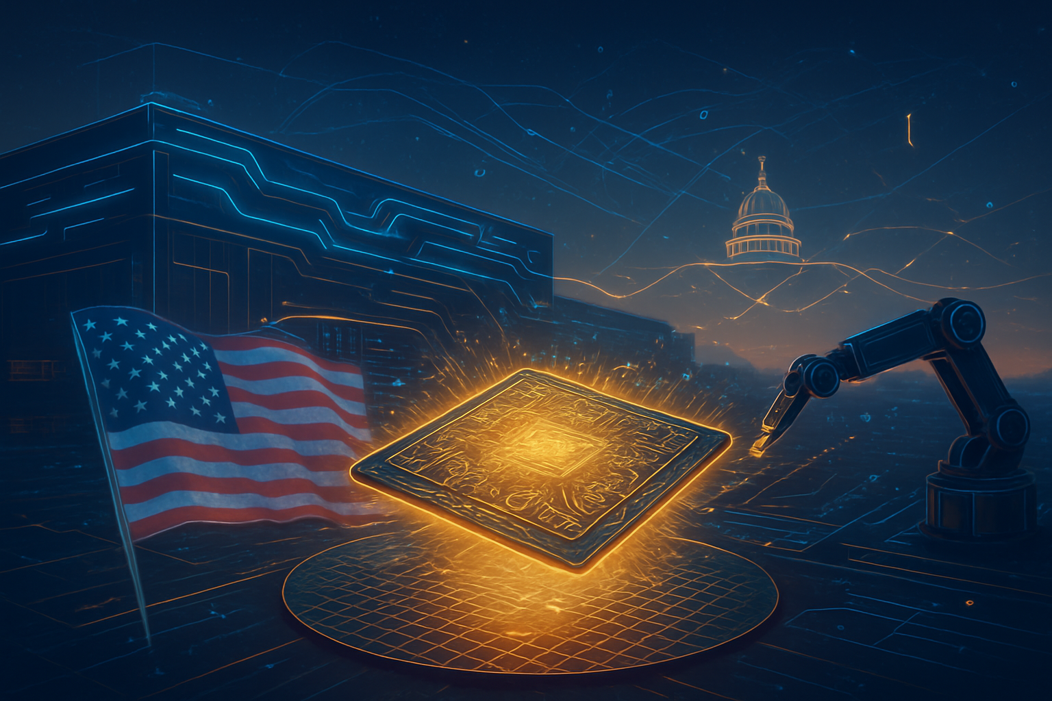
    At the heart of this project is CEO Sam Altman’s "transistors to tokens" philosophy. This vision treats the entire AI process as a single, unified pipeline. By controlling the silicon design, OpenAI can eliminate the overhead of features that are unnecessary for its specific models, maximizing "tokens per watt." This efficiency is not just an engineering goal; it is a necessity for the planned 10 GW deployment. To put that scale in perspective, 10 GW is enough power to support approximately 8 million homes, representing a fivefold increase in OpenAI’s current infrastructure footprint.

    This massive expansion is part of a broader trend where AI companies are becoming infrastructure and energy companies. The 10 GW plan includes the development of massive data center campuses, such as the rumored "Project Ludicrous," a 1.2 GW facility in Texas. The move toward such high-density power deployment has raised concerns about the environmental impact and the strain on the national power grid. However, OpenAI argues that the efficiency gains from custom silicon are the only way to make the massive energy demands of future "Super AI" models sustainable in the long term.

    The Road to 2026 and Beyond

    As we look toward 2026, the primary challenge for OpenAI and Broadcom (NASDAQ: AVGO) will be execution and manufacturing capacity. While the designs are finalized, the industry is currently facing a significant bottleneck in "CoWoS" (Chip-on-Wafer-on-Substrate) advanced packaging. OpenAI will be competing directly with Nvidia and Apple (NASDAQ: AAPL) for TSMC’s limited packaging capacity. Any delays in the supply chain could push the 2026 rollout into 2027, forcing OpenAI to continue relying on a mix of Nvidia’s Blackwell and AMD’s (NASDAQ: AMD) Instinct chips to bridge the gap.

    In the near term, we expect to see the first "tape-outs" of the silicon in early 2026, followed by rigorous testing in small-scale clusters. If successful, the deployment of these chips will likely coincide with the release of OpenAI’s next-generation "GPT-5" or "Sora" video models, which will require the massive throughput that only custom silicon can provide. Experts predict that if OpenAI can successfully navigate the transition to its own hardware, it will set a new standard for the industry, where the most successful AI companies are those that own the entire stack from the ground up.

    A New Chapter in AI History

    The finalization of the OpenAI-Broadcom partnership marks a historic turning point. It represents the moment when AI software evolved into a full-scale industrial infrastructure project. By taking control of its hardware destiny, OpenAI is attempting to ensure that the "intelligence" it produces remains economically viable as it scales to unprecedented levels. The transition from general-purpose computing to specialized AI silicon is no longer a theoretical goal—it is a multi-billion dollar reality with a clear deadline.

    As we move into 2026, the industry will be watching closely to see if the first physical chips live up to the "transistors to tokens" promise. The success of this project will likely determine the balance of power in the AI industry for the next decade. For now, the message is clear: the future of AI isn't just in the code—it's in the silicon.


    This content is intended for informational purposes only and represents analysis of current AI developments.

    TokenRing AI delivers enterprise-grade solutions for multi-agent AI workflow orchestration, AI-powered development tools, and seamless remote collaboration platforms.
    For more information, visit https://www.tokenring.ai/.

  • The Silicon Schism: NVIDIA’s Blackwell Faces a $50 Billion Custom Chip Insurgence

    The Silicon Schism: NVIDIA’s Blackwell Faces a $50 Billion Custom Chip Insurgence

    As 2025 draws to a close, the undisputed reign of NVIDIA (NASDAQ: NVDA) in the AI data center is facing its most significant structural challenge yet. While NVIDIA’s Blackwell architecture remains the gold standard for frontier model training, a parallel economy of "custom silicon" has reached a fever pitch. This week, industry reports and financial disclosures from Broadcom (NASDAQ: AVGO) have sent shockwaves through the semiconductor sector, revealing a staggering $50 billion pipeline for custom AI accelerators (XPUs) destined for the world’s largest hyperscalers.

    This shift represents a fundamental "Silicon Schism" in the AI industry. On one side stands NVIDIA’s general-purpose, high-margin GPU dominance, and on the other, a growing coalition of tech giants like Google (NASDAQ: GOOGL), Microsoft (NASDAQ: MSFT), and Meta (NASDAQ: META) who are increasingly designing their own chips to bypass the "NVIDIA tax." With Broadcom acting as the primary architect for these bespoke solutions, the competitive tension between the "Swiss Army Knife" of Blackwell and the "Precision Scalpels" of custom ASICs has become the defining battle of the generative AI era.

    The Technical Tug-of-War: Blackwell Ultra vs. The Rise of the XPU

    At the heart of this rivalry is the technical divergence between flexibility and efficiency. NVIDIA’s current flagship, the Blackwell Ultra (B300), which entered mass production in the second half of 2025, is a marvel of engineering. Boasting 288GB of HBM3E memory and delivering 15 PFLOPS of dense FP4 compute, it is designed to handle any AI workload thrown at it. However, this versatility comes at a cost—both in terms of power consumption and price. The Blackwell architecture is built to be everything to everyone, a necessity for researchers experimenting with new model architectures that haven't yet been standardized.

    In contrast, the custom Application-Specific Integrated Circuits (ASICs), or XPUs, being co-developed by Broadcom and hyperscalers, are stripped-down powerhouses. By late 2025, Google’s TPU v7 and Meta’s MTIA 3 have demonstrated that for specific, high-volume tasks—particularly inference and stable Transformer-based training—custom silicon can deliver up to a 50% improvement in power efficiency (TFLOPs per Watt) compared to Blackwell. These chips eliminate the "dark silicon" or unused features of a general-purpose GPU, focusing entirely on the tensor operations that drive modern Large Language Models (LLMs).

    Furthermore, the networking layer has become a critical technical battleground. NVIDIA relies on its proprietary NVLink interconnect to maintain its "moat," creating a tightly coupled ecosystem that is difficult to leave. Broadcom, however, has championed an open-standard approach, leveraging its Tomahawk 6 switching silicon to enable massive clusters of 1 million or more XPUs via high-performance Ethernet. This architectural split means that while NVIDIA offers a superior integrated "black box" solution, the custom XPU route offers hyperscalers the ability to scale their infrastructure horizontally with far more granular control over their thermal and budgetary envelopes.

    The $50 Billion Shift: Strategic Implications for Big Tech

    The financial gravity of this trend was underscored by Broadcom’s recent revelation of an AI-specific backlog exceeding $73 billion, with annual custom silicon revenue projected to hit $50 billion by 2026. This is not just a rounding error; it represents a massive redirection of capital expenditure (CapEx) away from NVIDIA. For companies like Google and Microsoft, the move to custom silicon is a strategic necessity to protect their margins. As AI moves from the "R&D phase" to the "deployment phase," the cost of running inference for billions of users makes the $35,000+ price tag of a Blackwell GPU increasingly untenable.

    The competitive implications are particularly stark for Broadcom, which has positioned itself as the "Kingmaker" of the custom silicon era. By providing the intellectual property and physical design services for chips like Google's TPU and Anthropic’s new $21 billion custom cluster, Broadcom is capturing the value that previously flowed almost exclusively to NVIDIA. This has created a bifurcated market: NVIDIA remains the essential partner for the most advanced "frontier" research—where the next generation of reasoning models is being birthed—while Broadcom and its partners are winning the war for "production-scale" AI.

    For startups and smaller AI labs, this development is a double-edged sword. While the rise of custom silicon may eventually lower the cost of cloud compute, these bespoke chips are currently reserved for the "Big Five" hyperscalers. This creates a potential "compute divide," where the owners of custom silicon enjoy a significantly lower Total Cost of Ownership (TCO) than those relying on public cloud instances of NVIDIA GPUs. As a result, we are seeing a trend where major model builders, such as Anthropic, are seeking direct partnerships with silicon designers to secure their own long-term hardware independence.

    A New Era of Efficiency: The Wider Significance of Custom Silicon

    The rise of custom ASICs marks a pivotal transition in the AI landscape, mirroring the historical evolution of other computing paradigms. Just as the early days of the internet saw a transition from general-purpose CPUs to specialized networking hardware, the AI industry is realizing that the sheer energy demands of Blackwell-class clusters are unsustainable. In a world where data center power is the ultimate constraint, a 40% reduction in TCO and power consumption—offered by custom XPUs—is not just a financial preference; it is a requirement for continued scaling.

    This shift also highlights the growing importance of the software compiler layer. One of NVIDIA’s strongest defenses has been CUDA, the software platform that has become the industry standard for AI development. However, the $50 billion investment in custom silicon is finally funding a viable alternative. Open-source initiatives like OpenAI’s Triton and Google’s OpenXLA are maturing, allowing developers to write code that can run on both NVIDIA GPUs and custom ASICs with minimal friction. As the software barrier to entry for custom silicon lowers, NVIDIA’s "software moat" begins to look less like a fortress and more like a hurdle.

    There are, however, concerns regarding the fragmentation of the AI hardware ecosystem. If every major hyperscaler develops its own proprietary chip, the "write once, run anywhere" dream of AI development could become more difficult. We are seeing a divergence where the "Inference Era" is dominated by specialized, efficient hardware, while the "Innovation Era" remains tethered to the flexibility of NVIDIA. This could lead to a two-tier AI economy, where the most efficient models are those locked behind the proprietary hardware of a few dominant cloud providers.

    The Road to Rubin: Future Developments and the Next Frontier

    Looking ahead to 2026, the battle is expected to intensify as NVIDIA prepares to launch its Rubin architecture (R100). Taped out on TSMC’s (NYSE: TSM) 3nm process, Rubin will feature HBM4 memory and a new 4x reticle chiplet design, aiming to reclaim the efficiency lead that custom ASICs have recently carved out. NVIDIA is also diversifying its own lineup, introducing "inference-first" GPUs like the Rubin CPX, which are designed to compete directly with custom XPUs on cost and power.

    On the custom side, the next horizon is the "10-gigawatt chip" project. Reports suggest that major players like OpenAI are working with Broadcom on massive, multi-year silicon roadmaps that integrate power management and liquid cooling directly into the chip architecture. These "AI Super-ASICs" will be designed not just for today’s Transformers, but for the "test-time scaling" and agentic workflows that are expected to dominate the AI landscape in 2026 and beyond.

    The ultimate challenge for both camps will be the physical limits of silicon. As we move toward 2nm and beyond, the gains from traditional Moore’s Law are diminishing. The next phase of competition will likely move beyond the chip itself and into the realm of "System-on-a-Wafer" and advanced 3D packaging. Experts predict that the winner of the next decade won't just be the company with the fastest chip, but the one that can most effectively manage the "Power-Performance-Area" (PPA) triad at a planetary scale.

    Summary: The Bifurcation of AI Compute

    The emergence of a $50 billion custom silicon market marks the end of the "GPU Monoculture." While NVIDIA’s Blackwell architecture remains a monumental achievement and the preferred tool for pushing the boundaries of what is possible, the economic and thermal realities of 2025 have forced a diversification of the hardware stack. Broadcom’s massive backlog and the aggressive chip roadmaps of Google, Microsoft, and Meta signal that the future of AI infrastructure is bespoke.

    In the coming months, the industry will be watching the initial benchmarks of the Blackwell Ultra against the first wave of 3nm custom XPUs. If the efficiency gap continues to widen, NVIDIA may find itself in the position of a high-end boutique—essential for the most complex tasks but increasingly bypassed for the high-volume work that powers the global AI economy. For now, the silicon war is far from over, but the era of the universal GPU is clearly being challenged by a new generation of precision-engineered silicon.


    This content is intended for informational purposes only and represents analysis of current AI developments.

    TokenRing AI delivers enterprise-grade solutions for multi-agent AI workflow orchestration, AI-powered development tools, and seamless remote collaboration platforms.
    For more information, visit https://www.tokenring.ai/.

  • The Backbone of AI: Broadcom Projects 150% AI Revenue Surge for FY2026 as Networking Dominance Solidifies

    The Backbone of AI: Broadcom Projects 150% AI Revenue Surge for FY2026 as Networking Dominance Solidifies

    In a move that has sent shockwaves through the semiconductor industry, Broadcom (NASDAQ: AVGO) has officially projected a staggering 150% year-over-year growth in AI-related revenue for fiscal year 2026. Following its December 2025 earnings update, the company revealed a massive $73 billion AI-specific backlog, positioning itself not merely as a component supplier, but as the indispensable architect of the global AI infrastructure. As hyperscalers race to build "mega-clusters" of unprecedented scale, Broadcom’s role in providing the high-speed networking and custom silicon required to glue these systems together has become the industry's most critical bottleneck.

    The significance of this announcement cannot be overstated. While much of the public's attention remains fixed on the GPUs that process AI data, Broadcom has quietly captured the market for the "fabric" that allows those GPUs to communicate. By guiding for AI semiconductor revenue to reach nearly $50 billion in FY2026—up from approximately $20 billion in 2025—Broadcom is signaling that the next phase of the AI revolution will be defined by connectivity and custom efficiency rather than raw compute alone.

    The Architecture of a Million-XPU Future

    At the heart of Broadcom’s growth is a suite of technical breakthroughs that address the most pressing challenge in AI today: scaling. As of late 2025, the company has begun shipping its Tomahawk 6 (codenamed "Davisson") and Jericho 4 platforms, which represent a generational leap in networking performance. The Tomahawk 6 is the world’s first 102.4 Tbps single-chip Ethernet switch, doubling the bandwidth of its predecessor and enabling the construction of clusters containing up to one million AI accelerators (XPUs). This "one million XPU" architecture is made possible by a two-tier "flat" network topology that eliminates the need for multiple layers of switches, reducing latency and complexity simultaneously.

    Technically, Broadcom is winning the war for the data center through Co-Packaged Optics (CPO). Traditionally, optical transceivers are separate modules that plug into the front of a switch, consuming massive amounts of power to move data across the circuit board. Broadcom’s CPO technology integrates the optical engines directly into the switch package. This shift reduces interconnect power consumption by as much as 70%, a critical factor as data centers hit the "power wall" where electricity availability, rather than chip availability, becomes the primary constraint on growth. Industry experts have noted that Broadcom’s move to a 3nm chiplet-based architecture for these switches allows for higher yields and better thermal management, further distancing them from competitors.

    The Custom Silicon Kingmaker

    Broadcom’s success is equally driven by its dominance in the custom ASIC (Application-Specific Integrated Circuit) market, which it refers to as its XPU business. The company has successfully transitioned from being a component vendor to a strategic partner for the world’s largest tech giants. Broadcom is the primary designer for Google’s (NASDAQ: GOOGL) TPU v5 and v6 chips and Meta’s (NASDAQ: META) MTIA accelerators. In late 2025, Broadcom confirmed that Anthropic has become its "fourth major customer," placing orders totaling $21 billion for custom AI racks.

    Speculation is also mounting regarding a fifth hyperscale customer, widely believed to be OpenAI or Microsoft (NASDAQ: MSFT), following reports of a $1 billion preliminary order for a custom AI silicon project. This shift toward custom silicon represents a direct challenge to the dominance of NVIDIA (NASDAQ: NVDA). While NVIDIA’s H100 and B200 chips are versatile, hyperscalers are increasingly turning to Broadcom to build chips tailored specifically for their own internal AI models, which can offer 3x to 5x better performance-per-watt for specific workloads. This strategic advantage allows tech giants to reduce their reliance on expensive, off-the-shelf GPUs while maintaining a competitive edge in model training speed.

    Solving the AI Power Crisis

    Beyond the raw performance metrics, Broadcom’s 2026 outlook is underpinned by its role in AI sustainability. As AI clusters scale toward 10-gigawatt power requirements, the inefficiency of traditional networking has become a liability. Broadcom’s Jericho 4 fabric router introduces "Geographic Load Balancing," allowing AI training jobs to be distributed across multiple data centers located hundreds of miles apart. This enables hyperscalers to utilize surplus renewable energy in different regions without the latency penalties that typically plague distributed computing.

    This development is a significant milestone in AI history, comparable to the transition from mainframe to cloud computing. By championing Scale-Up Ethernet (SUE), Broadcom is effectively democratizing high-performance AI networking. Unlike NVIDIA’s proprietary InfiniBand, which is a closed ecosystem, Broadcom’s Ethernet-based approach is open-source and interoperable. This has garnered strong support from the Open Compute Project (OCP) and has forced a shift in the market where Ethernet is now seen as a viable, and often superior, alternative for the largest AI training clusters in the world.

    The Road to 2027 and Beyond

    Looking ahead, Broadcom is already laying the groundwork for the next era of infrastructure. The company’s roadmap includes the transition to 1.6T and 3.2T networking ports by late 2026, alongside the first wave of 2nm custom AI accelerators. Analysts predict that as AI models continue to grow in size, the demand for Broadcom’s specialized SerDes (serializer/deserializer) technology will only intensify. The primary challenge remains the supply chain; while Broadcom has secured significant capacity at TSMC, the sheer volume of the $162 billion total consolidated backlog will require flawless execution to meet delivery timelines.

    Furthermore, the integration of VMware, which Broadcom acquired in late 2023, is beginning to pay dividends in the AI space. By layering VMware’s software-defined data center capabilities on top of its high-performance silicon, Broadcom is creating a full-stack "Private AI" offering. This allows enterprises to run sensitive AI workloads on-premises with the same efficiency as a hyperscale cloud, opening up a new multi-billion dollar market segment that has yet to be fully tapped.

    A New Era of Infrastructure Dominance

    Broadcom’s projected 150% AI revenue surge is a testament to the company's foresight in betting on Ethernet and custom silicon long before the current AI boom began. By positioning itself as the "backbone" of the industry, Broadcom has created a defensive moat that is difficult for any competitor to breach. While NVIDIA remains the face of the AI era, Broadcom has become its essential foundation, providing the plumbing that keeps the digital world's most advanced brains connected.

    As we move into 2026, investors and industry watchers should keep a close eye on the ramp-up of the fifth hyperscale customer and the first real-world deployments of Tomahawk 6. If Broadcom can successfully navigate the power and supply challenges ahead, it may well become the first networking-first company to join the multi-trillion dollar valuation club. For now, one thing is certain: the future of AI is being built on Broadcom silicon.


    This content is intended for informational purposes only and represents analysis of current AI developments.

    TokenRing AI delivers enterprise-grade solutions for multi-agent AI workflow orchestration, AI-powered development tools, and seamless remote collaboration platforms.
    For more information, visit https://www.tokenring.ai/.

  • The Silent King Ascends: Broadcom Surpasses $1 Trillion Milestone as the Backbone of AI

    The Silent King Ascends: Broadcom Surpasses $1 Trillion Milestone as the Backbone of AI

    In a historic shift for the global technology sector, Broadcom Inc. (NASDAQ: AVGO) has officially cemented its status as a titan of the artificial intelligence era, surpassing a $1 trillion market capitalization. While much of the public's attention has been captured by the meteoric rise of GPU manufacturers, Broadcom’s ascent signals a critical realization by the market: the AI revolution cannot happen without the complex "plumbing" and custom silicon that Broadcom uniquely provides. By late 2024 and throughout 2025, the company has transitioned from a diversified semiconductor conglomerate into the indispensable architect of the modern data center.

    This valuation milestone is not merely a reflection of stock market exuberance but a validation of Broadcom’s strategic pivot toward high-end AI infrastructure. As of December 22, 2025, the company’s market cap has stabilized in the $1.6 trillion to $1.7 trillion range, making it one of the most valuable entities on the planet. Broadcom now serves as the primary "Nvidia hedge" for hyperscalers, providing the networking fabric that allows tens of thousands of chips to work as a single cohesive unit and the custom design expertise that enables tech giants to build their own proprietary AI accelerators.

    The Architecture of Connectivity: Tomahawk 6 and the Networking Moat

    At the heart of Broadcom’s dominance is its networking silicon, specifically the Tomahawk and Jericho series, which have become the industry standard for AI clusters. In early 2025, Broadcom launched the Tomahawk 6, the world’s first single-chip 102.4 Tbps switch. This technical marvel is designed to solve the "interconnect bottleneck"—the phenomenon where AI training speeds are limited not by the raw power of individual GPUs, but by the speed at which data can move between them. The Tomahawk 6 enables the creation of "mega-clusters" comprising up to one million AI accelerators (XPUs) with ultra-low latency, a feat previously thought to be years away.

    Technically, Broadcom’s advantage lies in its commitment to the Ethernet standard. While NVIDIA Corporation (NASDAQ: NVDA) has historically pushed its proprietary InfiniBand technology for high-performance computing, Broadcom has successfully championed "AI-ready Ethernet." By integrating deep buffering and sophisticated load balancing into its Jericho 3-AI and Jericho 4 chips, Broadcom has eliminated packet loss—a critical requirement for AI training—while maintaining the interoperability and cost-efficiency of Ethernet. This shift has allowed hyperscalers to build open, flexible data centers that are not locked into a single vendor's ecosystem.

    Industry experts have noted that Broadcom’s networking moat is arguably deeper than that of any other semiconductor firm. Unlike software or even logic chips, the physical layer of high-speed networking requires decades of specialized IP and manufacturing expertise. The reaction from the research community has been one of profound respect for Broadcom’s ability to scale bandwidth at a rate that outpaces Moore’s Law, effectively providing the high-speed nervous system for the world's most advanced large language models.

    The Custom Silicon Powerhouse: From Google’s TPU to OpenAI’s Titan

    Beyond networking, Broadcom has established itself as the premier partner for Custom ASICs (Application-Specific Integrated Circuits). As hyperscalers seek to reduce their multi-billion dollar dependencies on general-purpose GPUs, they have turned to Broadcom to co-design bespoke AI silicon. This business segment has exploded in 2025, with Broadcom now managing the design and production of the world’s most successful custom chips. The partnership with Alphabet Inc. (NASDAQ: GOOGL) remains the gold standard, with Broadcom co-developing the TPU v7 on cutting-edge 3nm and 2nm processes, providing Google with a massive efficiency advantage in both training and inference.

    Meta Platforms, Inc. (NASDAQ: META) has also deepened its reliance on Broadcom for the Meta Training and Inference Accelerator (MTIA). The latest iterations of MTIA, ramping up in late 2025, offer up to a 50% improvement in energy efficiency for recommendation algorithms compared to standard hardware. Furthermore, the 2025 confirmation that OpenAI has tapped Broadcom for its "Titan" custom silicon project—a massive $10 billion engagement—has sent shockwaves through the industry. This move signals that even the most advanced AI labs are looking toward Broadcom to help them design the specialized hardware needed for frontier models like GPT-5 and beyond.

    This strategic positioning creates a "win-win" scenario for Broadcom. Whether a company buys Nvidia GPUs or builds its own custom chips, it almost inevitably requires Broadcom’s networking silicon to connect them. If a company decides to build its own chips to compete with Nvidia, it hires Broadcom to design them. This "king-maker" status has effectively insulated Broadcom from the competitive volatility of the AI chip race, leading many analysts to label it the "Silent King" of the infrastructure layer.

    The Nvidia Hedge: Broadcom’s Strategic Position in the AI Landscape

    Broadcom’s rise to a $1 trillion+ valuation represents a broader trend in the AI landscape: the maturation of the hardware stack. In the early days of the AI boom, the focus was almost entirely on the compute engine (the GPU). In 2025, the focus has shifted toward system-level efficiency and cost optimization. Broadcom sits at the intersection of these two needs. By providing the tools for hyperscalers to diversify their hardware, Broadcom acts as a critical counterbalance to Nvidia’s market dominance, offering a path toward a more competitive and sustainable AI ecosystem.

    This development has significant implications for the tech giants. For companies like Apple Inc. (NASDAQ: AAPL) and ByteDance, Broadcom provides the necessary IP to scale their internal AI initiatives without having to build a semiconductor division from scratch. However, this dominance also raises concerns about the concentration of power. With Broadcom controlling over 80% of the high-end Ethernet switching market, the company has become a single point of failure—or success—for the global AI build-out. Regulators have begun to take notice, though Broadcom’s business model of co-design and open standards has so far mitigated the antitrust concerns that have plagued more vertically integrated competitors.

    Comparatively, Broadcom’s milestone is being viewed as the "second phase" of the AI investment cycle. While Nvidia provided the initial spark, Broadcom is providing the long-term infrastructure. This mirrors previous tech cycles, such as the internet boom, where the companies building the routers and the fiber-optic standards eventually became as foundational as the companies building the personal computers.

    The Road to $2 Trillion: 2nm Processes and Global AI Expansion

    Looking ahead, Broadcom shows no signs of slowing down. The company is already deep into the development of 2nm-based custom silicon, which is expected to debut in late 2026. These next-generation chips will focus on extreme energy efficiency, addressing the growing power constraints that are currently limiting the size of data centers. Additionally, Broadcom is expanding its reach into "Sovereign AI," partnering with national governments to build localized AI infrastructure that is independent of the major US hyperscalers.

    Challenges remain, particularly in the integration of its massive VMware acquisition. While the software transition has been largely successful, the pressure to maintain high margins while scaling R&D for 2nm technology will be a significant test for CEO Hock Tan’s leadership. Furthermore, as AI workloads move increasingly to the "edge"—into phones and local devices—Broadcom will need to adapt its high-power data center expertise to more constrained environments. Experts predict that Broadcom’s next major growth engine will be the integration of optical interconnects directly into the chip package, a technology known as co-packaged optics (CPO), which could further solidify its networking lead.

    The Indispensable Infrastructure of the Intelligence Age

    Broadcom’s journey to a $1 trillion market capitalization is a testament to the company’s relentless focus on the most difficult, high-value problems in computing. By dominating the networking fabric and the custom silicon market, Broadcom has made itself indispensable to the AI revolution. It is the silent engine behind every Google search, every Meta recommendation, and every ChatGPT query.

    In the history of AI, 2025 will likely be remembered as the year the industry moved beyond the chip and toward the system. Broadcom’s success proves that in the gold rush of artificial intelligence, the most reliable profits are found not just in the gold itself, but in the sophisticated tools and transportation networks that make the entire economy possible. As we look toward 2026, the tech world will be watching Broadcom’s 2nm roadmap and its expanding ASIC pipeline as the definitive bellwether for the health of the global AI expansion.


    This content is intended for informational purposes only and represents analysis of current AI developments.

    TokenRing AI delivers enterprise-grade solutions for multi-agent AI workflow orchestration, AI-powered development tools, and seamless remote collaboration platforms.
    For more information, visit https://www.tokenring.ai/.

  • Silicon Sovereignty: How a Rumored TSMC Takeover Birthed the U.S. Government’s Equity Stake in Intel

    Silicon Sovereignty: How a Rumored TSMC Takeover Birthed the U.S. Government’s Equity Stake in Intel

    The global semiconductor landscape has undergone a transformation that few would have predicted eighteen months ago. What began as frantic rumors of a Taiwan Semiconductor Manufacturing Company (NYSE: TSM)-led consortium to rescue the struggling foundry assets of Intel Corporation (NASDAQ: INTC) has culminated in a landmark "Silicon Sovereignty" deal. This shift has effectively nationalized a portion of America’s leading chipmaker, with the U.S. government now holding a 9.9% non-voting equity stake in the company to ensure the goals of the CHIPS Act are not just met, but secured against geopolitical volatility.

    The rumors, which reached a fever pitch in the spring of 2025, suggested that TSMC was being courted by a "consortium of customers"—including NVIDIA (NASDAQ: NVDA), Advanced Micro Devices (NASDAQ: AMD), and Broadcom (NASDAQ: AVGO)—to take over the operational management of Intel’s manufacturing plants. While the joint venture never materialized in its rumored form, the threat of a foreign entity managing America’s most critical industrial assets forced a radical rethink of U.S. industrial policy. Today, on December 22, 2025, Intel stands as a stabilized "National Strategic Asset," having successfully entered high-volume manufacturing (HVM) for its 18A process node, a feat that marks the first time 2nm-class chips have been mass-produced on American soil.

    The Technical Turnaround: From 18A Rumors to High-Volume Reality

    The technical centerpiece of this saga is Intel’s 18A (1.8nm) process node. Throughout late 2024 and early 2025, the industry was rife with skepticism regarding Intel’s ability to deliver on its "five nodes in four years" roadmap. Critics argued that the complexity of RibbonFET gate-all-around (GAA) transistors and PowerVia backside power delivery—technologies essential for the 18A node—were beyond Intel’s reach without external intervention. The rumored TSMC-led joint venture was seen as a way to inject "Taiwanese operational discipline" into Intel’s fabs to save these technologies from failure.

    However, under the leadership of CEO Lip-Bu Tan, who took the helm in March 2025 following the ousting of Pat Gelsinger, Intel focused its depleted resources exclusively on the 18A ramp-up. The technical specifications of 18A are formidable: it offers a 10% improvement in performance-per-watt over its predecessor and introduces a level of transistor density that rivals TSMC’s N2 node. By December 19, 2025, Intel’s Arizona and Ohio fabs officially moved into HVM, supported by the first commercial installations of High-NA EUV lithography machines.

    This achievement differs from previous Intel efforts by decoupling the design and manufacturing arms more aggressively. The initial reactions from the research community have been cautiously optimistic. Experts note that while Intel 18A is technically competitive, the real breakthrough was the implementation of a "copy-exactly" manufacturing philosophy—a hallmark of TSMC—which Intel finally adopted at scale in 2025. This move was facilitated by a $3.2 billion "Secure Enclave" grant from the Department of Defense, which provided the financial buffer necessary to perfect the 18A yields.

    A Consortium of Necessity: Impact on Tech Giants and Competitors

    The rumored involvement of NVIDIA, AMD, and Broadcom in a potential Intel Foundry takeover was driven by a desperate need for supply chain diversification. Throughout 2024, these companies were almost entirely dependent on TSMC’s facilities in Taiwan, creating a "single point of failure" for the AI revolution. While the TSMC-led joint venture was officially denied by CEO C.C. Wei in September 2025, the underlying pressure led to a different kind of alliance: the "Equity for Subsidies" model.

    NVIDIA and SoftBank (OTC: SFTBY) have since emerged as major strategic investors, contributing $5 billion and $2 billion respectively to Intel’s foundry expansion. For NVIDIA, this investment serves as an insurance policy. By helping Intel succeed, NVIDIA ensures it has a secondary source for its next-generation Blackwell and Rubin GPUs, reducing its reliance on the Taiwan Strait. AMD and Broadcom, while not direct equity investors, have signed multi-year "anchor customer" agreements, committing to shift a portion of their sub-5nm production to Intel’s U.S.-based fabs by 2027.

    This development has disrupted the market positioning of pure-play foundries. Samsung’s foundry division has struggled to keep pace, leaving Intel as the only viable domestic alternative to TSMC. The strategic advantage for U.S. tech giants is clear: they now have a "home court" advantage in manufacturing, which mitigates the risk of export controls or regional conflicts disrupting their hardware pipelines.

    De-risking the CHIPS Act and the Rise of Silicon Sovereignty

    The broader significance of the Intel rescue cannot be overstated. It represents the end of the "hands-off" era of American industrial policy. The U.S. government’s decision to convert $8.9 billion in CHIPS Act grants into a 9.9% equity stake—a move dubbed "Silicon Sovereignty"—was a direct response to the risk that Intel might be broken up or sold to foreign interests. This "Golden Share" gives the White House veto power over any future sale or spin-off of Intel’s foundry business for the next five years.

    This fits into a global trend of "de-risking" where nations are treating semiconductor manufacturing with the same strategic gravity as oil reserves or nuclear energy. By taking an equity stake, the U.S. government has effectively "de-risked" the massive capital expenditure required for Intel’s $89.6 billion fab expansion. This model is being compared to the 2009 automotive bailouts, but with a futuristic twist: the government is not just saving jobs, it is securing the foundational technology of the AI era.

    However, this intervention has raised concerns about market competition and the potential for political interference in corporate strategy. Critics argue that by picking a "national champion," the U.S. may stifle smaller innovators. Yet, compared to previous milestones like the invention of the transistor or the rise of the PC, the 2025 stabilization of Intel marks a shift from a globalized, borderless tech industry to one defined by regional blocs and national security imperatives.

    The Horizon: 14A, High-NA EUV, and the Next Frontier

    Looking ahead, the next 24 months will be defined by Intel’s transition to the 14A (1.4nm) node. Expected to enter risk production in late 2026, 14A will be the first node to fully utilize High-NA EUV at scale across multiple layers. The challenge remains daunting: Intel must prove that it can not only manufacture these chips but do so profitably. The foundry division remains loss-making as of December 2025, though the losses have stabilized significantly compared to the disastrous 2024 fiscal year.

    Future applications for this domestic capacity include a new generation of "Sovereign AI" chips—hardware designed specifically for government and defense applications that never leaves U.S. soil during the fabrication process. Experts predict that if Intel can maintain its 18A yields through 2026, it will begin to win back significant market share from TSMC, particularly for high-performance computing (HPC) and automotive applications where supply chain security is paramount.

    Conclusion: A New Chapter for American Silicon

    The saga of the TSMC-Intel rumors and the subsequent government intervention marks a turning point in the history of technology. The key takeaway is that the "too big to fail" doctrine has officially arrived in Silicon Valley. Intel’s survival was deemed so critical to the U.S. economy and national security that the government was willing to abandon decades of neoliberal economic policy to become a shareholder.

    As we move into 2026, the significance of this development will be measured by the stability of the AI supply chain. The "Silicon Sovereignty" deal has provided a roadmap for how other Western nations might protect their own critical tech sectors. For now, the industry will be watching Intel’s quarterly yield reports and the progress of its Ohio "mega-fab" with intense scrutiny. The rumors of a TSMC takeover may have faded, but the transformation they sparked has permanently altered the geography of the digital world.


    This content is intended for informational purposes only and represents analysis of current AI developments.

    TokenRing AI delivers enterprise-grade solutions for multi-agent AI workflow orchestration, AI-powered development tools, and seamless remote collaboration platforms.
    For more information, visit https://www.tokenring.ai/.

  • Beyond the Green Giant: The Architects Building the AI Infrastructure Frontier

    Beyond the Green Giant: The Architects Building the AI Infrastructure Frontier

    The artificial intelligence revolution has long been synonymous with a single name, but as of December 19, 2025, the narrative of a "one-company monopoly" has officially fractured. While Nvidia remains a titan of the industry, the bedrock of the AI era is being reinforced by a diverse coalition of hardware and software innovators. From custom silicon designed in-house by hyperscalers to the rapid maturation of open-source software stacks, the infrastructure layer is undergoing its most significant transformation since the dawn of deep learning.

    This shift represents a strategic pivot for the entire tech sector. As the demand for massive-scale inference and training continues to outpace supply, the industry has moved toward a multi-vendor ecosystem. This diversification is not just about cost—it is about architectural sovereignty, energy efficiency, and breaking the "software moat" that once locked developers into a single proprietary ecosystem.

    The Technical Vanguard: AMD and Intel’s High-Stakes Counteroffensive

    The technical battleground in late 2025 is defined by memory density and compute efficiency. Advanced Micro Devices (NASDAQ:AMD) has successfully executed its aggressive annual roadmap, culminating in the volume production of the Instinct MI355X. Built on a cutting-edge 3nm process, the MI355X features a staggering 288GB of HBM3E memory. This capacity allows for the local hosting of increasingly massive large language models (LLMs) that previously required complex splitting across multiple nodes. By introducing support for FP4 and FP6 data types, AMD has claimed a 35-fold increase in inference performance over its previous generations, directly challenging the dominance of Nvidia’s Blackwell architecture in the enterprise data center.

    Intel Corporation (NASDAQ:INTC) has similarly pivoted its strategy, moving beyond the standalone Gaudi 3 accelerator to its unified "Falcon Shores" architecture. Falcon Shores represents a technical milestone for Intel, merging the high-performance AI capabilities of the Gaudi line with the versatile Xe-HPC graphics technology. This "XPU" approach is designed to provide a 5x improvement in performance-per-watt, addressing the critical energy constraints facing modern data centers. Furthermore, Intel’s oneAPI 2025.1 toolkit has become a vital bridge for developers, offering a streamlined path for migrating legacy CUDA code to open standards, effectively lowering the barrier to entry for non-Nvidia hardware.

    The technical evolution extends into the very fabric of the data center. The Ultra Ethernet Consortium (UEC), which released its 1.0 Specification in June 2025, has introduced a standardized alternative to proprietary interconnects like InfiniBand. By optimizing Ethernet for AI workloads through advanced congestion control and packet-spraying techniques, the UEC has enabled companies like Arista Networks, Inc. (NYSE:ANET) and Cisco Systems, Inc. (NASDAQ:CSCO) to deploy massive "AI back-end" fabrics. These networks support the 800G and 1.6T speeds necessary for the next generation of multi-trillion parameter models, ensuring that the network is no longer a bottleneck for distributed training.

    The Hyperscaler Rebellion: Custom Silicon and the ASIC Boom

    The most profound shift in the market positioning of AI infrastructure comes from the "Hyperscaler Rebellion." Alphabet Inc. (NASDAQ:GOOGL), Amazon.com, Inc. (NASDAQ:AMZN), and Meta have increasingly bypassed general-purpose GPUs in favor of custom Application-Specific Integrated Circuits (ASICs). Broadcom Inc. (NASDAQ:AVGO) has emerged as the primary architect of this movement, co-developing Google’s TPU v6 (Trillium) and Meta’s Training and Inference Accelerator (MTIA). These custom chips are hyper-optimized for specific workloads, such as recommendation engines and transformer-based inference, providing a performance-per-dollar ratio that general-purpose silicon struggle to match.

    This move toward custom silicon has created a lucrative niche for Marvell Technology, Inc. (NASDAQ:MRVL), which has partnered with Microsoft Corporation (NASDAQ:MSFT) on the Maia chip series and Amazon on the Trainium 2 and 3 programs. For these tech giants, the strategic advantage is two-fold: it reduces their multi-billion dollar dependency on external vendors and allows them to tailor their hardware to the specific nuances of their proprietary models. As of late 2025, custom ASICs now account for nearly 30% of the total AI compute deployed in the world's largest data centers, a significant jump from just two years ago.

    The competitive implications are stark. For startups and mid-tier AI labs, the availability of diverse hardware means lower cloud compute costs and more options for scaling. The "software moat" once provided by Nvidia’s CUDA has been eroded by the maturation of open-source projects like PyTorch and AMD’s ROCm 7.0. These software layers now provide "day-zero" support for new hardware, allowing researchers to switch between different GPU and TPU clusters with minimal code changes. This interoperability has leveled the playing field, fostering a more competitive and resilient market.

    A Multi-Polar AI Landscape: Resilience and Standardization

    The wider significance of this diversification cannot be overstated. In the early 2020s, the AI industry faced a "compute crunch" that threatened to stall innovation. By 12/19/2025, the rise of a multi-polar infrastructure landscape has mitigated these supply chain risks. The reliance on a single vendor’s production cycle has been replaced by a distributed supply chain involving multiple foundries and assembly partners. This resilience is critical as AI becomes integrated into essential global infrastructure, from healthcare diagnostics to autonomous energy grids.

    Standardization has become the watchword of 2025. The success of the Ultra Ethernet Consortium and the widespread adoption of the OCP (Open Compute Project) standards for server design have turned AI infrastructure into a modular ecosystem. This mirrors the evolution of the early internet, where proprietary protocols eventually gave way to the open standards that enabled global scale. By decoupling the hardware from the software, the industry has ensured that the "AI boom" is not a bubble tied to the fortunes of a single firm, but a sustainable technological era.

    However, this transition is not without its concerns. The rapid proliferation of high-power chips from multiple vendors has placed an unprecedented strain on the global power grid. Companies are now competing not just for chips, but for access to "power-dense" data center sites. This has led to a surge in investment in modular nuclear reactors and advanced liquid cooling technologies. The comparison to previous milestones, such as the transition from mainframes to client-server architecture, is apt: we are seeing the birth of a new utility-grade compute layer that will define the next century of economic activity.

    The Horizon: 1.6T Networking and the Road to 2nm

    Looking ahead to 2026 and beyond, the focus will shift toward even tighter integration between compute and memory. Industry leaders are already testing "3D-stacked" logic and memory configurations, with Micron Technology, Inc. (NASDAQ:MU) playing a pivotal role in delivering the next generation of HBM4 memory. These advancements will be necessary to support the "Agentic AI" revolution, where thousands of autonomous agents operate simultaneously, requiring massive, low-latency inference capabilities.

    Furthermore, the transition to 2nm process nodes is expected to begin in late 2026, promising another leap in efficiency. Experts predict that the next major challenge will be "optical interconnects"—using light instead of electricity to move data between chips. This would virtually eliminate the latency and heat issues that currently plague large-scale AI clusters. As these technologies move from the lab to the data center, we can expect a new wave of applications, including real-time, high-fidelity holographic communication and truly global, decentralized AI networks.

    Conclusion: A New Era of Infrastructure

    The AI infrastructure landscape of late 2025 is a testament to the industry's ability to adapt and scale. The emergence of AMD, Intel, Broadcom, and Marvell as critical pillars alongside Nvidia has created a robust, competitive environment that benefits the entire ecosystem. From the custom silicon powering the world's largest clouds to the open-source software stacks that democratize access to compute, the "shovels" of the AI gold rush are more diverse and powerful than ever before.

    As we look toward the coming months, the key metric to watch will be the "utilization-to-cost" ratio of these new platforms. The success of the multi-vendor era will be measured by how effectively it can lower the cost of intelligence, making advanced AI accessible not just to tech giants, but to every enterprise and developer on the planet. The foundation has been laid; the era of multi-polar AI infrastructure has arrived.


    This content is intended for informational purposes only and represents analysis of current AI developments.

    TokenRing AI delivers enterprise-grade solutions for multi-agent AI workflow orchestration, AI-powered development tools, and seamless remote collaboration platforms.
    For more information, visit https://www.tokenring.ai/.

  • The Trillion-Dollar Nexus: OpenAI’s Funding Surge and the Race for Global AI Sovereignty

    The Trillion-Dollar Nexus: OpenAI’s Funding Surge and the Race for Global AI Sovereignty

    SAN FRANCISCO — December 18, 2025 — OpenAI is currently navigating a transformative period that is reshaping the global technology landscape, as the company enters the final stages of a historic $100 billion funding round. This massive capital injection, which values the AI pioneer at a staggering $750 billion, is not merely a play for software dominance but the cornerstone of a radical shift toward vertical integration. By securing unprecedented levels of investment from entities like SoftBank Group Corp. (OTC:SFTBY), Thrive Capital, and a strategic $10 billion-plus commitment from Amazon.com, Inc. (NASDAQ:AMZN), OpenAI is positioning itself to bridge the "electron gap" and the chronic shortage of high-performance semiconductors that have defined the AI era.

    The immediate significance of this development lies in the decoupling of OpenAI from its total reliance on merchant silicon. While the company remains a primary customer of NVIDIA Corporation (NASDAQ:NVDA), this new funding is being funneled into "Stargate LLC," a multi-national joint venture designed to build "gigawatt-scale" data centers and proprietary AI chips. This move signals the end of the "software-only" era for AI labs, as Sam Altman’s vision for AI infrastructure begins to dictate the roadmap for the entire semiconductor industry, forcing a realignment of global supply chains and energy policies.

    The Architecture of "Stargate": Custom Silicon and Gigawatt-Scale Compute

    At the heart of OpenAI’s infrastructure push is a custom Application-Specific Integrated Circuit (ASIC) co-developed with Broadcom Inc. (NASDAQ:AVGO). Unlike the general-purpose power of NVIDIA’s upcoming Rubin architecture, the OpenAI-Broadcom chip is a "bespoke" inference engine built on Taiwan Semiconductor Manufacturing Company’s (NYSE:TSM) 3nm process. Technical specifications reveal a systolic array design optimized for the dense matrix multiplications inherent in Transformer-based models like the recently teased "o2" reasoning engine. By stripping away the flexibility required for non-AI workloads, OpenAI aims to reduce the power consumption per token by an estimated 30% compared to off-the-shelf hardware.

    The physical manifestation of this vision is "Project Ludicrous," a 1.2-gigawatt data center currently under construction in Abilene, Texas. This site is the first of many planned under the Stargate LLC umbrella, a partnership that now includes Oracle Corporation (NYSE:ORCL) and the Abu Dhabi-backed MGX. These facilities are being designed with liquid-cooling at their core to handle the 1,800W thermal design power (TDP) of modern AI racks. Initial reactions from the research community have been a mix of awe and concern; while the scale promises a leap toward Artificial General Intelligence (AGI), experts warn that the sheer concentration of compute power in a single entity’s hands creates a "compute moat" that may be insurmountable for smaller rivals.

    A New Semiconductor Order: Winners, Losers, and Strategic Pivots

    The ripple effects of OpenAI’s funding and infrastructure plans are being felt across the "Magnificent Seven" and the broader semiconductor market. Broadcom has emerged as a primary beneficiary, now controlling nearly 89% of the custom AI ASIC market as it helps OpenAI, Meta Platforms, Inc. (NASDAQ:META), and Alphabet Inc. (NASDAQ:GOOGL) design their own silicon. Meanwhile, NVIDIA has responded to the threat of custom chips by accelerating its product cycle to a yearly cadence, moving from Blackwell to the Rubin (R100) platform in record time to maintain its performance lead in training-heavy workloads.

    For tech giants like Amazon and Microsoft Corporation (NASDAQ:MSFT), the relationship with OpenAI has become increasingly complex. Amazon’s $10 billion investment is reportedly tied to OpenAI’s adoption of Amazon’s Trainium chips, a strategic move by the e-commerce giant to ensure its own silicon finds a home in the world’s most advanced AI models. Conversely, Microsoft, while still a primary partner, is seeing OpenAI diversify its infrastructure through Stargate LLC to avoid vendor lock-in. This "multi-vendor" strategy has also provided a lifeline to Advanced Micro Devices, Inc. (NASDAQ:AMD), whose MI300X and MI350 series chips are being used as critical bridging hardware until OpenAI’s custom silicon reaches mass production in late 2026.

    The Electron Gap and the Geopolitics of Intelligence

    Beyond the chips themselves, Sam Altman’s vision has highlighted a looming crisis in the AI landscape: the "electron gap." As OpenAI aims for 100 GW of new energy capacity per year to fuel its scaling laws, the company has successfully lobbied the U.S. government to treat AI infrastructure as a national security priority. This has led to a resurgence in nuclear energy investment, with startups like Oklo Inc. (NYSE:OKLO)—where Altman serves as chairman—breaking ground on fission sites to power the next generation of data centers. The transition to a Public Benefit Corporation (PBC) in October 2025 was a key prerequisite for this, allowing OpenAI to raise the trillions needed for energy and foundries without the constraints of a traditional profit cap.

    This massive scaling effort is being compared to the Manhattan Project or the Apollo program in its scope and national significance. However, it also raises profound environmental and social concerns. The 10 GW of power OpenAI plans to consume by 2029 is equivalent to the energy usage of several small nations, leading to intense scrutiny over the carbon footprint of "reasoning" models. Furthermore, the push for "Sovereign AI" has sparked a global arms race, with the UK, UAE, and Australia signing deals for their own Stargate-class data centers to ensure they are not left behind in the transition to an AI-driven economy.

    The Road to 2026: What Lies Ahead for AI Infrastructure

    Looking toward 2026, the industry expects the first "silicon-validated" results from the OpenAI-Broadcom partnership. If these custom chips deliver the promised efficiency gains, it could lead to a permanent shift in how AI is monetized, significantly lowering the "cost-per-query" and enabling widespread integration of high-reasoning agents in consumer devices. However, the path is fraught with challenges, most notably the advanced packaging bottleneck at TSMC. The global supply of CoWoS (Chip-on-Wafer-on-Substrate) remains the single greatest constraint on OpenAI’s ambitions, and any geopolitical instability in the Taiwan Strait could derail the entire $1.4 trillion infrastructure plan.

    In the near term, the AI community is watching for the official launch of GPT-5, which is expected to be the first model trained on a cluster of over 100,000 H100/B200 equivalents. Analysts predict that the success of this model will determine whether the massive capital expenditures of 2025 were a visionary investment or a historic overreach. As OpenAI prepares for a potential IPO in late 2026, the focus will shift from "how many chips can they buy" to "how efficiently can they run the chips they have."

    Conclusion: The Dawn of the Infrastructure Era

    The ongoing funding talks and infrastructure maneuvers of late 2025 mark a definitive turning point in the history of artificial intelligence. OpenAI is no longer just an AI lab; it is becoming a foundational utility company for the cognitive age. By integrating chip design, energy production, and model development, Sam Altman is attempting to build a vertically integrated empire that rivals the industrial titans of the 20th century. The significance of this development cannot be overstated—it represents a bet that the future of the global economy will be written in silicon and powered by nuclear-backed data centers.

    As we move into 2026, the key metrics to watch will be the progress of "Project Ludicrous" in Texas and the stability of the burgeoning partnership between OpenAI and the semiconductor giants. Whether this trillion-dollar gamble leads to the realization of AGI or serves as a cautionary tale of "compute-maximalism," one thing is certain: the relationship between AI funding and hardware demand has fundamentally altered the trajectory of the tech industry.


    This content is intended for informational purposes only and represents analysis of current AI developments.

    TokenRing AI delivers enterprise-grade solutions for multi-agent AI workflow orchestration, AI-powered development tools, and seamless remote collaboration platforms.
    For more information, visit https://www.tokenring.ai/.

  • Broadcom’s 20% AI Correction: Why the ‘Plumbing of the Internet’ Just Hit a Major Speed Bump

    Broadcom’s 20% AI Correction: Why the ‘Plumbing of the Internet’ Just Hit a Major Speed Bump

    As of December 18, 2025, the semiconductor landscape is grappling with a paradox: Broadcom Inc. (NASDAQ: AVGO) is reporting record-breaking demand for its artificial intelligence infrastructure, yet its stock has plummeted more than 20% from its December 9 all-time high of $414.61. This sharp correction, which has seen shares retreat to the $330 range in just over a week, has sent shockwaves through the tech sector. While the company’s Q4 fiscal 2025 earnings beat expectations, a confluence of "margin anxiety," a "sell the news" reaction to a massive OpenAI partnership, and broader valuation concerns have triggered a significant reset for the networking giant.

    The immediate significance of this dip lies in the growing tension between Broadcom’s market-share dominance and its shifting profitability profile. As the primary provider of custom AI accelerators (XPUs) and high-end Ethernet switching for hyperscalers like Google (NASDAQ: GOOGL) and Meta Platforms, Inc. (NASDAQ: META), Broadcom is the undisputed "plumbing" of the AI revolution. However, the transition from selling high-margin individual chips to complex, integrated system-level solutions has introduced a new variable: margin compression. Investors are now forced to decide if the current 21% discount represents a generational entry point or the first crack in the "AI infrastructure supercycle."

    The Technical Engine: Tomahawk 6 and the Custom Silicon Pivot

    The technical catalyst behind Broadcom's current market position—and its recent volatility—is the aggressive rollout of its next-generation networking stack. In late 2025, Broadcom began volume shipping the Tomahawk 6 (TH6-Davisson), the world’s first 102.4 Tbps Ethernet switch. This chip doubles the bandwidth of its predecessor and, for the first time, widely implements Co-Packaged Optics (CPO). By integrating optical components directly onto the silicon package, Broadcom has managed to slash power consumption in 100,000+ GPU clusters—a critical requirement as data centers hit the "power wall."

    Beyond networking, Broadcom’s custom ASIC (Application-Specific Integrated Circuit) business has become its primary growth engine. The company now holds an estimated 89% market share in this space, co-developing "XPUs" that are optimized for specific AI workloads. Unlike general-purpose GPUs from NVIDIA Corporation (NASDAQ: NVDA), these custom chips are architected for maximum efficiency in inference—the process of running AI models. The recent technical milestone of the Ultra Ethernet Consortium (UEC) 1.0 specification has further empowered Broadcom, allowing its Ethernet fabric to achieve sub-2ms latency, effectively neutralizing the performance advantage previously held by Nvidia’s proprietary InfiniBand interconnect.

    However, these technical triumphs come with a financial caveat. To win the "inference war," Broadcom has moved toward delivering full-rack solutions that include lower-margin third-party components like High Bandwidth Memory (HBM4). This shift led to management's guidance of a 100-basis-point gross margin compression for early 2026. While the technical community views the move to integrated systems as a brilliant strategic "lock-in" play, the financial community reacted with "margin jitters," viewing the dip in percentage points as a potential sign of waning pricing power.

    The Hyperscale Impact: OpenAI, Meta, and the 'Nvidia Tax'

    The ripple effects of Broadcom’s stock dip are being felt across the "Magnificent Seven" and the broader AI lab ecosystem. The most significant development of late 2025 was the confirmation of a landmark 10-gigawatt (GW) deal with OpenAI. This multi-year partnership aims to co-develop custom accelerators and networking for OpenAI’s future AGI-class models. While the deal is projected to yield up to $150 billion in revenue through 2029, the market’s "sell the news" reaction suggests that investors are weary of the long lead times—meaningful revenue from the OpenAI deal isn't expected to hit the balance sheet until 2027.

    For competitors like Marvell Technology, Inc. (NASDAQ: MRVL), Broadcom’s dip is a double-edged sword. While Marvell is growing faster from a smaller base, Broadcom’s scale remains a massive barrier to entry. Broadcom’s current AI backlog stands at a staggering $73 billion, nearly ten times Marvell's total annual revenue. This backlog provides a safety net for Broadcom, even as its stock price wavers. By providing a credible, open-standard alternative to Nvidia’s vertically integrated "walled garden," Broadcom has become the preferred partner for tech giants looking to avoid the "Nvidia tax"—the high premium and supply constraints associated with the H200 and Blackwell series.

    The strategic advantage for companies like Google and Meta is clear: by using Broadcom’s custom silicon, they can optimize hardware for their specific software stacks (like Google’s TPU v7), resulting in a lower "cost per token." This efficiency is becoming the primary metric for success as the industry shifts from training massive models to serving them to billions of users at scale.

    Wider Significance: The Great Networking War and the AI Landscape

    Broadcom’s 20% correction marks a pivotal moment in the broader AI landscape, signaling a shift from speculative hype to "execution reality." For the past two years, the market has rewarded any company associated with AI infrastructure with sky-high valuations. Broadcom’s peak 42x forward earnings multiple was a testament to this optimism. However, the mid-December 2025 correction suggests that the market is beginning to differentiate between "growth at any cost" and "sustainable margin growth."

    A major trend highlighted by this event is the definitive victory of Ethernet over InfiniBand for large-scale AI inference. As clusters grow toward the "one million XPU" mark, the economics of proprietary networking like Nvidia’s InfiniBand become untenable. Broadcom’s push for open standards via the Ultra Ethernet Consortium has successfully commoditized high-performance networking, making it accessible to a wider range of players. This democratization of high-speed interconnects is essential for the next phase of AI development, where smaller labs and startups will need to compete with the compute-rich giants.

    Furthermore, Broadcom’s situation mirrors previous tech milestones, such as the transition from mainframe to client-server or the early days of cloud infrastructure. In each case, the "plumbing" providers initially saw margin compression as they scaled, only to emerge as high-margin monopolies once the infrastructure became indispensable. Industry experts from firms like JP Morgan and Goldman Sachs argue that the current dip is a "tactical buying opportunity," as the absolute dollar growth in Broadcom’s AI business far outweighs the percentage-point dip in gross margins.

    Future Horizons: 1-Million-XPU Clusters and the Road to 2027

    Looking ahead, Broadcom’s roadmap focuses on the "scale-out" architecture required for Artificial General Intelligence (AGI). Expected developments in 2026 include the launch of the Jericho 4 routing series, designed to handle the massive data flows of clusters exceeding one million accelerators. These clusters will likely be powered by the 3nm and 2nm processes from Taiwan Semiconductor Manufacturing Company (NYSE: TSM), with whom Broadcom maintains a deep strategic partnership.

    The most anticipated milestone is the H2 2026 deployment of the OpenAI custom chips. If these accelerators perform as expected, they could fundamentally change the economics of AI, potentially reducing the cost of running advanced models by as much as 40%. However, challenges remain. The integration of Co-Packaged Optics (CPO) is technically difficult and requires a complete overhaul of data center cooling and maintenance protocols. Furthermore, the geopolitical landscape remains a wildcard, as any further restrictions on high-end silicon exports could disrupt Broadcom's global supply chain.

    Experts predict that Broadcom will continue to trade with high volatility throughout 2026 as the market digests the massive $73 billion backlog. The key metric to watch will not be the stock price, but the "cost per token" achieved by Broadcom’s custom silicon partners. If Broadcom can prove that its system-level approach leads to superior ROI for hyperscalers, the current 20% dip will likely be remembered as a minor blip in a decade-long expansion.

    Summary and Final Thoughts

    Broadcom’s recent 20% stock correction is a complex event that blends technical evolution with financial recalibration. While "margin anxiety" and valuation concerns have cooled investor enthusiasm in the short term, the company’s underlying fundamentals—driven by the Tomahawk 6, the OpenAI partnership, and a dominant position in the custom ASIC market—remain robust. Broadcom has successfully positioned itself as the open-standard alternative to the Nvidia ecosystem, a strategic move that is now yielding a $73 billion backlog.

    In the history of AI, this period may be seen as the "Inference Inflection Point," where the focus shifted from building the biggest models to building the most efficient ones. Broadcom’s willingness to sacrifice short-term margin percentages for long-term system-level lock-in is a classic Hock Tan strategy that has historically rewarded patient investors.

    As we move into 2026, the industry will be watching for the first results of the Tomahawk 6 deployments and any updates on the OpenAI silicon timeline. For now, the "plumbing of the internet" is undergoing a major upgrade, and while the installation is proving expensive, the finished infrastructure promises to power the next generation of human intelligence.


    This content is intended for informational purposes only and represents analysis of current AI developments.

    TokenRing AI delivers enterprise-grade solutions for multi-agent AI workflow orchestration, AI-powered development tools, and seamless remote collaboration platforms.
    For more information, visit https://www.tokenring.ai/.

  • The Optical Revolution: Silicon Photonics Shatters the AI Interconnect Bottleneck

    The Optical Revolution: Silicon Photonics Shatters the AI Interconnect Bottleneck

    As of December 18, 2025, the artificial intelligence industry has reached a pivotal inflection point where the speed of light is no longer a theoretical limit, but a production requirement. For years, the industry has warned of a looming "interconnect bottleneck"—a physical wall where the electrical wires connecting GPUs could no longer keep pace with the massive data demands of trillion-parameter models. This week, that wall was officially dismantled as the tech industry fully embraced silicon photonics, shifting the fundamental medium of AI communication from electrons to photons.

    The significance of this transition cannot be overstated. With the recent announcement that Marvell Technology (NASDAQ: MRVL) has finalized its landmark acquisition of Celestial AI for $3.25 billion, the race to integrate "Photonic Fabrics" into the heart of AI silicon has moved from the laboratory to the center of the global supply chain. By replacing copper traces with microscopic lasers and fiber optics, AI clusters are now achieving bandwidth densities and energy efficiencies that were considered impossible just twenty-four months ago, effectively unlocking the next era of "cluster-scale" computing.

    The End of the Copper Era: Technical Breakthroughs in Optical I/O

    The primary driver behind the shift to silicon photonics is the dual crisis of the "Shoreline Limitation" and the "Power Wall." In traditional GPU architectures, such as the early iterations of the Blackwell series from Nvidia (NASDAQ: NVDA), data must travel through the physical edges (the shoreline) of the chip via electrical pins. As logic density increased, the perimeter of the chip simply ran out of room for more pins. Furthermore, pushing electrical signals through copper at speeds exceeding 200 Gbps requires massive amounts of power for signal retiming. In 2024, nearly 30% of an AI cluster's energy was wasted just moving data between chips; in late 2025, silicon photonics has slashed that "optics tax" by over 80%.

    Technically, this is achieved through Co-Packaged Optics (CPO) and Optical I/O chiplets. Instead of using external pluggable transceivers, companies are now 3D-stacking Photonic Integrated Circuits (PICs) directly onto the GPU or switch die. This allows for "Edgeless I/O," where data can be beamed directly from the center of the chip using light. Leading the charge is Broadcom (NASDAQ: AVGO), which recently began mass-shipping its Tomahawk 6 "Davidson" switch, the industry’s first 102.4 Tbps CPO platform. By integrating optical engines onto the substrate, Broadcom has reduced interconnect power consumption from 30 picojoules per bit (pJ/bit) to less than 5 pJ/bit.

    This shift differs fundamentally from previous networking upgrades. While past transitions moved from 400G to 800G using the same electrical principles, silicon photonics changes the physics of the connection. Startups like Lightmatter have introduced the Passage M1000, a photonic interposer that supports a staggering 114 Tbps of optical bandwidth. This "photonic superchip" allows thousands of individual accelerators to behave as a single, unified processor with near-zero latency, a feat the AI research community has hailed as the most significant hardware breakthrough since the invention of the High Bandwidth Memory (HBM) stack.

    Market Warfare: Who Wins the Photonic Arms Race?

    The competitive landscape of the semiconductor industry is being redrawn by this optical pivot. Nvidia remains the titan to beat, having integrated silicon photonics into its Rubin architecture, slated for wide release in 2026. By leveraging its Spectrum-X networking fabric, Nvidia is moving toward a future where the entire back-end of an AI supercomputer is a seamless web of light. However, the Marvell acquisition of Celestial AI signals a direct challenge to Nvidia’s dominance. Marvell’s new "Photonic Fabric" aims to provide an open, high-bandwidth alternative that allows third-party AI accelerators to compete with Nvidia’s proprietary NVLink on performance and scale.

    Broadcom and Intel (NASDAQ: INTC) are also carving out massive territories in this new market. Broadcom’s lead in CPO technology makes them the indispensable partner for "Hyperscalers" like Google and Meta, who are building custom AI silicon (XPUs) that require optical attaches to scale. Meanwhile, Intel has successfully integrated its Optical Compute Interconnect (OCI) chiplets into its latest Xeon and Gaudi lines. Intel’s milestone of shipping over 8 million PICs demonstrates a manufacturing maturity that many startups still struggle to match, positioning the company as a primary foundry for the photonic era.

    For AI startups and labs, this development is a strategic lifeline. The ability to scale clusters to 100,000+ GPUs without the exponential power costs of copper allows smaller players to train increasingly sophisticated models. However, the high capital expenditure required to transition to optical infrastructure may further consolidate power among the "Big Tech" firms that can afford to rebuild their data centers from the ground up. We are seeing a shift where the "moat" for an AI company is no longer just its algorithm, but the photonic efficiency of its underlying hardware fabric.

    Beyond the Bottleneck: Global and Societal Implications

    The broader significance of silicon photonics extends into the realm of global energy sustainability. As AI energy consumption became a flashpoint for environmental concerns in 2024 and 2025, the move to light-based communication offers a rare "green" win for the industry. By reducing the energy required for data movement by 5x to 10x, silicon photonics is the primary reason the tech industry can continue to scale AI capabilities without triggering a collapse of local power grids. It represents a decoupling of performance growth from energy growth.

    Furthermore, this technology is the key to achieving "Disaggregated Memory." In the electrical era, a GPU could only efficiently access the memory physically located on its board. With the low latency and long reach of light, 2025-era data centers are moving toward pools of memory that can be dynamically assigned to any processor in the rack. This "memory-centric" computing model is essential for the next generation of Large Multimodal Models (LMMs) that require petabytes of active memory to process real-time video and complex reasoning tasks.

    However, the transition is not without its concerns. The reliance on silicon photonics introduces new complexities in the supply chain, particularly regarding the manufacturing of high-reliability lasers. Unlike traditional silicon, these lasers are often made from III-V materials like Indium Phosphide, which are more difficult to integrate and have different failure modes. There is also a geopolitical dimension; as silicon photonics becomes the "secret sauce" of AI supremacy, export controls on photonic design software and manufacturing equipment are expected to tighten, mirroring the restrictions seen in the EUV lithography market.

    The Road Ahead: What’s Next for Optical Computing?

    Looking toward 2026 and 2027, the industry is already eyeing the next frontier: all-optical computing. While silicon photonics currently handles the communication between chips, companies like Ayar Labs and Lightmatter are researching ways to perform certain computations using light itself. This would involve optical matrix-vector multipliers that could process neural network layers at the speed of light with almost zero heat generation. While still in the early stages, the success of optical I/O has provided the commercial foundation for these more radical architectures.

    In the near term, expect to see the "UCIe (Universal Chiplet Interconnect Express) over Light" standard become the dominant protocol for chip-to-chip communication. This will allow a "Lego-like" ecosystem where a customer can pair an Nvidia GPU with a Marvell photonic chiplet and an Intel memory controller, all communicating over a standardized optical bus. The main challenge remains the "yield" of these complex 3D-stacked packages; as manufacturing processes mature throughout 2026, we expect the cost of optical I/O to drop, eventually making it standard even in consumer-grade edge AI devices.

    Experts predict that by 2028, the term "interconnect bottleneck" will be a relic of the past. The focus will shift from how to move data to how to manage the sheer volume of intelligence that these light-speed clusters can generate. The "Optical Era" of AI is not just about faster chips; it is about the creation of a global, light-based neural fabric that can sustain the computational demands of Artificial General Intelligence (AGI).

    A New Foundation for the Intelligence Age

    The transition to silicon photonics marks the end of the "Electrical Bottleneck" that has constrained computer architecture since the 1940s. By successfully replacing copper with light, the AI industry has bypassed a physical limit that many feared would stall the progress of machine intelligence. The developments we have witnessed in late 2025—from Marvell’s strategic acquisitions to Broadcom’s record-breaking switches—confirm that the future of AI is optical.

    As we look forward, the significance of this milestone will likely be compared to the transition from vacuum tubes to transistors. It is a fundamental shift in the physics of information. While the challenges of laser reliability and manufacturing costs remain, the momentum is irreversible. For the coming months, keep a close watch on the deployment of "Rubin" systems and the first wave of 100-Tbps optical switches; these will be the yardsticks by which we measure the success of the photonic revolution.


    This content is intended for informational purposes only and represents analysis of current AI developments.

    TokenRing AI delivers enterprise-grade solutions for multi-agent AI workflow orchestration, AI-powered development tools, and seamless remote collaboration platforms.
    For more information, visit https://www.tokenring.ai/.

  • The Light-Speed Revolution: Co-Packaged Optics and the Future of AI Clusters

    The Light-Speed Revolution: Co-Packaged Optics and the Future of AI Clusters

    As of December 18, 2025, the artificial intelligence industry has reached a critical inflection point where the physical limits of electricity are no longer sufficient to sustain the exponential growth of large language models. For years, AI clusters relied on traditional copper wiring and pluggable optical modules to move data between processors. However, as clusters scale toward the "mega-datacenter" level—housing upwards of one million accelerators—the "power wall" of electrical interconnects has become a primary bottleneck. The solution that has officially moved from the laboratory to the production line this year is Co-Packaged Optics (CPO) and Photonic Interconnects, a paradigm shift that replaces electrical signaling with light directly at the chip level.

    This transition marks the most significant architectural change in data center networking in over a decade. By integrating optical engines directly onto the same package as the AI accelerator or switch silicon, CPO eliminates the energy-intensive process of driving electrical signals across printed circuit boards. The immediate significance is staggering: a massive reduction in the "optics tax"—the percentage of a data center's power budget consumed purely by moving data rather than processing it. In 2025, the industry has witnessed the first large-scale deployments of these technologies, enabling AI clusters to maintain the scaling laws that have defined the generative AI era.

    The Technical Shift: From Pluggable Modules to Photonic Chiplets

    The technical leap from traditional pluggable optics to CPO is defined by two critical metrics: bandwidth density and energy efficiency. Traditional pluggable modules, while convenient, require power-hungry Digital Signal Processors (DSPs) to maintain signal integrity over the distance from the chip to the edge of the rack. In contrast, 2025-era CPO solutions, such as those standardized by the Optical Internetworking Forum (OIF), achieve a "shoreline" bandwidth density of 1.0 to 2.0 Terabits per second per millimeter (Tbps/mm). This is a nearly tenfold improvement over the 0.1 Tbps/mm limit of copper-based SerDes, allowing for vastly more data to enter and exit a single chip package.

    Furthermore, the energy efficiency of these photonic interconnects has finally broken the 5 picojoules per bit (pJ/bit) barrier, with some specialized "optical chiplets" approaching sub-1 pJ/bit performance. This is a radical departure from the 15-20 pJ/bit required by 800G or 1.6T pluggable optics. To address the historical concern of laser reliability—where a single laser failure could take down an entire $40,000 GPU—the industry has moved toward the External Laser Small Form Factor Pluggable (ELSFP) standard. This architecture keeps the laser source as a field-replaceable unit on the front panel, while the photonic engine remains co-packaged with the ASIC, ensuring high uptime and serviceability for massive AI fabrics.

    Initial reactions from the AI research community have been overwhelmingly positive, particularly among those working on "scale-out" architectures. Experts at the 2025 Optical Fiber Communication (OFC) conference noted that without CPO, the latency introduced by traditional networking would have eventually collapsed the training efficiency of models with tens of trillions of parameters. By utilizing "Linear Drive" architectures and eliminating the latency of complex error correction and DSPs, CPO provides the ultra-low latency required for the next generation of synchronous AI training.

    The Market Landscape: Silicon Giants and Photonic Disruptors

    The shift to light-based data movement has created a new hierarchy among tech giants and hardware manufacturers. Broadcom (NASDAQ: AVGO) has solidified its lead in this space with the wide-scale sampling of its third-generation Bailly-series CPO-integrated switches. These 102.4T switches are the first to demonstrate that CPO can be manufactured at scale with high yields. Similarly, NVIDIA (NASDAQ: NVDA) has integrated CPO into its Spectrum-X800 and Quantum-X800 platforms, confirming that its upcoming "Rubin" architecture will rely on optical chiplets to extend the reach of NVLink across entire data centers, effectively turning thousands of GPUs into a single, giant "Virtual GPU."

    Marvell Technology (NASDAQ: MRVL) has also emerged as a powerhouse, integrating its 6.4 Tbps silicon-photonic engines into custom AI ASICs for hyperscalers. The market positioning of these companies has shifted from selling "chips" to selling "integrated photonic platforms." Meanwhile, Intel (NASDAQ: INTC) has pivoted its strategy toward providing the foundational glass substrates and "Through-Glass Via" (TGV) technology necessary for the high-precision packaging that CPO demands. This strategic move allows Intel to benefit from the growth of the entire CPO ecosystem, even as competitors lead in the design of the optical engines themselves.

    The competitive implications are profound for AI labs like those at Meta (NASDAQ: META) and Microsoft (NASDAQ: MSFT). These companies are no longer just customers of hardware; they are increasingly co-designing the photonic fabrics that connect their proprietary AI accelerators. The disruption to existing services is most visible in the traditional pluggable module market, where vendors who failed to transition to silicon photonics are finding themselves sidelined in the high-end AI market. The strategic advantage now lies with those who control the "optical I/O," as this has become the primary constraint on AI training speed.

    Wider Significance: Sustaining the AI Scaling Laws

    Beyond the immediate technical and corporate gains, the rise of CPO is essential for the broader AI landscape's sustainability. The energy consumption of AI data centers has become a global concern, and the "optics tax" was on a trajectory to consume nearly half of a cluster's power by 2026. By slashing the energy required for data movement by 70% or more, CPO provides a temporary reprieve from the energy crisis facing the industry. This fits into the broader trend of "efficiency-led scaling," where breakthroughs are no longer just about more transistors, but about more efficient communication between them.

    However, this transition is not without concerns. The complexity of manufacturing co-packaged optics is significantly higher than traditional electronic packaging. There are also geopolitical implications, as the supply chain for silicon photonics is highly specialized. While Western firms like Broadcom and NVIDIA lead in design, Chinese manufacturers like InnoLight have made massive strides in high-volume CPO assembly, creating a bifurcated market. Comparisons are already being made to the "EUV moment" in lithography—a critical, high-barrier technology that separates the leaders from the laggards in the global tech race.

    This milestone is comparable to the introduction of High Bandwidth Memory (HBM) in the mid-2010s. Just as HBM solved the "memory wall" by bringing memory closer to the processor, CPO is solving the "interconnect wall" by bringing the network directly onto the chip package. It represents a fundamental shift in how we think about computers: no longer as a collection of separate boxes connected by wires, but as a unified, light-speed fabric of compute and memory.

    The Horizon: Optical Computing and Memory Disaggregation

    Looking toward 2026 and beyond, the integration of CPO is expected to enable even more radical architectures. One of the most anticipated developments is "Memory Disaggregation," where pools of HBM are no longer tied to a specific GPU but are accessible via a photonic fabric to any processor in the cluster. This would allow for much more flexible resource allocation and could drastically reduce the cost of running large-scale inference workloads. Startups like Celestial AI are already demonstrating "Photonic Fabric" architectures that treat memory and compute as a single, fluid pool connected by light.

    Challenges remain, particularly in the standardization of the software stack required to manage these optical networks. Experts predict that the next two years will see a "software-defined optics" revolution, where the network topology can be reconfigured in real-time using Optical Circuit Switching (OCS), similar to the Apollo system pioneered by Alphabet (NASDAQ: GOOGL). This would allow AI clusters to physically change their wiring to match the specific requirements of a training algorithm, further optimizing performance.

    In the long term, the lessons learned from CPO may pave the way for true optical computing, where light is used not just to move data, but to perform calculations. While this remains a distant goal, the successful commercialization of photonic interconnects in 2025 has proven that silicon photonics can be manufactured at the scale and reliability required by the world's most demanding applications.

    Summary and Final Thoughts

    The emergence of Co-Packaged Optics and Photonic Interconnects as a mainstream technology in late 2025 marks the end of the "Copper Era" for high-performance AI. By integrating light-speed communication directly into the heart of the silicon package, the industry has overcome a major physical barrier to scaling AI clusters. The key takeaways are clear: CPO is no longer a luxury but a necessity for the 1.6T and 3.2T networking eras, offering massive improvements in energy efficiency, bandwidth density, and latency.

    This development will likely be remembered as the moment when the "physicality" of the internet finally caught up with the "virtuality" of AI. As we move into 2026, the industry will be watching for the first "all-optical" AI data centers and the continued evolution of the ELSFP standards. For now, the transition to light-based data movement has ensured that the scaling laws of AI can continue, at least for a few more generations, as we continue the quest for ever-more powerful and efficient artificial intelligence.


    This content is intended for informational purposes only and represents analysis of current AI developments.

    TokenRing AI delivers enterprise-grade solutions for multi-agent AI workflow orchestration, AI-powered development tools, and seamless remote collaboration platforms.
    For more information, visit https://www.tokenring.ai/.