Tag: BSPDN

  • Backside Power Delivery: A Radical Shift in Chip Architecture

    Backside Power Delivery: A Radical Shift in Chip Architecture

    The world of semiconductor manufacturing has reached a historic inflection point. As of January 2026, the industry has officially moved beyond the constraints of traditional transistor scaling and entered the "Angstrom Era," defined by a radical architectural shift known as Backside Power Delivery (BSPDN). This breakthrough, led by Intel’s "PowerVia" and TSMC’s "Super Power Rail," represents the most significant change to microchip design in over a decade, fundamentally rewriting how power and data move through silicon to fuel the next generation of generative AI.

    The immediate significance of BSPDN cannot be overstated. By moving power delivery lines from the front of the wafer to the back, chipmakers have finally broken the "interconnect bottleneck" that threatened to stall Moore’s Law. This transition is the primary engine behind the new 2nm and 1.8nm nodes, providing the massive efficiency gains required for the power-hungry AI accelerators that now dominate global data centers.

    Decoupling Power from Logic

    For decades, microchips were built like a house where the plumbing and the electrical wiring were forced to run through the same narrow hallways as the residents. In traditional Front-End-Of-Line (FEOL) manufacturing, both power lines and signal interconnects are built on the front side of the silicon wafer. As transistors shrank to the 3nm level, these wires became so densely packed that they began to interfere with one another, causing significant electrical resistance and "crosstalk" interference.

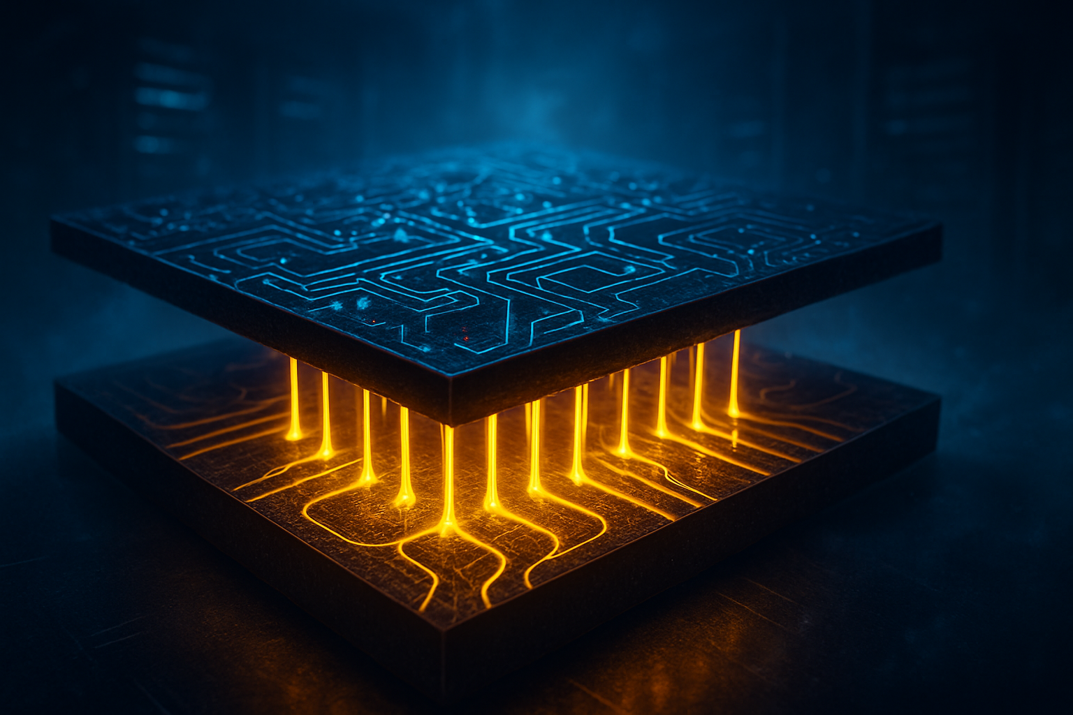
    BSPDN solves this by essentially flipping the house. In this new architecture, the silicon wafer is thinned down to a fraction of its original thickness, and an entirely separate network of power delivery lines is fabricated on the back. Intel Corporation (NASDAQ: INTC) was the first to commercialize this with its PowerVia technology, which utilizes "nano-Through Silicon Vias" (nTSVs) to carry power directly to the transistor layer. This separation allows for much thicker, less resistive power wires on the back and clearer, more efficient signal routing on the front.

    The technical specifications are staggering. Early reports from the 1.8nm (18A) production lines indicate that BSPDN reduces "IR drop"—a phenomenon where voltage decreases as it travels through a circuit—by nearly 30%. This allows transistors to switch faster while consuming less energy. Initial reactions from the research community have highlighted that this shift provides a 6% to 10% frequency boost and up to a 15% reduction in total power loss, a critical requirement for AI chips that are now pushing toward 1,000-watt power envelopes.

    The New Foundry War: Intel, TSMC, and the 2nm Gold Rush

    The successful rollout of BSPDN has reshaped the competitive landscape among the world’s leading foundries. Intel (NASDAQ: INTC) has used its first-mover advantage with PowerVia to reclaim a seat at the table of leading-edge manufacturing. Its 18A node is now in high-volume production, powering the new Panther Lake processors and securing major foundry customers like Microsoft Corporation (NASDAQ: MSFT) and Amazon (NASDAQ: AMZN), both of which are designing custom AI silicon to reduce their reliance on merchant hardware.

    However, Taiwan Semiconductor Manufacturing Company (NYSE: TSM) remains the titan to beat. While TSMC’s initial 2nm (N2) node did not include backside power, its upcoming A16 node—scheduled for mass production later this year—introduces the "Super Power Rail." This implementation is even more advanced than Intel's, connecting power directly to the transistor’s source and drain. This precision has led NVIDIA Corporation (NASDAQ: NVDA) to select TSMC’s A16 for its next-generation "Rubin" AI platform, which aims to deliver a 3x performance-per-watt improvement over the previous Blackwell architecture.

    Meanwhile, Samsung Electronics (OTC: SSNLF) is positioning itself as the "turnkey" alternative. Samsung is skipping the intermediate steps and moving directly to a highly optimized BSPDN on its 2nm (SF2Z) node. By offering a bundled package of 2nm logic, HBM4 memory, and advanced 2.5D packaging, Samsung has managed to peel away high-profile AI startups and even secure contracts from Advanced Micro Devices (NASDAQ: AMD) for specialized AI chiplets.

    AI Scaling and the "Joule-per-Token" Metric

    The broader significance of Backside Power Delivery lies in its impact on the economics of artificial intelligence. In 2026, the focus of the AI industry has shifted from raw FLOPS (Floating Point Operations Per Second) to "Joules-per-Token"—a measure of how much energy it takes to generate a single word of AI output. With the cost of 2nm wafers reportedly reaching $30,000 each, the energy efficiency provided by BSPDN is the only way for hyperscalers to keep the operational costs of LLMs (Large Language Models) sustainable.

    Furthermore, BSPDN is a prerequisite for the continued density of AI accelerators. By freeing up space on the front of the die, designers have been able to increase logic density by 10% to 20%, allowing for more Tensor cores and larger on-chip caches. This is vital for the 2026 crop of "Superchips" that integrate CPUs and GPUs on a single package. Without backside power, these chips would have simply melted under the thermal and electrical stress of modern AI workloads.

    However, this transition has not been without its challenges. One major concern is thermal management. Because the power delivery network is now on the back of the chip, it can trap heat between the silicon and the cooling solution. This has made liquid cooling a mandatory requirement for almost all high-performance AI hardware using these new nodes, leading to a massive infrastructure upgrade cycle in data centers across the globe.

    Looking Ahead: 1nm and the 3D Future

    The shift to BSPDN is not just a one-time upgrade; it is the foundation for the next decade of semiconductor evolution. Looking forward to 2027 and 2028, experts predict the arrival of the 1.4nm and 1nm nodes, where BSPDN will be combined with "Complementary FET" (CFET) architectures. In a CFET design, n-type and p-type transistors are stacked directly on top of each other, a move that would be physically impossible without the backside plumbing provided by BSPDN.

    We are also seeing the early stages of "Function-Side Power Delivery," where specific parts of the chip can be powered independently from the back to allow for ultra-fine-grained power gating. This would allow AI chips to "turn off" 90% of their circuits during idle periods, further driving down the carbon footprint of AI. The primary challenge remaining is yield; as of early 2026, Intel and TSMC are still working to push 2nm/1.8nm yields past the 70% mark, a task complicated by the extreme precision required to align the front and back of the wafer.

    A Fundamental Transformation of Silicon

    The arrival of Backside Power Delivery marks the end of the "Planar Era" and the beginning of a truly three-dimensional approach to computing. By separating the flow of energy from the flow of information, the semiconductor industry has successfully navigated the most dangerous bottleneck in its history.

    The key takeaways for the coming year are clear: Intel has proven its technical relevance with PowerVia, but TSMC’s A16 remains the preferred choice for the highest-end AI hardware. For the tech industry, the 2nm and 1.8nm nodes represent more than just a shrink; they are an architectural rebirth that will define the performance limits of artificial intelligence for years to come. In the coming months, watch for the first third-party benchmarks of Intel’s 18A and the official tape-outs of NVIDIA’s Rubin GPUs—these will be the ultimate tests of whether the "backside revolution" lives up to its immense promise.


    This content is intended for informational purposes only and represents analysis of current AI developments.

    TokenRing AI delivers enterprise-grade solutions for multi-agent AI workflow orchestration, AI-powered development tools, and seamless remote collaboration platforms.
    For more information, visit https://www.tokenring.ai/.
  • The Silent Revolution: How Backside Power Delivery is Shattering the AI Performance Wall

    The Silent Revolution: How Backside Power Delivery is Shattering the AI Performance Wall

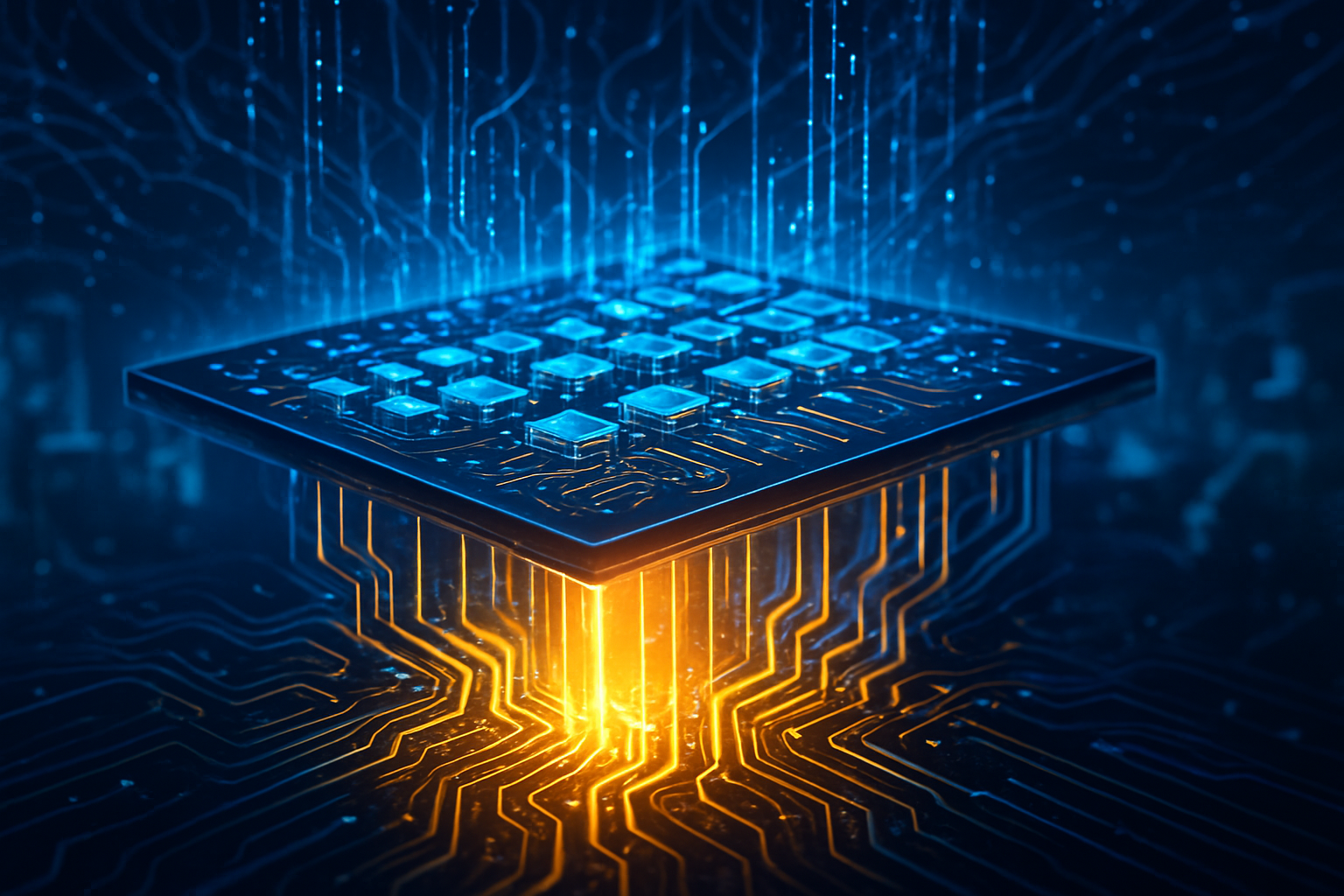
    The semiconductor industry has officially entered the era of Backside Power Delivery (BSPDN), a fundamental architectural shift that marks the most significant change to transistor design in over a decade. As of January 2026, the long-promised "power wall" that threatened to stall AI progress is being dismantled, not by making transistors smaller, but by fundamentally re-engineering how they are powered. This breakthrough, which involves moving the intricate web of power circuitry from the top of the silicon wafer to its underside, is proving to be the secret weapon for the next generation of AI-ready processors.

    The immediate significance of this development cannot be overstated. For years, chip designers have struggled with a "logistical nightmare" on the silicon surface, where power delivery wires and signal routing wires competed for the same limited space. This congestion led to significant electrical efficiency losses and restricted the density of logic gates. With the debut of Intel’s PowerVia and the upcoming arrival of TSMC’s Super Power Rail, the industry is seeing a leap in performance-per-watt that is essential for sustaining the massive computational demands of generative AI and large-scale inference models.

    A Technical Deep Dive: PowerVia vs. Super Power Rail

    At the heart of this revolution are two competing implementations of BSPDN: PowerVia from Intel Corporation (NASDAQ: INTC) and the Super Power Rail (SPR) from Taiwan Semiconductor Manufacturing Company (NYSE: TSM). Intel has successfully taken the first-mover advantage, with its 18A node and Panther Lake processors hitting high-volume manufacturing in late 2025 and appearing in retail systems this month. Intel’s PowerVia utilizes Nano-Through Silicon Vias (nTSVs) to connect the power network on the back of the wafer to the transistors. This implementation has reduced IR drop—the voltage droop that occurs as electricity travels through a chip—from a standard 7% to less than 1%. By clearing the power lines from the frontside, Intel has achieved a staggering 30% increase in transistor density, allowing for more complex AI engines (NPUs) to be packed into smaller footprints.

    TSMC is taking a more aggressive technical path with its Super Power Rail on the A16 node, scheduled for high-volume production in the second half of 2026. Unlike Intel’s nTSV approach, TSMC’s SPR connects the power network directly to the source and drain of the transistors. While significantly harder to manufacture, this "direct contact" method is expected to offer even higher electrical efficiency. TSMC projects that A16 will deliver a 15-20% power reduction at the same clock frequency compared to its 2nm (N2P) process. This approach is specifically engineered to handle the 1,000-watt power envelopes of future data center GPUs, effectively "shattering the performance wall" by allowing chips to sustain peak boost clocks without the electrical instability that plagued previous architectures.

    Strategic Impacts on AI Giants and Startups

    This shift in manufacturing technology is creating a new competitive landscape for AI companies. Intel’s early lead with PowerVia has allowed it to position its Panther Lake chips as the premier platform for "AI PCs," capable of running 70-billion-parameter LLMs locally on thin-and-light laptops. This poses a direct challenge to competitors who are still reliant on traditional frontside power delivery. For startups and independent AI labs, the increased density means that custom silicon—previously too expensive or complex to design—is becoming more viable, as BSPDN simplifies the physical design rules for high-performance logic.

    Meanwhile, the anticipation for TSMC’s A16 node has already sparked a gold rush among the industry’s heavyweights. Nvidia (NASDAQ: NVDA) is reportedly the anchor customer for A16, intending to use the Super Power Rail to power its 2027 "Feynman" GPU architecture. The ability of A16 to deliver stable, high-amperage power directly to the transistor source is critical for Nvidia’s roadmap, which requires increasingly massive parallel throughput. For cloud giants like Amazon (NASDAQ: AMZN) and Google (NASDAQ: GOOGL), who are developing their own internal AI accelerators (Trainium and TPU), the choice between Intel’s available 18A and TSMC’s upcoming A16 will define their infrastructure efficiency and operational costs for the next three years.

    The Broader Significance: Beyond Moore's Law

    Backside Power Delivery represents more than just a clever engineering trick; it is a paradigm shift that extends the viability of Moore’s Law. As transistors shrunk toward the 2nm and 1.6nm scales, the "wiring bottleneck" became the primary limiting factor in chip performance. By separating the power and data highways into two distinct layers, the industry has effectively doubled the available "real estate" on the chip. This fits into the broader trend of "system-technology co-optimization" (STCO), where the physical structure of the chip is redesigned to meet the specific requirements of AI workloads, which are uniquely sensitive to latency and power fluctuations.

    However, this transition is not without concerns. Moving power to the backside requires complex wafer-thinning and bonding processes that increase the risk of manufacturing defects. Thermal management also becomes more complex; while moving the power grid closer to the cooling solution can help, the extreme power density of these chips creates localized "hot spots" that require advanced liquid cooling or even diamond-based heat spreaders. Compared to previous milestones like the introduction of FinFET transistors, the move to BSPDN is arguably more disruptive because it changes the entire vertical stack of the semiconductor manufacturing process.

    The Horizon: What Comes After 18A and A16?

    Looking ahead, the successful deployment of BSPDN paves the way for the "1nm era" and beyond. In the near term, we expect to see "Backside Signal Routing," where not just power, but also some global clock and data signals are moved to the underside of the wafer to further reduce interference. Experts predict that by 2028, we will see the first true "3D-stacked" logic, where multiple layers of transistors are sandwiched between multiple layers of backside and frontside routing, leading to a ten-fold increase in AI compute density.

    The primary challenge moving forward will be the cost of these advanced nodes. The equipment required for backside processing—specifically advanced wafer bonders and thinning tools—is incredibly expensive, which may lead to a widening gap between the "compute-rich" companies that can afford 1.6nm silicon and those stuck on older, frontside-powered nodes. As AI models continue to grow in size, the ability to manufacture these high-density, high-efficiency chips will become a matter of national economic security, further accelerating the "chip wars" between global superpowers.

    Closing Thoughts on the BSPDN Era

    The transition to Backside Power Delivery marks a historic moment in computing. Intel’s PowerVia has proven that the technology is ready for the mass market today, while TSMC’s Super Power Rail promises to push the boundaries of what is electrically possible by the end of the year. The key takeaway is that the "power wall" is no longer a fixed barrier; it is a challenge that has been solved through brilliant architectural innovation.

    As we move through 2026, the industry will be watching the yields of TSMC’s A16 node and the adoption rates of Intel’s 18A-based Clearwater Forest Xeons. For the AI industry, these technical milestones translate directly into faster training times, more efficient inference, and the ability to run more sophisticated models on everyday devices. The silent revolution on the underside of the silicon wafer is, quite literally, powering the future of intelligence.


    This content is intended for informational purposes only and represents analysis of current AI developments.

    TokenRing AI delivers enterprise-grade solutions for multi-agent AI workflow orchestration, AI-powered development tools, and seamless remote collaboration platforms.
    For more information, visit https://www.tokenring.ai/.
  • The Great Flip: How Backside Power Delivery is Redefining the Race to Sub-2nm AI Chips

    The Great Flip: How Backside Power Delivery is Redefining the Race to Sub-2nm AI Chips

    As of January 13, 2026, the semiconductor industry has officially entered the "Angstrom Era," a transition marked by the most significant architectural overhaul in over a decade. For fifty years, chipmakers have followed a "front-side" logic: transistors are built on a silicon wafer, and then layers of intricate copper wiring for both data signals and power are stacked on top. However, as AI accelerators and processors shrink toward the sub-2nm threshold, this traditional "spaghetti" of overlapping wires has become a physical bottleneck, leading to massive voltage drops and heat-related performance throttling.

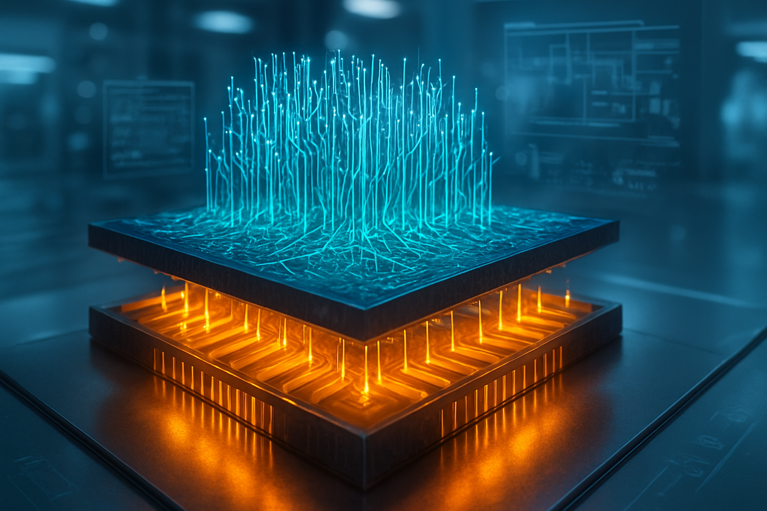
    The solution, now being deployed in high-volume manufacturing by industry leaders, is Backside Power Delivery Network (BSPDN). By flipping the wafer and moving the power delivery grid to the bottom—decoupling it entirely from the signal wiring—foundries are finally breaking through the "Power Wall" that has long threatened to stall the AI revolution. This architectural shift is not merely a refinement; it is a fundamental restructuring of the silicon floorplan that enables the next generation of 1,000W+ AI GPUs and hyper-efficient mobile processors.

    The Technical Duel: Intel’s PowerVia vs. TSMC’s Super Power Rail

    At the heart of this transition is a fierce technical rivalry between Intel (NASDAQ: INTC) and Taiwan Semiconductor Manufacturing Company (NYSE: TSM). Intel has successfully claimed a "first-mover" advantage with its PowerVia technology, integrated into the Intel 18A (1.8nm) node. PowerVia utilizes "Nano-TSVs" (Through-Silicon Vias) that tunnel through the silicon from the backside to connect to the metal layers just above the transistors. This implementation has allowed Intel to achieve a 30% reduction in platform voltage droop and a 6% boost in clock frequency at identical power levels. By January 2026, Intel’s 18A is in high-volume manufacturing, powering the "Panther Lake" and "Clearwater Forest" chips, effectively proving that BSPDN is viable for mass-market consumer and server silicon.

    TSMC, meanwhile, has taken a more complex and potentially more rewarding path with its A16 (1.6nm) node, featuring the Super Power Rail. Unlike Intel’s Nano-TSVs, TSMC’s architecture uses a "Direct Backside Contact" method, where power lines connect directly to the source and drain terminals of the transistors. While this requires extreme manufacturing precision and alignment, it offers superior performance metrics: an 8–10% speed increase and a 15–20% power reduction compared to their previous N2P node. TSMC is currently in the final stages of risk production for A16, with full-scale manufacturing expected in the second half of 2026, targeting the absolute limits of power integrity for high-performance computing (HPC).

    Initial reactions from the AI research community have been overwhelmingly positive, with experts noting that BSPDN effectively "reclaims" 20% to 30% of the front-side metal layers. This allows chip designers to use the newly freed space for more complex signal routing, which is critical for the high-bandwidth memory (HBM) and interconnects required for large language model (LLM) training. The industry consensus is that while Intel won the race to market, TSMC’s direct-contact approach may set the gold standard for the most demanding AI accelerators of 2027 and beyond.

    Shifting the Competitive Balance: Winners and Losers in the Foundry War

    The arrival of BSPDN has drastically altered the strategic positioning of the world’s largest tech companies. Intel’s successful execution of PowerVia on 18A has restored its credibility as a leading-edge foundry, securing high-profile "AI-first" customers like Microsoft (NASDAQ: MSFT) and Amazon (NASDAQ: AMZN). These companies are utilizing Intel’s 18A to develop custom AI accelerators, seeking to reduce their reliance on off-the-shelf hardware by leveraging the density and power efficiency gains that only BSPDN can provide. For Intel, this is a "make-or-break" moment to regain the process leadership it lost to TSMC nearly a decade ago.

    TSMC, however, remains the primary partner for the AI heavyweights. NVIDIA (NASDAQ: NVDA) has reportedly signed on as the anchor customer for TSMC’s A16 node for its 2027 "Feynman" GPU architecture. As AI chips push toward 2,000W power envelopes, NVIDIA’s strategic advantage lies in TSMC’s Super Power Rail, which minimizes the electrical resistance that would otherwise cause catastrophic heat generation. Similarly, AMD (NASDAQ: AMD) is expected to adopt a modular approach, using TSMC’s N2 for general logic while reserving the A16 node for high-performance compute chiplets in its upcoming MI400 series.

    Samsung (KRX: 005930), the third major player, is currently playing catch-up. While Samsung’s SF2 (2nm) node is in mass production and powering the latest Exynos mobile chips, it uses only "preliminary" power rail optimizations. Samsung’s full BSPDN implementation, SF2Z, is not scheduled until 2027. To remain competitive, Samsung has aggressively slashed its 2nm wafer prices to attract cost-conscious AI startups and automotive giants like Tesla (NASDAQ: TSLA), positioning itself as the high-volume, lower-cost alternative to TSMC’s premium A16 pricing.

    The Wider Significance: Breaking the Power Wall and Enabling AI Scaling

    The broader significance of Backside Power Delivery cannot be overstated; it is the "Great Flip" that saves Moore’s Law from thermal death. As transistors have shrunk, the wires connecting them have become so thin that their electrical resistance has skyrocketed. This has led to the "Power Wall," where a chip’s performance is limited not by how many transistors it has, but by how much power can be fed to them without the chip melting. BSPDN solves this by providing a "fat," low-resistance highway for electricity on the back of the chip, reducing the IR drop (voltage drop) by up to 7x.

    This development fits into a broader trend of "3D Silicon" and advanced packaging. By thinning the silicon wafer to just a few micrometers to allow for backside access, the heat-generating transistors are placed physically closer to the cooling solutions—such as liquid cold plates—on the back of the chip. This improved thermal proximity is essential for the 2026-2027 generation of data centers, where power density is the primary constraint on AI training capacity.

    Compared to previous milestones like the introduction of FinFET transistors in 2011, the move to BSPDN is considered more disruptive because it requires a complete overhaul of the Electronic Design Automation (EDA) tools used by engineers. Design teams at companies like Synopsys (NASDAQ: SNPS) and Cadence (NASDAQ: CDNS) have had to rewrite their software to handle "backside-aware" placement and routing, a change that will define chip design for the next twenty years.

    Future Horizons: High-NA EUV and the Path to 1nm

    Looking ahead, the synergy between BSPDN and High-Numerical Aperture (High-NA) EUV lithography will define the path to the 1nm (10 Angstrom) frontier. Intel is currently the leader in this integration, already sampling its 14A node which combines High-NA EUV with an evolved version of PowerVia. While High-NA EUV allows for the printing of smaller features, it also makes those features more electrically fragile; BSPDN acts as the necessary electrical support system that makes these microscopic features functional.

    In the near term, expect to see "Hybrid Backside" approaches, where not just power, but also certain clock signals and global wires are moved to the back of the wafer. This would further reduce noise and interference, potentially allowing for the first 6GHz+ mobile processors. However, challenges remain, particularly regarding the structural integrity of ultra-thin wafers and the complexity of testing chips from both sides. Experts predict that by 2028, backside delivery will be standard for all high-end silicon, from the chips in your smartphone to the massive clusters powering the next generation of General Artificial Intelligence.

    Conclusion: A New Foundation for the Intelligence Age

    The transition to Backside Power Delivery marks the end of the "Planar Power" era and the beginning of a truly three-dimensional approach to semiconductor architecture. By decoupling power from signal, Intel and TSMC have provided the industry with a new lease on life, enabling the sub-2nm scaling that is vital for the continued growth of AI. Intel’s early success with PowerVia has tightened the race for process leadership, while TSMC’s ambitious Super Power Rail ensures that the ceiling for AI performance continues to rise.

    As we move through 2026, the key metrics to watch will be the manufacturing yields of TSMC’s A16 node and the adoption rate of Intel’s 18A by external foundry customers. The "Great Flip" is more than a technical curiosity; it is the hidden infrastructure that will determine which companies lead the next decade of AI innovation. The foundation of the intelligence age is no longer just on top of the silicon—it is now on the back.


    This content is intended for informational purposes only and represents analysis of current AI developments.

    TokenRing AI delivers enterprise-grade solutions for multi-agent AI workflow orchestration, AI-powered development tools, and seamless remote collaboration platforms.
    For more information, visit https://www.tokenring.ai/.
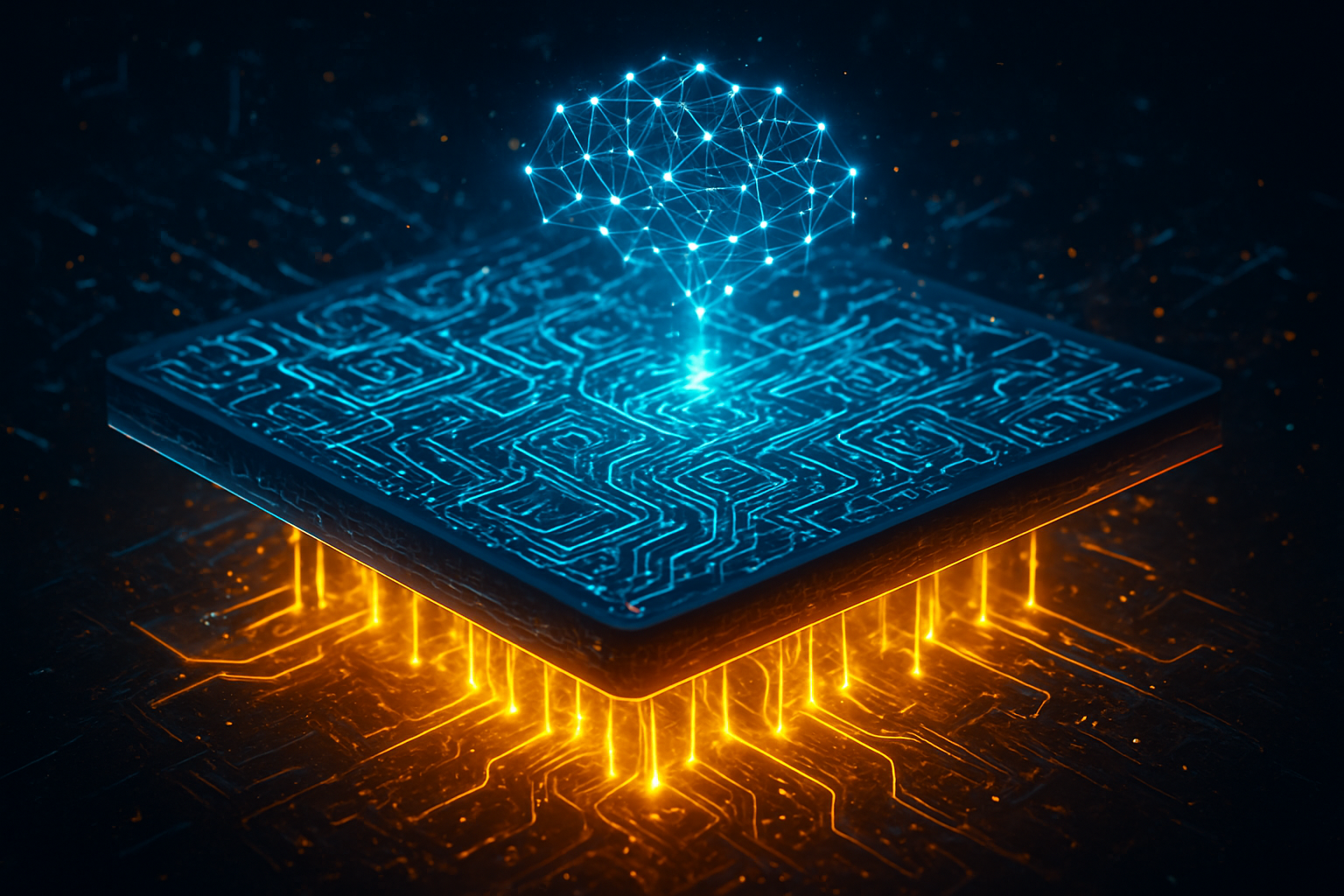
  • The Power Flip: How Backside Delivery is Rescuing the 1,000W AI Era

    The Power Flip: How Backside Delivery is Rescuing the 1,000W AI Era

    The semiconductor industry has officially entered the "Angstrom Era," marked by the most radical architectural shift in chip manufacturing in over three decades. As of January 5, 2026, the traditional method of routing power through the front of a silicon wafer—a practice that has persisted since the dawn of the integrated circuit—is being abandoned in favor of Backside Power Delivery Networks (BSPDN). This transition is not merely an incremental improvement; it is a fundamental necessity driven by the insatiable energy demands of generative AI and the physical limitations of atomic-scale transistors.

    The immediate significance of this shift was underscored today at CES 2026, where Intel Corporation (Nasdaq:INTC) announced the broad market availability of its "Panther Lake" processors, the first consumer-grade chips to utilize high-volume backside power. By decoupling the power delivery from the signal routing, chipmakers are finally solving the "wiring bottleneck" that has plagued the industry. This development ensures that the next generation of AI accelerators, which are now pushing toward 1,000W to 1,500W per module, can receive stable electricity without the catastrophic voltage losses that would have rendered them inefficient or unworkable on older architectures.

    The Technical Divorce: PowerVia vs. Super Power Rail

    At the heart of this revolution are two competing technical philosophies: Intel’s PowerVia and Taiwan Semiconductor Manufacturing Company’s (NYSE:TSM) Super Power Rail. Historically, both power and data signals were routed through a complex "jungle" of metal layers on top of the transistors. As transistors shrunk to the 2nm and 1.8nm levels, these wires became so thin and crowded that resistance skyrocketed, leading to significant "IR drop"—a phenomenon where voltage decreases as it travels through the chip. BSPDN solves this by moving the power delivery to the reverse side of the wafer, effectively giving the chip two "fronts": one for data and one for energy.

    Intel’s PowerVia, debuting in the 18A (1.8nm) process node, utilizes a "nano-TSV" (Through Silicon Via) approach. In this implementation, Intel builds the transistors first, then flips the wafer to create small vertical connections that bridge the backside power layers to the metal layers on the front. This method is considered more manufacturable and has allowed Intel to claim a first-to-market advantage. Early data from Panther Lake production indicates a 30% improvement in voltage droop and a 6% frequency boost at identical power levels compared to traditional front-side delivery. Furthermore, by clearing the "congestion" on the front side, Intel has achieved a staggering 90% standard cell utilization, drastically increasing logic density.

    TSMC is taking a more aggressive, albeit delayed, approach with its A16 (1.6nm) node and its "Super Power Rail" technology. Unlike Intel’s nano-TSVs, TSMC’s implementation connects the backside power network directly to the source and drain of the transistors. This direct-contact method is significantly more complex to manufacture, requiring advanced material science to prevent contamination during the bonding process. However, the theoretical payoff is higher: TSMC targets an 8–10% speed improvement and up to a 20% power reduction. While Intel is shipping products today, TSMC is positioning its Super Power Rail as the "refined" version of BSPDN, slated for mass production in the second half of 2026 to power the next generation of high-end AI and mobile silicon.

    Strategic Dominance and the AI Arms Race

    The shift to backside power has created a new competitive landscape for tech giants and specialized AI labs. Intel’s early lead with 18A and PowerVia is a strategic masterstroke for its Foundry business. By proving the viability of BSPDN in high-volume consumer chips like Panther Lake, Intel is signaling to major fabless customers that it has solved the most difficult scaling challenge of the decade. This puts immense pressure on Samsung Electronics (KRX:005930), which is also racing to implement its own BSPDN version to remain competitive in the logic foundry market.

    For AI powerhouses like NVIDIA (Nasdaq:NVDA), the arrival of BSPDN is a lifeline. NVIDIA’s current "Blackwell" architecture and the upcoming "Rubin" platform (scheduled for late 2026) are pushing the limits of data center power infrastructure. With GPUs now drawing well over 1,000W, traditional power delivery would result in massive heat generation and energy waste. By adopting TSMC’s A16 process and Super Power Rail, NVIDIA can ensure that its future Rubin GPUs maintain high clock speeds and reliability even under the extreme workloads required for training trillion-parameter models.

    The primary beneficiaries of this development are the "Magnificent Seven" and other hyperscalers who operate massive data centers. Companies like Apple (Nasdaq:AAPL) and Alphabet (Nasdaq:GOOGL) are already reportedly in the queue for TSMC’s A16 capacity. The ability to pack more compute into the same thermal envelope allows these companies to maximize their return on investment for AI infrastructure. Conversely, startups that cannot secure early access to these advanced nodes may find themselves at a performance-per-watt disadvantage, potentially widening the gap between the industry leaders and the rest of the field.

    Solving the 1,000W Crisis in the AI Landscape

    The broader significance of BSPDN lies in its role as a "force multiplier" for AI scaling laws. For years, experts have worried that we would hit a "power wall" where the energy required to drive a chip would exceed its ability to dissipate heat. BSPDN effectively moves that wall. By thinning the silicon wafer to allow for backside connections, chipmakers also improve the thermal path from the transistors to the cooling solution. This is critical for the 1,000W+ power demands of modern AI accelerators, which would otherwise face severe thermal throttling.

    This architectural change mirrors previous industry milestones, such as the transition from planar transistors to FinFETs in the early 2010s. Just as FinFETs allowed the industry to continue scaling despite leakage current issues, BSPDN allows scaling to continue despite resistance issues. However, the transition is not without concerns. The manufacturing process for BSPDN is incredibly delicate; it involves bonding two wafers together with nanometer precision and then grinding one down to a thickness of just a few hundred nanometers. Any misalignment can result in total wafer loss, making yield management the primary challenge for 2026.

    Moreover, the environmental impact of this technology is a double-edged sword. While BSPDN makes chips more efficient on a per-calculation basis, the sheer performance gains it enables are likely to encourage even larger, more power-hungry AI clusters. As the industry moves toward 600kW racks for data centers, the efficiency gains of backside power will be essential just to keep the lights on, though they may not necessarily reduce the total global energy footprint of AI.

    The Horizon: Beyond 1.6 Nanometers

    Looking ahead, the successful deployment of PowerVia and Super Power Rail sets the stage for the sub-1nm era. Industry experts predict that the next logical step after BSPDN will be the integration of "optical interconnects" directly onto the backside of the die. Once the power delivery has been moved to the rear, the front side is theoretically "open" for even more dense signal routing, including light-based data transmission that could eliminate traditional copper wiring altogether for long-range on-chip communication.

    In the near term, the focus will shift to how these technologies handle the "Rubin" generation of GPUs and the "Panther Lake" successor, "Nova Lake." The challenge remains the cost: the complexity of backside power adds significant steps to the lithography process, which will likely keep the price of advanced AI silicon high. Analysts expect that by 2027, BSPDN will be the standard for all high-performance computing (HPC) chips, while budget-oriented mobile chips may stick to traditional front-side delivery for another generation to save on manufacturing costs.

    A New Foundation for Silicon

    The arrival of Backside Power Delivery marks a pivotal moment in the history of computing. It represents a "flipping of the script" in how we design and build the brains of our digital world. By physically separating the two most critical components of a chip—its energy and its information—engineers have unlocked a new path for Moore’s Law to continue into the Angstrom Era.

    The key takeaways from this transition are clear: Intel has successfully reclaimed a technical lead by being the first to market with PowerVia, while TSMC is betting on a more complex, higher-performance implementation to maintain its dominance in the AI accelerator market. As we move through 2026, the industry will be watching yield rates and the performance of NVIDIA’s next-generation chips to see which approach yields the best results. For now, the "Power Flip" has successfully averted a scaling crisis, ensuring that the next wave of AI breakthroughs will have the energy they need to come to life.


    This content is intended for informational purposes only and represents analysis of current AI developments.

    TokenRing AI delivers enterprise-grade solutions for multi-agent AI workflow orchestration, AI-powered development tools, and seamless remote collaboration platforms.
    For more information, visit https://www.tokenring.ai/.

  • Samsung’s AI Foundry Ambitions: Challenging the Semiconductor Giants

    Samsung’s AI Foundry Ambitions: Challenging the Semiconductor Giants

    In a bold strategic maneuver, Samsung (KRX: 005930) is aggressively expanding its foundry business, setting its sights firmly on capturing a larger, more influential share of the burgeoning Artificial Intelligence (AI) chip market. This ambitious push, underpinned by multi-billion dollar investments and pioneering technological advancements, aims to position the South Korean conglomerate as a crucial "one-stop shop" solution provider for the entire AI chip development and manufacturing lifecycle. The immediate significance of this strategy lies in its potential to reshape the global semiconductor landscape, intensifying competition with established leaders like TSMC (NYSE: TSM) and Intel (NASDAQ: INTC), and accelerating the pace of AI innovation worldwide.

    Samsung's integrated approach leverages its unparalleled expertise across memory chips, foundry services, and advanced packaging technologies. By streamlining the entire production process, the company anticipates reducing manufacturing times by approximately 20%, a critical advantage in the fast-evolving AI sector where time-to-market is paramount. This holistic offering is particularly attractive to fabless AI chip designers seeking high-performance, low-power, and high-bandwidth solutions, offering them a more cohesive and efficient path from design to deployment.

    Detailed Technical Coverage

    At the heart of Samsung's AI foundry ambitions are its groundbreaking technological advancements, most notably the Gate-All-Around (GAA) transistor architecture, aggressive pursuit of sub-2nm process nodes, and the innovative Backside Power Delivery Network (BSPDN). These technologies represent a significant leap forward from previous semiconductor manufacturing paradigms, designed to meet the extreme computational and power efficiency demands of modern AI workloads.

    Samsung was an early adopter of GAA technology, initiating mass production of its 3-nanometer (nm) process with GAA (called MBCFET™) in 2022. Unlike the traditional FinFET design, where the gate controls the channel on three sides, GAAFETs completely encircle the channel on all four sides. This superior electrostatic control dramatically reduces leakage current and improves power efficiency, enabling chips to operate faster with less energy – a vital attribute for AI accelerators. Samsung's MBCFET design further enhances this by using nanosheets with adjustable widths, offering greater flexibility for optimizing power and performance compared to the fixed fin counts of FinFETs. Compared to its previous 5nm process, Samsung's 3nm GAA technology consumes 45% less power and occupies 16% less area, with the second-generation GAA further boosting performance by 30% and power efficiency by 50%.

    The company's roadmap for process node scaling is equally aggressive. Samsung plans to begin mass production of its 2nm process (SF2) for mobile applications in 2025, expanding to high-performance computing (HPC) chips in 2026 and automotive chips in 2027. An advanced variant, SF2Z, slated for mass production in 2027, will incorporate Backside Power Delivery Network (BSPDN) technology. BSPDN is a revolutionary approach that relocates power lines to the backside of the silicon wafer, separating them from the signal network on the front. This alleviates congestion, significantly reduces voltage drop (IR drop), and improves power delivery efficiency, leading to enhanced performance and area optimization. Samsung claims BSPDN can reduce the size of its 2nm chip by 17%, improve performance by 8%, and power efficiency by 15% compared to traditional front-end power delivery. Furthermore, Samsung has confirmed plans for mass production of its more advanced 1.4nm (SF1.4) chips by 2027.

    Initial reactions from the AI research community and industry experts have been largely positive, recognizing these technical breakthroughs as foundational enablers for the next wave of AI innovation. Experts emphasize that GAA and BSPDN are crucial for overcoming the physical limits of FinFETs and addressing critical bottlenecks like power density and thermal dissipation in increasingly complex AI models. Samsung itself highlights that its GAA-based advanced node technology will be "instrumental in supporting the needs of our customers using AI applications," and its integrated "one-stop AI solutions" are designed to speed up AI chip production by 20%. While historical challenges with yield rates for advanced nodes have been noted, recent reports of securing multi-billion dollar agreements for AI-focused chips on its 2nm platform suggest growing confidence in Samsung's capabilities.

    Impact on AI Companies, Tech Giants, and Startups

    Samsung's advanced foundry strategy, encompassing GAA, aggressive node scaling, and BSPDN, is poised to profoundly affect AI companies, tech giants, and startups by offering a compelling alternative in the high-stakes world of AI chip manufacturing. Its "one-stop shop" approach, integrating memory, foundry, and advanced packaging, is designed to streamline the entire chip production process, potentially cutting turnaround times significantly.

    Fabless AI chip designers, including major players like NVIDIA (NASDAQ: NVDA) and AMD (NASDAQ: AMD), which have historically relied heavily on TSMC, stand to benefit immensely from Samsung's increasingly competitive offerings. A crucial second source for advanced manufacturing can enhance supply chain resilience, foster innovation through competition, and potentially lead to more favorable pricing. A prime example of this is the monumental $16.5 billion multi-year deal with Tesla (NASDAQ: TSLA), where Samsung will produce Tesla's next-generation AI6 inference chips on its 2nm process at a dedicated fabrication plant in Taylor, Texas. This signifies a strong vote of confidence in Samsung's capabilities for AI in autonomous vehicles and robotics. Qualcomm (NASDAQ: QCOM) is also reportedly considering Samsung's 2nm foundry process. Companies requiring tightly integrated memory and logic for their AI solutions will find Samsung's vertical integration a compelling advantage.

    The competitive landscape of the foundry market is heating up considerably. TSMC remains the undisputed leader, especially in advanced nodes and packaging solutions like CoWoS, which are critical for AI accelerators. TSMC plans to introduce 2nm (N2) with GAA transistors in late 2025 and 1.6nm (A16) with BSPDN by late 2026. Intel Foundry Services (IFS) is also aggressively pursuing a "five nodes in four years" plan, with its 18A process incorporating GAA (RibbonFET) and BSPDN (PowerVia), aiming to compete with TSMC's N2 and Samsung's SF2. Samsung's advancements intensify this three-way race, potentially driving down costs, accelerating innovation, and offering more diverse options for AI chip design and manufacturing. This competition doesn't necessarily disrupt existing products as much as it enables and accelerates their capabilities, pushing the boundaries of what AI chips can achieve.

    For startups developing specialized AI-oriented processors, Samsung's Advanced Foundry Ecosystem (SAFE) program and partnerships with design solution providers aim to offer a more accessible development path. This enables smaller entities to bring innovative AI hardware to market more efficiently. Samsung is also strategically backing external AI chip startups, such as its $250 million investment in South Korean startup Rebellions (private), aiming to secure future major foundry clients. Samsung is positioning itself as a critical enabler of the AI revolution, aiming for its AI-related customer base to grow fivefold and revenue to increase ninefold by 2028. Its unique vertical integration, early GAA adoption, aggressive node roadmap, and strategic partnerships provide significant advantages in this high-stakes market.

    Wider Significance

    Samsung's intensified foray into the AI foundry business holds profound wider significance for the entire AI industry, fitting squarely into the broader trends of escalating computational demands and the pursuit of specialized hardware. The current AI landscape, dominated by the insatiable appetite for powerful and efficient chips for generative AI and large language models (LLMs), finds a crucial response in Samsung's integrated "one-stop shop" approach. This streamlining of the entire chip production process, from design to advanced packaging, is projected to cut turnaround times by approximately 20%, significantly accelerating the development and deployment of AI models.

    The impacts on the future of AI development are substantial. By providing high-performance, low-power semiconductors through advanced process nodes like 2nm and 1.4nm, coupled with GAA and BSPDN, Samsung is directly contributing to the acceleration of AI innovation. This means faster iteration cycles for AI researchers and developers, leading to quicker breakthroughs and the enablement of more sophisticated AI applications across diverse sectors such as autonomous driving, real-time video analysis, healthcare, and finance. The $16.5 billion deal with Tesla (NASDAQ: TSLA) to produce next-generation AI6 chips for autonomous driving underscores this transformative potential. Furthermore, Samsung's push, particularly with its integrated solutions, aims to attract a broader customer base, potentially leading to more diverse and customized AI hardware solutions, fostering competition and reducing reliance on a single vendor.

    However, this intensified competition and the pursuit of advanced manufacturing also bring potential concerns. The semiconductor manufacturing industry remains highly concentrated, with TSMC (NYSE: TSM) and Samsung (KRX: 005930) being the primary players for cutting-edge nodes. While Samsung's efforts can somewhat alleviate the extreme reliance on TSMC, the overall concentration of advanced chip manufacturing in a few regions (e.g., Taiwan and South Korea) remains a significant geopolitical risk. A disruption in these regions due to geopolitical conflict or natural disaster could severely impact the global AI infrastructure. The "chip war" between the US and China further complicates matters, with export controls and increased investment in domestic production by various nations entangling Samsung's operations. Samsung has also faced challenges with production delays and qualifying advanced memory chips for key partners like NVIDIA (NASDAQ: NVDA), which highlights the difficulties in scaling such cutting-edge technologies.

    Comparing this moment to previous AI milestones in hardware manufacturing reveals a recurring pattern. Just as the advent of transistors and integrated circuits in the mid-20th century revolutionized computing, and the emergence of Graphics Processing Units (GPUs) in the late 1990s (especially NVIDIA's CUDA in 2006) enabled the deep learning revolution, Samsung's current foundry push represents the latest iteration of such hardware breakthroughs. By continually pushing the boundaries of semiconductor technology with advanced nodes, GAA, advanced packaging, and integrated solutions, Samsung aims to provide the foundational hardware that will enable the next wave of AI innovation, much like its predecessors did in their respective eras.

    Future Developments

    Samsung's AI foundry ambitions are set to unfold with a clear roadmap of near-term and long-term developments, promising significant advancements in AI chip manufacturing. In the near-term (1-3 years), Samsung will focus heavily on its "one-stop shop" approach, integrating memory (especially High-Bandwidth Memory – HBM), foundry, and advanced packaging to reduce AI chip production schedules by approximately 20%. The company plans to mass-produce its second-generation 3nm process (SF3) in the latter half of 2024 and its SF4U (4nm variant) in 2025. Crucially, mass production of the 2nm GAA-based SF2 node is scheduled for 2025, with the enhanced SF2Z, featuring Backside Power Delivery Network (BSPDN), slated for 2027. Strategic partnerships, such as the deal with OpenAI (private) for advanced memory chips and the $16.5 billion contract with Tesla (NASDAQ: TSLA) for AI6 chips, will be pivotal in establishing Samsung's presence.

    Looking further ahead (3-10 years), Samsung plans to mass-produce 1.4nm (SF1.4) chips by 2027, with explorations into even more advanced nodes through material and structural innovations. The long-term vision includes a holistic approach to chip architecture, integrating advanced packaging, memory, and specialized accelerators, with AI itself playing an increasing role in optimizing chip design and improving yield management. By 2027, Samsung also aims to introduce an all-in-one, co-packaged optics (CPO) integrated AI solution for high-speed, low-power data processing. These advancements are designed to power a wide array of applications, from large-scale AI model training in data centers and high-performance computing (HPC) to real-time AI inference in edge devices like smartphones, autonomous vehicles, robotics, and smart home appliances.

    However, Samsung faces several significant challenges. A primary concern is improving yield rates for its advanced nodes, particularly for its 2nm technology, targeting 60% by late 2025 from an estimated 30% in 2024. Intense competition from TSMC (NYSE: TSM), which currently dominates the foundry market, and Intel Foundry Services (NASDAQ: INTC), which is aggressively re-entering the space, also poses a formidable hurdle. Geopolitical factors, including U.S. sanctions and the global push for diversified supply chains, add complexity but also present opportunities for Samsung. Experts predict that global chip industry revenue from AI processors could reach $778 billion by 2028, with AI chip demand outpacing traditional semiconductors. While TSMC is projected to retain a significant market share, analysts suggest Samsung could capture 10-15% of the foundry market by 2030 if it successfully addresses its yield issues and accelerates GAA adoption. The "AI infrastructure arms race," driven by initiatives like OpenAI's "Stargate" project, will lead to deeper integration between AI model developers and hardware manufacturers, making access to cutting-edge silicon paramount for future AI progress.

    Comprehensive Wrap-up

    Samsung's (KRX: 005930) "AI Foundry Ambitions" represent a bold and strategically integrated approach to capitalize on the explosive demand for AI chips. The company's unique "one-stop shop" model, combining its strengths in memory, foundry services, and advanced packaging, is a key differentiator, promising reduced production times and optimized solutions for the most demanding AI applications. This strategy is built on a foundation of pioneering technological advancements, including the widespread adoption of Gate-All-Around (GAA) transistor architecture, aggressive scaling to 2nm and 1.4nm process nodes, and the integration of Backside Power Delivery Network (BSPDN) technology. These innovations are critical for delivering the high-performance, low-power semiconductors essential for the next generation of AI.

    The significance of this development in AI history cannot be overstated. By intensifying competition in the advanced foundry market, Samsung is not only challenging the long-standing dominance of TSMC (NYSE: TSM) but also fostering an environment of accelerated innovation across the entire AI hardware ecosystem. This increased competition can lead to faster technological advancements, potentially lower costs, and more diverse manufacturing options for AI developers and companies worldwide. The integrated solutions offered by Samsung, coupled with strategic partnerships like those with Tesla (NASDAQ: TSLA) and OpenAI (private), are directly contributing to building the foundational hardware infrastructure required for the expansion of global AI capabilities, driving the "AI supercycle" forward.

    Looking ahead, the long-term impact of Samsung's strategy could be transformative, potentially reshaping the foundry landscape into a more balanced competitive environment. Success in improving yield rates for its advanced nodes and securing more major AI contracts will be crucial for Samsung to significantly alter market dynamics. The widespread adoption of more efficient AI chips will likely accelerate AI deployment across various industries, from autonomous vehicles to enterprise AI solutions. What to watch for in the coming weeks and months includes Samsung's progress on its 2nm yield rates, announcements of new major fabless customers, the successful ramp-up of its Taylor, Texas plant, and continued advancements in HBM (High-Bandwidth Memory) and advanced packaging technologies. The competitive responses from TSMC and Intel (NASDAQ: INTC) will also be key indicators of how this high-stakes race for AI hardware leadership will unfold, ultimately dictating the pace and direction of AI innovation for the foreseeable future.

    This content is intended for informational purposes only and represents analysis of current AI developments.

    TokenRing AI delivers enterprise-grade solutions for multi-agent AI workflow orchestration, AI-powered development tools, and seamless remote collaboration platforms.
    For more information, visit https://www.tokenring.ai/.