Tag: CES 2026

  • The Dawn of the Rubin Era: NVIDIA’s Six-Chip Architecture Promises to Slash AI Costs by 10x

    The Dawn of the Rubin Era: NVIDIA’s Six-Chip Architecture Promises to Slash AI Costs by 10x

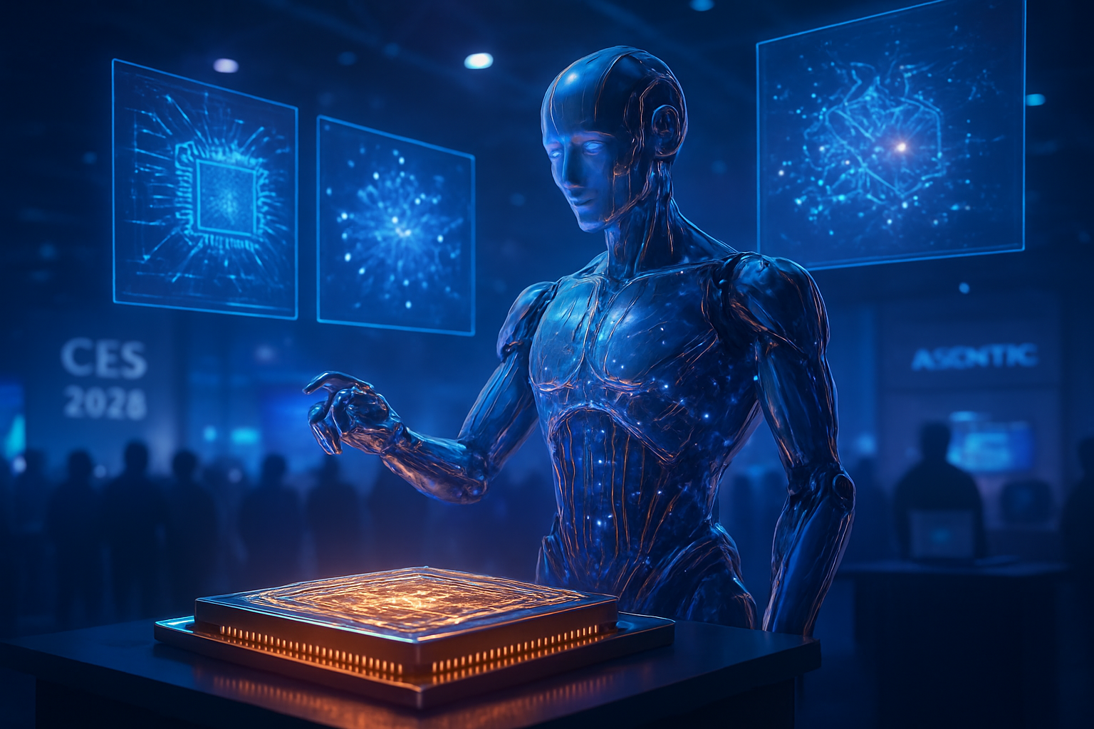
    At the opening keynote of CES 2026 in Las Vegas, NVIDIA (NASDAQ: NVDA) CEO Jensen Huang stood before a packed audience to unveil the Rubin architecture, a technological leap that signals the end of the "Blackwell" era and the beginning of a new epoch in accelerated computing. Named after the pioneering astronomer Vera Rubin, the new platform is not merely a faster graphics processor; it is a meticulously "extreme-codesigned" ecosystem intended to serve as the foundational bedrock for the next generation of agentic AI and trillion-parameter reasoning models.

    The announcement sent shockwaves through the industry, primarily due to NVIDIA’s bold claim that the Rubin platform will reduce AI inference token costs by a staggering 10x. By integrating compute, networking, and memory into a unified "AI factory" design, NVIDIA aims to make persistent, always-on AI agents economically viable for the first time, effectively democratizing high-level intelligence at a scale previously thought impossible.

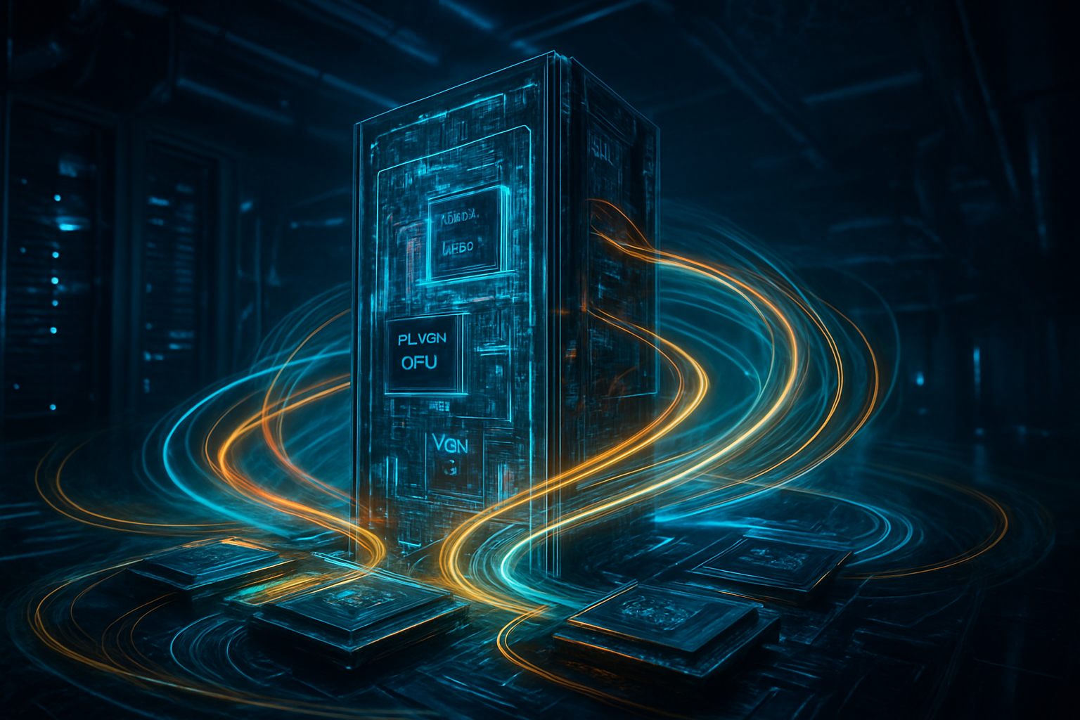
    The Six-Chip Symphony: Technical Specs of the Rubin Platform

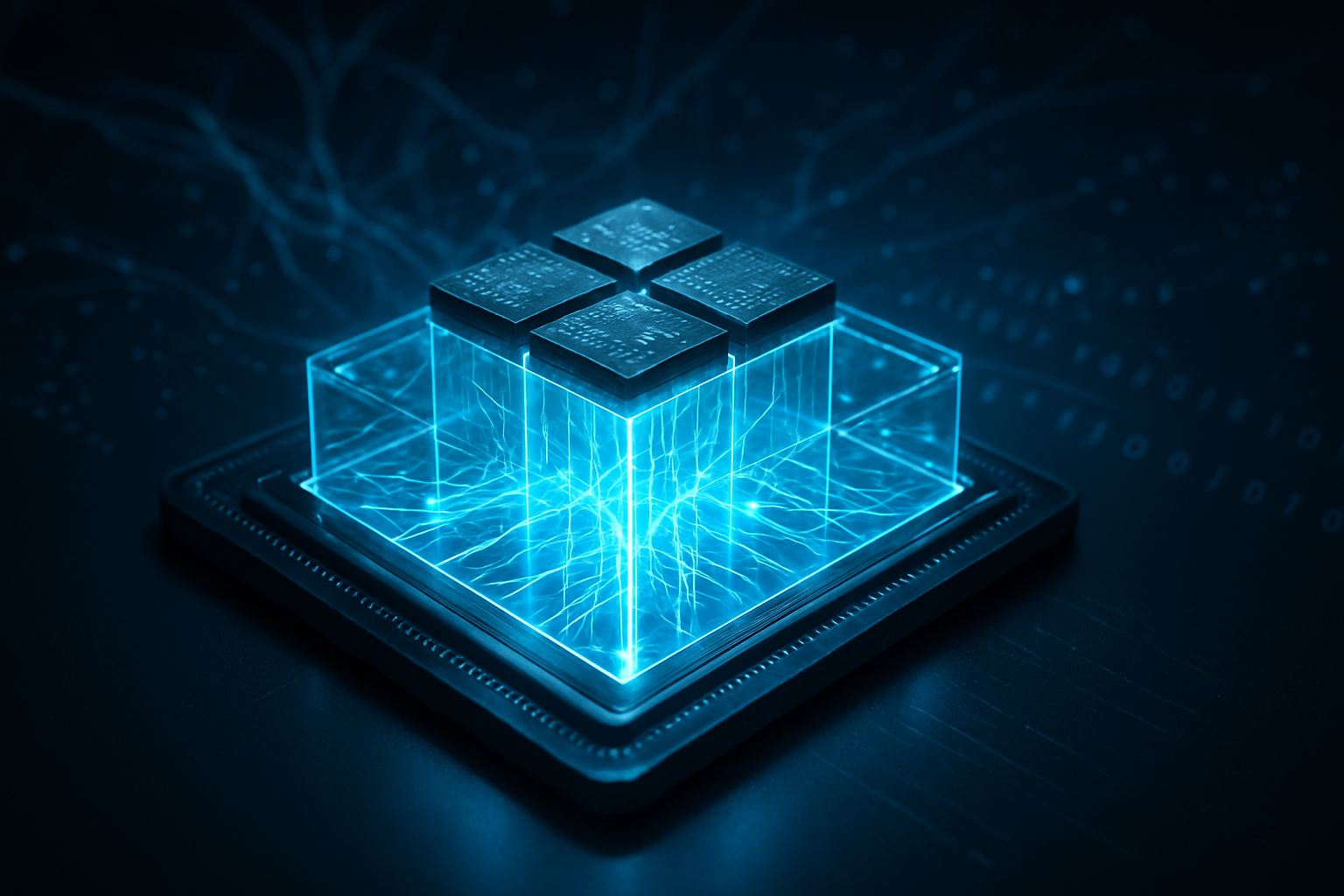
    The heart of this announcement is the transition from a GPU-centric model to a comprehensive "six-chip" unified platform. Central to this is the Rubin GPU (R200), a dual-die behemoth boasting 336 billion transistors—a 1.6x increase in density over its predecessor. This silicon giant delivers 50 Petaflops of NVFP4 compute performance. Complementing the GPU is the newly christened Vera CPU, NVIDIA’s first dedicated high-performance processor designed specifically for AI orchestration. Built on 88 custom "Olympus" ARM cores (v9.2-A), the Vera CPU utilizes spatial multi-threading to handle 176 concurrent threads, ensuring that the Rubin GPUs are never starved for data.

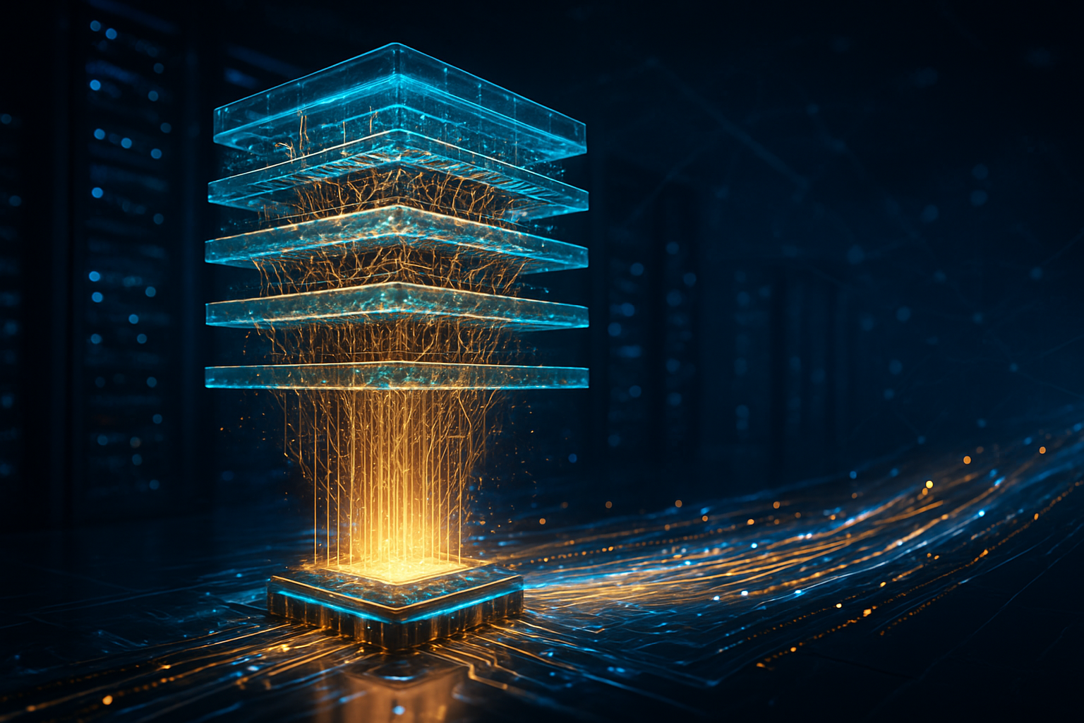
    To solve the perennial "memory wall" bottleneck, NVIDIA has fully embraced HBM4 memory. Each Rubin GPU features 288GB of HBM4, delivering an unprecedented 22 TB/s of memory bandwidth—a 2.8x jump over the Blackwell generation. This is coupled with the NVLink-C2C (Chip-to-Chip) interconnect, providing 1.8 TB/s of coherent bandwidth between the Vera CPU and Rubin GPUs. Rounding out the six-chip platform are the NVLink 6 Switch, the ConnectX-9 SuperNIC, the BlueField-4 DPU, and the Spectrum-6 Ethernet Switch, all designed to work in concert to eliminate latency in million-GPU clusters.

    The technical community has responded with a mix of awe and strategic caution. While the 3rd-generation Transformer Engine's hardware-accelerated adaptive compression is being hailed as a "game-changer" for Mixture-of-Experts (MoE) models, some researchers note that the sheer complexity of the rack-scale architecture will require a complete rethink of data center cooling and power delivery. The Rubin platform moves liquid cooling from an optional luxury to a mandatory standard, as the power density of these "AI factories" reaches new heights.

    Disruption in the Datacenter: Impact on Tech Giants and Competitors

    The unveiling of Rubin has immediate and profound implications for the world’s largest technology companies. Hyperscalers such as Microsoft (NASDAQ: MSFT), Alphabet (NASDAQ: GOOGL), and Amazon (NASDAQ: AMZN) have already announced massive procurement orders, with Microsoft’s upcoming "Fairwater" superfactories expected to be the first to deploy the Vera Rubin NVL72 rack systems. For these giants, the promised 10x reduction in inference costs is the key to moving their AI services from loss-leading experimental features to highly profitable enterprise utilities.

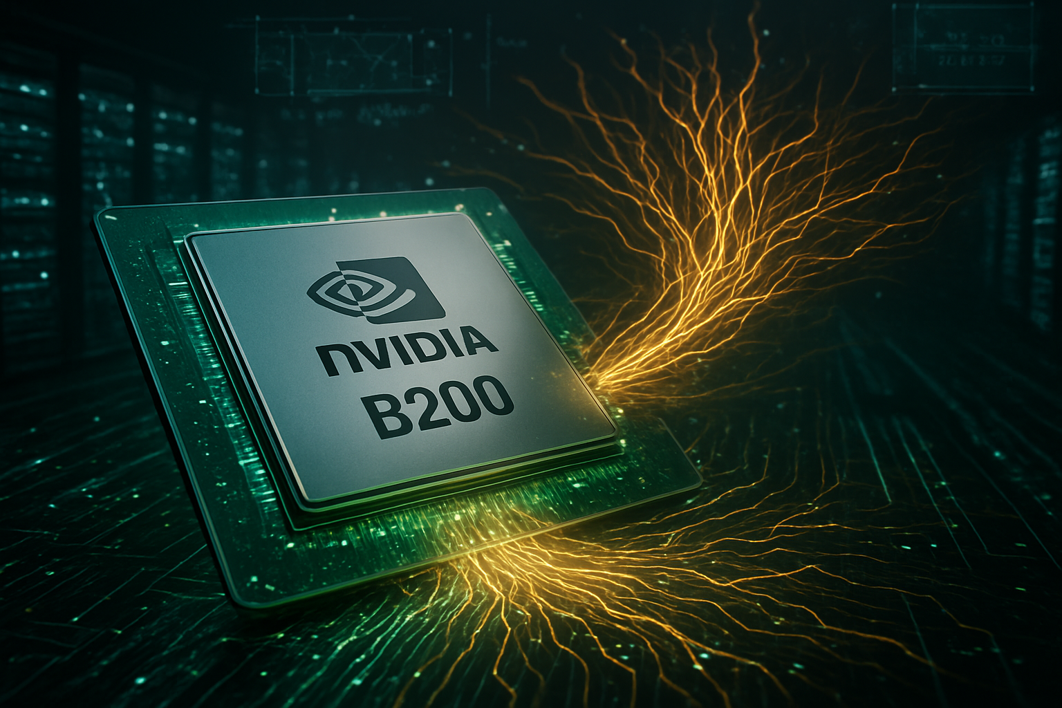
    For competitors like Advanced Micro Devices (NASDAQ: AMD), the Rubin announcement raises the stakes significantly. Industry analysts noted that NVIDIA’s decision to upgrade Rubin's memory bandwidth to 22 TB/s shortly before the CES reveal was a tactical maneuver to overshadow AMD’s Instinct MI455X. By offering a unified CPU-GPU-Networking stack, NVIDIA is increasingly positioning itself not just as a chip vendor, but as a vertically integrated platform provider, making it harder for "best-of-breed" component strategies from rivals to gain traction in the enterprise market.

    Furthermore, AI research labs like OpenAI and Anthropic are viewing Rubin as the necessary hardware "step-change" to enable agentic AI. OpenAI CEO Sam Altman, who made a guest appearance during the keynote, emphasized that the efficiency gains of Rubin are essential for scaling models that can perform long-context reasoning and maintain "memory" over weeks or months of user interaction. The strategic advantage for any lab securing early access to Rubin silicon in late 2026 could be the difference between a static chatbot and a truly autonomous digital employee.

    Sustainability and the Evolution of the AI Landscape

    Beyond the raw performance metrics, the Rubin architecture addresses the growing global concern regarding the energy consumption of AI. NVIDIA claims an 8x improvement in performance-per-watt over previous generations. This shift is critical as the world grapples with the power demands of the "AI revolution." By requiring 4x fewer GPUs to train the same MoE models compared to the Blackwell architecture, Rubin offers a path toward a more sustainable, if still power-hungry, future for digital intelligence.

    The move toward "agentic AI"—systems that can plan, reason, and execute complex tasks over long periods—is the primary trend driving this hardware evolution. Previously, the cost of keeping a high-reasoning model "active" for hours of thought was prohibitive. With Rubin, the cost per token drops so significantly that these "thinking" models can become ubiquitous. This follows the broader industry trend of moving away from simple prompt-response interactions toward continuous, collaborative AI workflows.

    However, the rapid pace of development has also sparked concerns about "hardware churn." With Blackwell only reaching volume production six months ago, the announcement of its successor has some enterprise buyers worried about the rapid depreciation of their current investments. NVIDIA’s aggressive roadmap—which includes a "Rubin Ultra" refresh already slated for 2027—suggests that the window for "cutting-edge" hardware is shrinking to a matter of months, forcing a cycle of constant reinvestment for those who wish to remain competitive in the AI arms race.

    Looking Ahead: The Road to Late 2026 and Beyond

    While the CES 2026 announcement provided the blueprint, the actual market rollout of the Rubin platform is scheduled for the second half of 2026. This timeline gives cloud providers and enterprises roughly nine months to prepare their infrastructure for the transition to HBM4 and the Vera CPU's ARM-based orchestration. In the near term, we can expect a flurry of software updates to CUDA and other NVIDIA libraries as the company prepares developers to take full advantage of the new NVLink 6 and 3rd-gen Transformer Engine.

    The long-term vision teased by Jensen Huang points toward the "Kyber" architecture in 2028, which is rumored to push rack-scale performance to 600kW. For now, the focus remains on the successful manufacturing of the Rubin R200 GPU. The complexity of the dual-die design and the integration of HBM4 will be the primary hurdles for NVIDIA’s supply chain. If successful, the Rubin architecture will likely be remembered as the moment AI hardware finally caught up to the ambitious dreams of software researchers, providing the raw power needed for truly autonomous intelligence.

    Summary of a Landmark Announcement

    The unveiling of the NVIDIA Rubin architecture at CES 2026 marks a definitive moment in tech history. By promising a 10x reduction in inference costs and delivering a tightly integrated six-chip platform, NVIDIA has consolidated its lead in the AI infrastructure market. The combination of the Vera CPU, the Rubin GPU, and HBM4 memory represents a fundamental redesign of how computers think, prioritizing the flow of data and the efficiency of reasoning over simple raw compute.

    As we move toward the late 2026 launch, the industry will be watching closely to see if NVIDIA can meet its ambitious production targets and if the 10x cost reduction translates into a new wave of AI-driven economic productivity. For now, the "Rubin Era" has officially begun, and the stakes for the future of artificial intelligence have never been higher.


    This content is intended for informational purposes only and represents analysis of current AI developments.

    TokenRing AI delivers enterprise-grade solutions for multi-agent AI workflow orchestration, AI-powered development tools, and seamless remote collaboration platforms.
    For more information, visit https://www.tokenring.ai/.

  • The 18A Era Begins: Intel Claims the Transistor Crown at CES 2026 with Panther Lake

    The 18A Era Begins: Intel Claims the Transistor Crown at CES 2026 with Panther Lake

    The Intel Corporation (NASDAQ: INTC) officially inaugurated the "18A Era" this month at CES 2026, launching its highly anticipated Core Ultra Series 3 processors, codenamed "Panther Lake." This launch marks more than just a seasonal hardware refresh; it represents the successful completion of CEO Pat Gelsinger’s audacious "five nodes in four years" (5N4Y) strategy, effectively signaling Intel’s return to the vanguard of semiconductor manufacturing.

    The arrival of Panther Lake is being hailed as the most significant milestone for the Silicon Valley giant in over a decade. By moving into high-volume manufacturing on the Intel 18A node, the company has delivered a product that promises to redefine the "AI PC" through unprecedented power efficiency and a massive leap in local processing capabilities. As of January 22, 2026, the tech industry is witnessing a fundamental shift in the competitive landscape as Intel moves to reclaim the title of the world’s most advanced chipmaker from rivals like TSMC (NYSE: TSM).

    Technical Breakthroughs: RibbonFET, PowerVia, and the 18A Architecture

    The Core Ultra Series 3 is the first consumer platform built on the Intel 18A (1.8nm-class) process, a node that introduces two revolutionary architectural changes: RibbonFET and PowerVia. RibbonFET is Intel’s implementation of Gate-All-Around (GAA) transistors, which replace the aging FinFET structure. This design allows for a multi-channel gate that surrounds the transistor channel on all sides, drastically reducing electrical leakage and allowing for finer control over performance and power consumption.

    Complementing this is PowerVia, Intel’s industry-first backside power delivery system. By moving the power routing to the reverse side of the silicon wafer, Intel has decoupled power delivery from data signaling. This separation solves the "voltage droop" issues that have plagued sub-3nm designs, resulting in a staggering 36% improvement in power efficiency at identical clock speeds compared to previous nodes. The top-tier Panther Lake SKUs feature a hybrid architecture of "Cougar Cove" Performance-cores and "Darkmont" Efficiency-cores, delivering a reported 60% leap in multi-threaded performance over the 2024-era Lunar Lake chips.

    Initial reactions from the AI research community have focused heavily on the integrated NPU 5 (Neural Processing Unit). Panther Lake’s dedicated AI silicon delivers 50 TOPS (Trillions of Operations Per Second) on its own, but when combined with the CPU and the new Xe3 "Celestial" integrated graphics, the total platform AI throughput reaches 180 TOPS. This capacity allows for the local execution of large language models (LLMs) that previously required cloud-based acceleration, a feat that industry experts suggest will fundamentally change how users interact with their operating systems and creative software.

    A Seismic Shift in the Competitive Landscape

    The successful rollout of 18A has immediate and profound implications for the entire semiconductor sector. For years, Advanced Micro Devices (NASDAQ: AMD) and Apple Inc. (NASDAQ: AAPL) enjoyed a manufacturing advantage by leveraging TSMC’s superior nodes. However, with TSMC’s N2 (2nm) process seeing slower-than-expected yields in early 2026, Intel has seized a narrow but critical window of "process leadership." This "leadership" isn't just about Intel’s own chips; it is the cornerstone of the Intel Foundry strategy.

    The market impact is already visible. Industry reports indicate that NVIDIA (NASDAQ: NVDA) has committed nearly $5 billion to reserve capacity on Intel’s 18A lines for its next-generation data center components, seeking to diversify its supply chain away from a total reliance on Taiwan. Meanwhile, AMD's upcoming "Zen 6" architecture is not expected to hit the mobile market in volume until late 2026 or early 2027, giving Intel a significant 9-to-12-month head start in the premium laptop and workstation segments.

    For startups and smaller AI labs, the proliferation of 180-TOPS consumer hardware lowers the barrier to entry for "Edge AI" applications. Developers can now build sophisticated, privacy-centric AI tools that run entirely on a user's laptop, bypassing the high costs and latency of centralized APIs. This shift threatens the dominance of cloud-only AI providers by moving the "intelligence" back to the local device.

    The Geopolitical and Philosophical Significance of 18A

    Beyond benchmarks and market share, the 18A milestone is a victory for the "Silicon Shield" strategy in the West. As the first leading-edge node to be manufactured in significant volumes on U.S. soil, 18A represents a critical step toward rebalancing the global semiconductor supply chain. This development fits into the broader trend of "techno-nationalism," where the ability to manufacture the world's fastest transistors is seen as a matter of national security as much as economic prowess.

    However, the rapid advancement of local AI capabilities also raises concerns. With Panther Lake making high-performance AI accessible to hundreds of millions of consumers, the industry faces renewed questions regarding deepfakes, local data privacy, and the environmental impact of keeping "AI-always-on" hardware in every home. While Intel claims a record 27 hours of battery life for Panther Lake reference designs, the aggregate energy consumption of an AI-saturated PC market remains a topic of debate among sustainability advocates.

    Comparatively, the move to 18A is being likened to the transition from vacuum tubes to integrated circuits. It is a "once-in-a-generation" architectural pivot. While previous nodes focused on incremental shrinks, 18A's combination of backside power and GAA transistors represents a fundamental redesign of how electricity moves through silicon, potentially extending the life of Moore’s Law for another decade.

    The Horizon: From Panther Lake to 14A and Beyond

    Looking ahead, Intel's roadmap does not stop at 18A. The company is already touting the development of the Intel 14A node, which is expected to integrate High-NA EUV (Extreme Ultraviolet) lithography more extensively. Near-term, the focus will shift from consumer laptops to the data center with "Clearwater Forest," a Xeon processor built on 18A that aims to challenge the dominance of ARM-based server chips in the cloud.

    Experts predict that the next two years will see a "Foundry War" as TSMC ramps up its own backside power delivery systems to compete with Intel's early-mover advantage. The primary challenge for Intel now is maintaining these yields as production scales from millions to hundreds of millions of units. Any manufacturing hiccups in the next six months could give rivals an opening to close the gap.

    Furthermore, we expect to see a surge in "Physical AI" applications. With Panther Lake being certified for industrial and robotics use cases at launch, the 18A architecture will likely find its way into autonomous delivery drones, medical imaging devices, and advanced manufacturing bots by the end of 2026.

    A Turnaround Validated: Final Assessment

    The launch of Core Ultra Series 3 at CES 2026 is the ultimate validation of Pat Gelsinger’s "Moonshot" for Intel. By successfully executing five process nodes in four years, the company has transformed itself from a struggling incumbent into a formidable manufacturing powerhouse once again. The 18A node is the physical manifestation of this turnaround—a technological marvel that combines RibbonFET and PowerVia to reclaim the top spot in the semiconductor hierarchy.

    Key takeaways for the industry are clear: Intel is no longer "chasing" the leaders; it is setting the pace. The immediate availability of Panther Lake on January 27, 2026, will be the true test of this new era. Watch for the first wave of third-party benchmarks and the subsequent quarterly earnings from Intel and its foundry customers to see if the "18A Era" translates into the financial resurgence the company has promised.

    For now, the message from CES is undeniable: the race for the next generation of computing has a new frontrunner, and it is powered by 1.8nm silicon.


    This content is intended for informational purposes only and represents analysis of current AI developments.

    TokenRing AI delivers enterprise-grade solutions for multi-agent AI workflow orchestration, AI-powered development tools, and seamless remote collaboration platforms.
    For more information, visit https://www.tokenring.ai/.

  • AMD’s Ryzen AI 400 Series Debuts at CES 2026: The New Standard for On-Device Sovereignty

    AMD’s Ryzen AI 400 Series Debuts at CES 2026: The New Standard for On-Device Sovereignty

    At the 2026 Consumer Electronics Show (CES) in Las Vegas, Advanced Micro Devices, Inc. (NASDAQ: AMD) officially unveiled its Ryzen AI 400 series, a breakthrough in the evolution of the “AI PC” that transitions local artificial intelligence from a luxury feature to a mainstream necessity. Codenamed "Gorgon Point," the new silicon lineup introduces the industry’s first dedicated Copilot+ desktop processors and sets a new benchmark for on-device inference efficiency. By pushing the boundaries of neural processing power, AMD is making a bold claim: the future of high-end AI development and execution no longer belongs solely to the cloud or massive server racks, but to the laptop on your desk.

    The announcement marks a pivotal shift in the hardware landscape, as AMD moves beyond the niche adoption of early AI accelerators toward a "volume platform" strategy. The Ryzen AI 400 series aims to solve the latency and privacy bottlenecks that have historically plagued cloud-dependent AI services. With significant gains in NPU (Neural Processing Unit) throughput and a specialized "Halo" platform designed for extreme local workloads, AMD is positioning itself as the leader in "Sovereign AI"—the ability for individuals and enterprises to run massive, complex models entirely offline without sacrificing performance or battery life.

    Technical Prowess: 60 TOPS and the 200-Billion Parameter Local Frontier

    The Ryzen AI 400 series is built on a refined second-generation XDNA 2 architecture, paired with the proven Zen 5 and Zen 5c CPU cores on a TSMC (NYSE: TSM) 4nm process. The flagship of the mobile lineup, the Ryzen AI 9 HX 475, delivers an industry-leading 60 NPU TOPS (Trillions of Operations Per Second). This is a 20% jump over the previous generation and comfortably exceeds the 40 TOPS requirement set by Microsoft Corporation (NASDAQ: MSFT) for the Copilot+ ecosystem. To support this massive compute capability, AMD has upgraded memory support to LPDDR5X-8533 MT/s, ensuring that the high-speed data paths required for real-time generative AI remain clear and responsive.

    While the standard 400 series caters to everyday productivity and creative tasks, the real showstopper at CES was the "Ryzen AI Halo" platform, utilizing the Ryzen AI Max+ silicon. In a live demonstration that stunned the audience, AMD showed the Halo platform running a 200-billion parameter large language model (LLM) locally. This feat, previously thought impossible for a consumer-grade workstation without multiple dedicated enterprise GPUs, is made possible by 128GB of high-speed unified memory. This allows the processor to handle massive datasets and complex reasoning tasks that were once the sole domain of data centers.

    This technical achievement differs significantly from previous approaches, which relied on "quantization"—the process of shrinking models and losing accuracy to fit them onto consumer hardware. The Ryzen AI 400 series, particularly in its Max+ configuration, provides enough raw bandwidth and specialized NPU cycles to run high-fidelity models. Initial reactions from the AI research community have been overwhelmingly positive, with many experts noting that this level of local compute could democratize AI research, allowing developers to iterate on sophisticated models without the mounting costs of cloud API tokens.

    Market Warfare: The Battle for the AI PC Crown

    The introduction of the Ryzen AI 400 series intensifies a three-way battle for dominance in the 2026 hardware market. While Intel Corporation (NASDAQ: INTC) used CES to showcase its "Panther Lake" architecture, focusing on a 50% improvement in power efficiency and its new Xe3 "Battlemage" graphics, AMD’s strategy leans more heavily into raw AI performance and "unplugged" consistency. AMD claims a 70% improvement in performance-per-watt while running on battery compared to its predecessor, directly challenging the efficiency narrative long held by Apple and ARM-based competitors.

    Qualcomm Incorporated (NASDAQ: QCOM) remains a formidable threat with its Snapdragon X2 Elite, which currently leads the market in raw NPU metrics at 80 TOPS. However, AMD’s strategic advantage lies in its x86 legacy. By bringing Copilot+ capabilities to the desktop for the first time with the Ryzen AI 400 series, AMD is securing the enterprise sector, where compatibility with legacy software and high-performance desktop workflows remains non-negotiable. This move effectively boxes out competitors who are still struggling to translate ARM efficiency into the heavy-duty desktop market.

    The "Ryzen AI Max+" also represents a direct challenge to NVIDIA Corporation (NASDAQ: NVDA) and its dominance in the AI workstation market. By offering a unified chip that can handle both traditional compute and massive AI inference, AMD is attempting to lure developers into its ROCm (Radeon Open Compute) software ecosystem. If AMD can convince the next generation of AI engineers that they can build, test, and deploy 200B parameter models on a single Ryzen AI-powered machine, it could significantly disrupt the sales of entry-level enterprise AI GPUs.

    A Cultural Shift Toward AI Sovereignty and Privacy

    Beyond the raw specifications, the Ryzen AI 400 series reflects a broader trend in the tech industry: the move toward "Sovereign AI." As concerns over data privacy, cloud security, and the environmental cost of massive data centers grow, the ability to process data locally is becoming a major selling point. For industries like healthcare, law, and finance—where data cannot leave the local network for regulatory reasons—AMD’s new chips provide a path to utilize high-end generative AI without the risks associated with third-party cloud providers.

    This development follows the trajectory of the "AI PC" evolution that began in late 2023 but finally reached maturity in 2026. Earlier milestones were focused on simple background blur for video calls or basic text summarization. The 400 series, however, enables "high-level reasoning" locally. This means a laptop can now serve as a truly autonomous digital twin, capable of managing complex schedules, coding entire applications, and analyzing massive spreadsheets without ever sending a packet of data to the internet.

    Potential concerns remain, particularly regarding the "AI tax" on hardware prices. As NPUs become larger and memory requirements skyrocket to support 128GB unified architectures, the cost of top-tier AI laptops is expected to rise. Furthermore, the software ecosystem must keep pace; while the hardware is now capable of running 200B parameter models, the user experience depends entirely on how effectively developers can optimize their software to leverage AMD’s XDNA 2 architecture.

    The Horizon: What Comes After 60 TOPS?

    Looking ahead, the Ryzen AI 400 series is just the beginning of a multi-year roadmap for AMD. Industry analysts predict that by 2027, we will see the introduction of "XDNA 3" and "Zen 6" architectures, which are expected to push NPU performance beyond the 100 TOPS mark for mobile devices. Near-term developments will likely focus on the "Ryzen AI Software" suite, with AMD expected to release more robust tools for one-click local LLM deployment, making it easier for non-technical users to host their own private AI assistants.

    The potential applications are vast. In the coming months, we expect to see the rise of "Personalized Local LLMs"—AI models that are fine-tuned on a user’s specific files, emails, and voice recordings, stored and processed entirely on their Ryzen AI 400 device. Challenges remain in cooling these high-performance NPUs in thin-and-light chassis, but AMD’s move to a 4nm process and focus on "sustained unplugged performance" suggests they have a significant lead in managing the thermal realities of mobile AI.

    Final Assessment: A Landmark Moment for Computing

    The unveiling of the Ryzen AI 400 series at CES 2026 will likely be remembered as the moment the "AI PC" became a reality for the masses. By standardizing 60 TOPS across its stack and providing a "Halo" tier capable of running world-class AI models locally, AMD has redefined the expectations for personal computing. This isn't just a spec bump; it is a fundamental reconfiguration of where intelligence lives in the digital age.

    The significance of this development in AI history cannot be overstated. We are moving from an era of "Cloud-First" AI to "Local-First" AI. In the coming weeks, as the first laptops featuring the Ryzen AI 9 HX 475 hit the shelves, the tech world will be watching closely to see if real-world performance matches the impressive CES benchmarks. If AMD’s promises of 24-hour battery life and 200B parameter local inference hold true, the balance of power in the semiconductor industry may have just shifted permanently.


    This content is intended for informational purposes only and represents analysis of current AI developments.

    TokenRing AI delivers enterprise-grade solutions for multi-agent AI workflow orchestration, AI-powered development tools, and seamless remote collaboration platforms.
    For more information, visit https://www.tokenring.ai/.

  • The Dawn of the Physical AI Era: Silicon Titans Redefine CES 2026

    The Dawn of the Physical AI Era: Silicon Titans Redefine CES 2026

    The recently concluded CES 2026 in Las Vegas will be remembered as the moment the artificial intelligence revolution stepped out of the chat box and into the physical world. Officially heralded as the "Year of Physical AI," the event marked a historic pivot from the generative text and image models of 2024–2025 toward embodied systems that can perceive, reason, and act within our three-dimensional environment. This shift was underscored by a massive coordinated push from the world’s leading semiconductor manufacturers, who unveiled a new generation of "Physical AI" processors designed to power everything from "Agentic PCs" to fully autonomous humanoid robots.

    The significance of this year’s show lies in the maturation of edge computing. For the first time, the industry demonstrated that the massive compute power required for complex reasoning no longer needs to reside exclusively in the cloud. With the launch of ultra-high-performance NPUs (Neural Processing Units) from the industry's "Four Horsemen"—Nvidia, Intel, AMD, and Qualcomm—the promise of low-latency, private, and physically capable AI has finally moved from research prototypes to mass-market production.

    The Silicon War: Specs of the 'Four Horsemen'

    The technological centerpiece of CES 2026 was the "four-way war" in AI silicon. Nvidia (NASDAQ:NVDA) set the pace early by putting its "Rubin" architecture into full production. CEO Jensen Huang declared a "ChatGPT moment for robotics" as he unveiled the Jetson T4000, a Blackwell-powered module delivering a staggering 1,200 FP4 TFLOPS. This processor is specifically designed to be the "brain" of humanoid robots, supported by Project GR00T and Cosmos, an "open world foundation model" that allows machines to learn motor tasks from video data rather than manual programming.

    Not to be outdone, Intel (NASDAQ:INTC) utilized the event to showcase the success of its turnaround strategy with the official launch of Panther Lake (Core Ultra Series 3). Manufactured on the cutting-edge Intel 18A process node, the chip features the new NPU 5, which delivers 50 TOPS locally. Intel’s focus is the "Agentic AI PC"—a machine capable of managing a user’s entire digital life and local file processing autonomously. Meanwhile, Qualcomm (NASDAQ:QCOM) flexed its efficiency muscles with the Snapdragon X2 Elite Extreme, boasting an 18-core Oryon 3 CPU and an 80 TOPS NPU. Qualcomm also introduced the Dragonwing IQ10, a dedicated platform for robotics that emphasizes power-per-watt, enabling longer battery life for mobile humanoids like the Vinmotion Motion 2.

    AMD (NASDAQ:AMD) rounded out the quartet by bridging the gap between the data center and the desktop. Their new Ryzen AI "Gorgon Point" series features an expanded matrix engine and the first native support for "Copilot+ Desktop" high-performance workloads. AMD also teased its Helios platform, a rack-scale solution powered by Zen 6 EPYC "Venice" processors, intended to train the very physical world models that the smaller Ryzen chips execute at the edge. Industry experts have noted that while previous years focused on software breakthroughs, 2026 is defined by the hardware's ability to handle "multimodal reasoning"—the ability for a device to see an object, understand its physical properties, and decide how to interact with it in real-time.

    Market Maneuvers: From Cloud Dominance to Edge Supremacy

    This shift toward Physical AI is fundamentally reshaping the competitive landscape of the tech industry. For years, the AI narrative was dominated by cloud providers and LLM developers. However, CES 2026 proved that the "edge"—the devices we carry and the robots that work alongside us—is the new battleground for strategic advantage. Nvidia is positioning itself as the "Infrastructure King," providing not just the chips but the entire software stack (Omniverse and Isaac) needed to simulate and train physical entities. By owning the simulation environment, Nvidia seeks to make its hardware the indispensable foundation for every robotics startup.

    In contrast, Qualcomm and Intel are targeting the "volume market." Qualcomm is leveraging its heritage in mobile connectivity to dominate "connected robotics," where 5G and 6G integration are vital for warehouse automation and consumer bots. Intel, through its 18A manufacturing breakthrough, is attempting to reclaim the crown of the "PC Brain" by making AI features so deeply integrated into the OS that a cloud connection becomes optional. Startups like Boston Dynamics (backed by Hyundai and Google DeepMind) and Vinmotion are the primary beneficiaries of this rivalry, as the sudden abundance of high-performance, low-power silicon allows them to transition from experimental models to production-ready units capable of "human-level" dexterity.

    The competitive implications extend beyond silicon. Tech giants are now forced to choose between "walled garden" AI ecosystems or open-source Physical AI frameworks. The move toward local processing also threatens the dominance of current subscription-based AI models; if a user’s Intel-powered laptop or Qualcomm-powered robot can perform complex reasoning locally, the strategic advantage of centralized AI labs like OpenAI or Anthropic could begin to erode in favor of hardware-software integrated giants.

    The Wider Significance: When AI Gets a Body

    The transition from "Digital AI" to "Physical AI" represents a profound milestone in human-computer interaction. For the first time, the "hallucinations" that plagued early generative AI have moved from being a nuisance in text to a safety critical engineering challenge. At CES 2026, panels featuring leaders from Siemens and Mercedes-Benz emphasized that "Physical AI" requires "error intolerance." A robot navigating a crowded home or a factory floor cannot afford a single reasoning error, leading to the introduction of "safety-grade" silicon architectures that partition AI logic from critical motor controls.

    This development also brings significant societal concerns to the forefront. As AI becomes embedded in physical infrastructure—from elevators that predict maintenance to autonomous industrial helpers—the question of accountability becomes paramount. Experts at the event raised alarms regarding "invisible AI," where autonomous systems become so pervasive that their decision-making processes are no longer transparent to the humans they serve. The industry is currently racing to establish "document trails" for AI reasoning to ensure that when a physical system fails, the cause can be diagnosed with the same precision as a mechanical failure.

    Comparatively, the 2023 generative AI boom was about "creation," while the 2026 Physical AI breakthrough is about "utility." We are moving away from AI as a toy or a creative partner and toward AI as a functional laborer. This has reignited debates over labor displacement, but with a new twist: the focus is no longer just on white-collar "knowledge work," but on blue-collar tasks in logistics, manufacturing, and elder care.

    Beyond the Horizon: The 2027 Roadmap

    Looking ahead, the momentum generated at CES 2026 shows no signs of slowing. Near-term developments will likely focus on the refinement of "Agentic AI PCs," where the operating system itself becomes a proactive assistant that performs tasks across different applications without user prompting. Long-term, the industry is already looking toward 2027, with Intel teasing its Nova Lake architecture (rumored to feature 52 cores) and AMD preparing its Medusa (Zen 6) chips based on TSMC’s 2nm process. These upcoming iterations aim to bring even more "brain-like" density to consumer hardware.

    The next major challenge for the industry will be the "sim-to-real" gap—the difficulty of taking an AI trained in a virtual simulation and making it function perfectly in the messy, unpredictable real world. Future applications on the horizon include "personalized robotics," where robots are not just general-purpose tools but are fine-tuned to the specific layout and needs of an individual's home. Predictably, experts believe the next 18 months will see a surge in M&A activity as silicon giants move to acquire robotics software startups to complete their "Physical AI" portfolios.

    The Wrap-Up: A Turning Point in Computing History

    CES 2026 has served as a definitive declaration that the "post-chat" era of artificial intelligence has arrived. The key takeaways from the event are clear: the hardware has finally caught up to the software, and the focus of innovation has shifted from virtual outputs to physical actions. The coordinated launches from Nvidia, Intel, AMD, and Qualcomm have provided the foundation for a world where AI is no longer a guest on our screens but a participant in our physical spaces.

    In the history of AI, 2026 will likely be viewed as the year the technology gained its "body." As we look toward the coming months, the industry will be watching closely to see how these new processors perform in real-world deployments and how consumers react to the first wave of truly autonomous "Agentic" devices. The silicon war is far from over, but the battlefield has officially moved into the real world.


    This content is intended for informational purposes only and represents analysis of current AI developments.

    TokenRing AI delivers enterprise-grade solutions for multi-agent AI workflow orchestration, AI-powered development tools, and seamless remote collaboration platforms.
    For more information, visit https://www.tokenring.ai/.

  • The Silicon Soul: Why 2026 is the Definitive Year of Physical AI and the Edge Revolution

    The Silicon Soul: Why 2026 is the Definitive Year of Physical AI and the Edge Revolution

    The dust has settled on CES 2026, and the verdict from the tech industry is unanimous: we have officially entered the Year of Physical AI. For the past three years, artificial intelligence was largely a "cloud-first" phenomenon—a digital brain trapped in a data center, accessible only via an internet connection. However, the announcements in Las Vegas this month have signaled a tectonic shift. AI has finally moved from the server rack to the "edge," manifesting in hardware that can perceive, reason about, and interact with the physical world in real-time, without a single byte leaving the local device.

    This "Edge AI Revolution" is powered by a new generation of silicon that has turned the personal computer into an "AI Hub." With the release of groundbreaking hardware from industry titans like Intel (NASDAQ:INTC) and Qualcomm (NASDAQ:QCOM), the 2026 hardware landscape is defined by its ability to run complex, multi-modal local agents. These are not mere chatbots; they are proactive systems capable of managing entire digital and physical workflows. The era of "AI-as-a-service" is being challenged by "AI-as-an-appliance," bringing unprecedented privacy, speed, and autonomy to the average consumer.

    The 100 TOPS Milestone: Under the Hood of the 2026 AI PC

    The technical narrative of 2026 is dominated by the race for Neural Processing Unit (NPU) supremacy. At the heart of this transition is Intel’s Panther Lake (Core Ultra Series 3), which officially launched at CES 2026. Built on the cutting-edge Intel 18A process, Panther Lake features the new NPU 5 architecture, delivering a dedicated 50 TOPS (Tera Operations Per Second). When paired with the integrated Arc Xe3 "Celestial" graphics, the total platform performance reaches a staggering 170 TOPS. This allows laptops to perform complex video editing and local 3D rendering that previously required a dedicated desktop GPU.

    Not to be outdone, Qualcomm (NASDAQ:QCOM) showcased the Snapdragon X2 Elite Extreme, specifically designed for the next generation of Windows on Arm. Its Hexagon NPU 6 achieves a massive 85 TOPS, setting a new benchmark for dedicated NPU performance in ultra-portable devices. Even more impressive was the announcement of the Snapdragon 8 Elite Gen 5 for mobile devices, which became the first mobile chipset to hit the 100 TOPS NPU milestone. This level of local compute power allows "Small Language Models" (SLMs) to run at speeds exceeding 200 tokens per second, enabling real-time, zero-latency voice and visual interaction.

    This represents a fundamental departure from the 2024 era of AI PCs. While early devices like those powered by the original Lunar Lake or Snapdragon X Elite could handle basic background blurring and text summarization, the 2026 class of hardware can host "Agentic AI." These systems utilize local "world models"—AI that understands physical constraints and cause-and-effect—allowing them to control robotics or manage complex multi-app tasks locally. Industry experts note that the 100 TOPS threshold is the "magic number" required for AI to move from passive response to active agency.

    The Battle for the Edge: Market Implications and Strategic Shifts

    The shift toward edge-based Physical AI has created a high-stakes battleground for silicon supremacy. Intel (NASDAQ:INTC) is leveraging its 18A manufacturing process to prove it can out-innovate competitors in both design and fabrication. By hitting the 50 TOPS NPU floor across its entire consumer line, Intel is forcing a rapid obsolescence of non-AI hardware, effectively mandating a global PC refresh cycle. Meanwhile, Qualcomm (NASDAQ:QCOM) is tightening its grip on the high-efficiency laptop market, challenging Apple (NASDAQ:AAPL) for the title of best performance-per-watt in the mobile computing space.

    This revolution also poses a strategic threat to traditional cloud providers like Alphabet (NASDAQ:GOOGL) and Amazon (NASDAQ:AMZN). As more AI processing moves to the device, the reliance on expensive cloud inference is diminishing for standard tasks. Microsoft (NASDAQ:MSFT) has recognized this shift by launching the "Agent Hub" for Windows, an OS-level orchestration layer that allows local agents to coordinate tasks. This move ensures that even as AI becomes local, Microsoft remains the dominant platform for its execution.

    The robotics sector is perhaps the biggest beneficiary of this edge computing surge. At CES 2026, NVIDIA (NASDAQ:NVDA) solidified its lead in Physical AI with the Vera Rubin architecture and the Cosmos reasoning model. By providing the "brains" for companies like LG (KRX:066570) and Hyundai (OTC:HYMTF), NVIDIA is positioning itself as the foundational layer of the robotics economy. The market is shifting from "software-only" AI startups to those that can integrate AI into physical hardware, marking a return to tangible, product-based innovation.

    Beyond the Screen: Privacy, Latency, and the Physical AI Landscape

    The emergence of "Physical AI" addresses the two greatest hurdles of the previous AI era: privacy and latency. In 2026, the demand for Sovereign AI—the ability for individuals and corporations to own and control their data—has hit an all-time high. Local execution on NPUs means that sensitive data, such as a user’s calendar, private messages, and health data, never needs to be uploaded to a third-party server. This has opened the door for highly personalized agents like Lenovo’s (HKG:0992) "Qira," which indexes a user’s entire digital life locally to provide proactive assistance without compromising privacy.

    The latency improvements of 2026 hardware are equally transformative. For Physical AI—such as LG’s CLOiD home robot or the electric Atlas from Boston Dynamics—sub-millisecond reaction times are a necessity, not a luxury. By processing sensory input locally, these machines can navigate complex environments and interact with humans safely. This is a significant milestone compared to early cloud-dependent robots that were often hampered by "thinking" delays.

    However, this rapid advancement is not without its concerns. The "Year of Physical AI" brings new challenges regarding the safety and ethics of autonomous physical agents. If a local AI agent can independently book travel, manage bank accounts, or operate heavy machinery in a home or factory, the potential for hardware-level vulnerabilities becomes a physical security risk. Governments and regulatory bodies are already pivoting their focus from "content moderation" to "robotic safety standards," reflecting the shift from digital to physical AI impacts.

    The Horizon: From AI PCs to Zero-Labor Environments

    Looking beyond 2026, the trajectory of Edge AI points toward "Zero-Labor" environments. Intel has already teased its Nova Lake architecture for 2027, which is expected to be the first x86 chip to reach 100 TOPS on the NPU alone. This will likely make sophisticated local AI agents a standard feature even in budget-friendly hardware. We are also seeing the early stages of a unified "Agentic Ecosystem," where your smartphone, PC, and home robots share a local intelligence mesh, allowing them to pass tasks between one another seamlessly.

    Future applications currently on the horizon include "Ambient Computing," where the AI is no longer something you interact with through a screen, but a layer of intelligence that exists in the environment itself. Experts predict that by 2028, the concept of a "Personal AI Agent" will be as ubiquitous as the smartphone is today. These agents will be capable of complex reasoning, such as negotiating bills on your behalf or managing home energy systems to optimize for both cost and carbon footprint, all while running on local, renewable-powered edge silicon.

    A New Chapter in the History of Computing

    The "Year of Physical AI" will be remembered as the moment AI became truly useful for the average person. It is the year we moved past the novelty of generative text and into the utility of agentic action. The Edge AI revolution, spearheaded by the incredible engineering of 2026 silicon, has decentralized intelligence, moving it out of the hands of a few cloud giants and back onto the devices we carry and the machines we live with.

    The key takeaway from CES 2026 is that the hardware has finally caught up to the software's ambition. As we look toward the rest of the year, watch for the rollout of "Agentic" OS updates and the first true commercial deployment of household humanoid assistants. The "Silicon Soul" has arrived, and it lives locally.


    This content is intended for informational purposes only and represents analysis of current AI developments.

    TokenRing AI delivers enterprise-grade solutions for multi-agent AI workflow orchestration, AI-powered development tools, and seamless remote collaboration platforms.
    For more information, visit https://www.tokenring.ai/.

  • The Glass Age: Intel Debuts Xeon 6+ ‘Clearwater Forest’ at CES 2026 as First Mass-Produced Chip with Glass Core

    The Glass Age: Intel Debuts Xeon 6+ ‘Clearwater Forest’ at CES 2026 as First Mass-Produced Chip with Glass Core

    The semiconductor industry reached a historic inflection point this month at CES 2026, as Intel (NASDAQ: INTC) officially unveiled the Xeon 6+ 'Clearwater Forest' processor. This launch marks the world’s first successful high-volume implementation of glass core substrates in a commercial CPU, signaling the beginning of what engineers are calling the "Glass Age" of computing. By replacing traditional organic resin substrates with glass, Intel has effectively bypassed the "Warpage Wall" that has threatened to stall chip performance gains as AI-driven packages grow to unprecedented sizes.

    The transition to glass substrates is not merely a material change; it is a fundamental shift in how complex silicon systems are built. As artificial intelligence models demand exponentially more compute density and better thermal management, the industry’s reliance on organic materials like Ajinomoto Build-up Film (ABF) has reached its physical limit. The introduction of Clearwater Forest proves that glass is no longer a laboratory curiosity but a viable, mass-producible solution for the next generation of hyperscale data centers.

    Breaking the Warpage Wall: Technical Specifications of Clearwater Forest

    Intel's Xeon 6+ 'Clearwater Forest' is a marvel of heterogenous integration, utilizing the company’s cutting-edge Intel 18A process node for its compute tiles. The processor features up to 288 "Darkmont" Efficiency-cores (E-cores) per socket, enabling a staggering 576-core configuration in dual-socket systems. While the core count itself is impressive, the true innovation lies in the packaging. By utilizing glass substrates, Intel has achieved a 10x increase in interconnect density through laser-etched Through-Glass Vias (TGVs). These vias allow for significantly tighter routing between tiles, drastically reducing signal loss and improving power delivery efficiency by up to 50% compared to previous generations.

    The technical superiority of glass stems from its physical properties. Unlike organic substrates, which have a high coefficient of thermal expansion (CTE) that causes them to warp under the intense heat of modern AI workloads, glass can be engineered to match the CTE of silicon perfectly. This stability allows Intel to create "reticle-busting" packages that exceed 100mm x 100mm without the risk of the chip cracking or disconnecting from the board. Furthermore, the ultra-flat surface of glass—with sub-1nm roughness—enables superior lithographic focus, allowing for finer circuit patterns that were previously impossible to achieve on uneven organic resins.

    Initial reactions from the research community have been overwhelmingly positive. The Interuniversity Microelectronics Centre (IMEC) described the launch as a "paradigm shift," noting that the industry is moving from a chip-centric design model to a materials-science-centric one. By integrating Foveros Direct 3D stacking with EMIB 2.5D interconnects on a glass core, Intel has effectively built a "System-on-Package" that functions with the low latency of a single piece of silicon but the modularity of a modern disaggregated architecture.

    A New Battlefield: Market Positioning and the 'Triple Alliance'

    The debut of Clearwater Forest places Intel (NASDAQ: INTC) in a unique leadership position within the advanced packaging market, but the competition is heating up rapidly. Samsung Electro-Mechanics (KRX: 009150) has responded by mobilizing a "Triple Alliance"—a vertically integrated consortium including Samsung Display and Samsung Electronics—to fast-track its own glass substrate roadmap. While Intel currently holds the first-mover advantage, Samsung has announced it will begin full-scale validation and targets mass production for the second half of 2026. Samsung’s pilot line in Sejong, South Korea, is already reportedly producing samples for major mobile and AI chip designers.

    The competitive landscape is also seeing a shift in how major AI labs and cloud providers source their hardware. Companies like Amazon (NASDAQ: AMZN) and Google (NASDAQ: GOOGL) are increasingly looking for foundries that can handle the extreme thermal and electrical demands of their custom AI accelerators. Intel’s ability to offer glass-based packaging through its Intel Foundry (IFS) services makes it an attractive alternative to TSMC (NYSE: TSM). While TSMC remains the dominant force in traditional silicon-on-wafer packaging, its "CoPoS" (Chip-on-Panel-on-Substrate) glass technology is not expected to reach mass production until late 2028, potentially giving Intel a multi-year window to capture high-end AI market share.

    Furthermore, SK Hynix (KRX: 000660), through its subsidiary Absolics, is nearing the completion of its $300 million glass substrate facility in Georgia, USA. Absolics is specifically targeting the AI GPU market, with rumors suggesting that AMD (NASDAQ: AMD) is already testing glass-core prototypes for its next-generation Instinct accelerators. This fragmentation suggests that while Intel owns the CPU narrative today, the "Glass Age" will soon be a multi-vendor environment where specialized packaging becomes the primary differentiator between competing AI "superchips."

    Beyond Moore's Law: The Wider Significance for AI

    The transition to glass substrates is widely viewed as a necessary evolution to keep Moore’s Law alive in the era of generative AI. As LLMs (Large Language Models) grow in complexity, the chips required to train them are becoming physically larger, drawing more power and generating more heat. Standard organic packaging has become a bottleneck, often failing at power levels exceeding 1,000 watts. Glass, with its superior thermal stability and electrical insulation properties, allows for chips that can safely operate at higher temperatures and power densities, facilitating the continued scaling of AI compute.

    Moreover, this shift addresses the critical issue of data movement. In modern AI clusters, the "memory wall"—the speed at which data can travel between the processor and memory—is a primary constraint. Glass substrates enable much denser integration of High Bandwidth Memory (HBM), placing it closer to the compute cores than ever before. This proximity reduces the energy required to move data, which is essential for reducing the massive carbon footprint of modern AI data centers.

    Comparisons are already being drawn to the transition from aluminum to copper interconnects in the late 1990s—a move that similarly unlocked a decade of performance gains. The consensus among industry experts is that glass substrates are not just an incremental upgrade but a foundational requirement for the "Systems-on-Package" that will drive the AI breakthroughs of the late 2020s. However, concerns remain regarding the fragility of glass during the manufacturing process and the need for entirely new supply chains, as the industry pivots away from the organic materials it has relied on for thirty years.

    The Horizon: Co-Packaged Optics and Future Applications

    Looking ahead, the potential applications for glass substrates extend far beyond CPUs and GPUs. One of the most anticipated near-term developments is the integration of co-packaged optics (CPO). Because glass is transparent and can be precisely machined, it is the ideal medium for integrating optical interconnects directly onto the chip package. This would allow for data to be moved via light rather than electricity, potentially increasing bandwidth by orders of magnitude while simultaneously slashing power consumption.

    In the long term, experts predict that glass substrates will enable 3D-stacked AI systems where memory, logic, and optical communication are all fused into a single transparent brick of compute. The immediate challenge facing the industry is the ramp-up of yield rates. While Intel has proven mass production is possible with Clearwater Forest, maintaining high yields at the scale required for global demand remains a significant hurdle. Furthermore, the specialized laser-drilling equipment required for TGVs is currently in short supply, creating a race among equipment manufacturers like Applied Materials (NASDAQ: AMAT) to fill the gap.

    A Historic Milestone in Semiconductor History

    The launch of Intel’s Xeon 6+ 'Clearwater Forest' at CES 2026 will likely be remembered as the moment the semiconductor industry successfully navigated a major physical barrier to progress. By proving that glass can be used as a reliable, high-performance core for mass-produced chips, Intel has set a new standard for advanced packaging. This development ensures that the industry can continue to deliver the performance gains necessary for the next generation of AI, even as traditional silicon scaling becomes increasingly difficult and expensive.

    The next few months will be critical as the first Clearwater Forest units reach hyperscale customers and the industry observes their real-world performance. Meanwhile, all eyes will be on Samsung and SK Hynix as they race to meet their H2 2026 production targets. The "Glass Age" has officially begun, and the companies that master this brittle but brilliant material will likely dominate the technology landscape for the next decade.


    This content is intended for informational purposes only and represents analysis of current AI developments.

    TokenRing AI delivers enterprise-grade solutions for multi-agent AI workflow orchestration, AI-powered development tools, and seamless remote collaboration platforms.
    For more information, visit https://www.tokenring.ai/.

  • The Great Memory Wall Falls: SK Hynix Shatters Records with 16-Layer HBM4 at CES 2026

    The Great Memory Wall Falls: SK Hynix Shatters Records with 16-Layer HBM4 at CES 2026

    The artificial intelligence arms race has entered a transformative new phase following the conclusion of CES 2026, where the "memory wall"—the long-standing bottleneck in AI processing—was decisively breached. SK Hynix (KRX: 000660) took center stage to demonstrate its 16-layer High Bandwidth Memory 4 (HBM4) package, a technological marvel designed specifically to power NVIDIA’s (NASDAQ: NVDA) upcoming Rubin GPU architecture. This announcement marks the official start of the "HBM4 Supercycle," a structural shift in the semiconductor industry where memory is no longer a peripheral component but the primary driver of AI scaling.

    The immediate significance of this development cannot be overstated. As large language models (LLMs) and multi-modal AI systems grow in complexity, the speed at which data moves between the processor and memory has become more critical than the raw compute power of the chip itself. By delivering an unprecedented 2TB/s of bandwidth, SK Hynix has provided the necessary "fuel" for the next generation of generative AI, effectively enabling the training of models ten times larger than GPT-5 with significantly lower energy overhead.

    Doubling the Pipe: The Technical Architecture of HBM4

    The demonstration at CES 2026 showcased a fundamental departure from the HBM standards of the last decade. The most jarring technical specification is the transition to a 2048-bit interface, doubling the 1024-bit width that has been the industry standard since the original HBM. This "wider pipe" allows for massive data throughput without the need for extreme clock speeds, which helps keep the thermal profile of AI data centers manageable. Each 16-layer stack now achieves a bandwidth of 2TB/s, nearly 2.5 times the performance of the current HBM3e standard used in Blackwell-class systems.

    To achieve this 16-layer density, SK Hynix utilized its proprietary Advanced MR-MUF (Mass Reflow Molded Underfill) technology. The process involves thinning DRAM wafers to approximately 30μm—about a third the thickness of a human hair—to fit 16 layers within the JEDEC-standard 775μm height limit. This provides a staggering 48GB of capacity per stack. When integrated into NVIDIA’s Rubin platform, which utilizes eight such stacks, a single GPU will have access to 384GB of high-speed memory and an aggregate bandwidth exceeding 22TB/s.

    Initial reactions from the AI research community have been electric. Dr. Aris Xanthos, a senior hardware analyst, noted that "the shift to a 2048-bit interface is the single most important hardware milestone of 2026." Unlike previous generations, where memory was a "passive" storage bin, HBM4 introduces a "logic die" manufactured on advanced nodes. Through a strategic partnership with TSMC (NYSE: TSM), SK Hynix is using TSMC’s 12nm and 5nm logic processes for the base die. This allows for the integration of custom control logic directly into the memory stack, essentially turning the HBM into an active co-processor that can pre-process data before it even reaches the GPU.

    Strategic Alliances and the Death of Commodity Memory

    This development has profound implications for the competitive landscape of Silicon Valley. The "Foundry-Memory Alliance" between SK Hynix and TSMC has created a formidable moat that challenges the traditional business models of integrated giants like Samsung Electronics (KRX: 005930). By outsourcing the logic die to TSMC, SK Hynix has ensured that its memory is perfectly tuned for NVIDIA’s CoWoS-L (Chip on Wafer on Substrate) packaging, which is the backbone of the Vera Rubin systems. This "triad" of NVIDIA, TSMC, and SK Hynix currently dominates the high-end AI hardware market, leaving competitors scrambling to catch up.

    The economic reality of 2026 is defined by a "Sold Out" sign. Both SK Hynix and Micron Technology (NASDAQ: MU) have confirmed that their entire HBM4 production capacity for the 2026 calendar year is already pre-sold to major hyperscalers like Microsoft, Google, and Meta. This has effectively ended the traditional "boom-and-bust" cycle of the memory industry. HBM is no longer a commodity; it is a custom-designed infrastructure component with high margins and multi-year supply contracts.

    However, this supercycle has a sting in its tail for the broader tech industry. As the big three memory makers pivot their production lines to high-margin HBM4, the supply of standard DDR5 for PCs and smartphones has begun to dry up. Market analysts expect a 15-20% increase in consumer electronics prices by mid-2026 as manufacturers prioritize the insatiable demand from AI data centers. Companies like Dell and HP are already reportedly lobbying for guaranteed DRAM allocations to prevent a repeat of the 2021 chip shortage.

    Scaling Laws and the Memory Wall

    The wider significance of HBM4 lies in its role in sustaining "AI Scaling Laws." For years, skeptics argued that AI progress would plateau because of the energy costs associated with moving data. HBM4’s 2048-bit interface directly addresses this by significantly reducing the energy-per-bit transferred. This breakthrough suggests that the path to Artificial General Intelligence (AGI) may not be blocked by hardware limits as soon as previously feared. We are moving away from general-purpose computing and into an era of "heterogeneous integration," where the lines between memory and logic are permanently blurred.

    Comparisons are already being drawn to the 2017 introduction of the Tensor Core, which catalyzed the first modern AI boom. If the Tensor Core was the engine, HBM4 is the high-octane fuel and the widened fuel line combined. However, the reliance on such specialized and expensive hardware raises concerns about the "AI Divide." Only the wealthiest tech giants can afford the multibillion-dollar clusters required to house Rubin GPUs and HBM4 memory, potentially consolidating AI power into fewer hands than ever before.

    Furthermore, the environmental impact remains a pressing concern. While HBM4 is more efficient per bit, the sheer scale of the 2026 data center build-outs—driven by the Rubin platform—is expected to increase global data center power consumption by another 25% by 2027. The industry is effectively using efficiency gains to fuel even larger, more power-hungry deployments.

    The Horizon: 20-Layer Stacks and Hybrid Bonding

    Looking ahead, the HBM4 roadmap is already stretching into 2027 and 2028. While 16-layer stacks are the current gold standard, Samsung is already signaling a move toward 20-layer HBM4 using "hybrid bonding" (copper-to-copper) technology. This would bypass the need for traditional solder bumps, allowing for even tighter vertical integration and potentially 64GB per stack. Experts predict that by 2027, we will see the first "HBM4E" (Extended) specifications, which could push bandwidth toward 3TB/s per stack.

    The next major challenge for the industry is "Processing-in-Memory" (PIM). While HBM4 introduces a logic die for control, the long-term goal is to move actual AI calculation units into the memory itself. This would eliminate data movement entirely for certain operations. SK Hynix and NVIDIA are rumored to be testing "PIM-enabled Rubin" prototypes in secret labs, which could represent the next leap in 2028.

    In the near term, the industry will be watching the "Rubin Ultra" launch scheduled for late 2026. This variant is expected to fully utilize the 48GB capacity of the 16-layer stacks, providing a massive 448GB of HBM4 per GPU. The bottleneck will then shift from memory bandwidth to the physical power delivery systems required to keep these 1000W+ GPUs running.

    A New Chapter in Silicon History

    The demonstration of 16-layer HBM4 at CES 2026 is more than just a spec bump; it is a declaration that the hardware industry has solved the most pressing constraint of the AI era. SK Hynix has successfully transitioned from a memory vendor to a specialized logic partner, cementing its role in the foundation of the global AI infrastructure. The 2TB/s bandwidth and 2048-bit interface will be remembered as the specifications that allowed AI to transition from digital assistants to autonomous agents capable of complex reasoning.

    As we move through 2026, the key takeaways are clear: the HBM4 supercycle is real, it is structural, and it is expensive. The alliance between SK Hynix, TSMC, and NVIDIA has set a high bar for the rest of the industry, and the "sold out" status of these components suggests that the AI boom is nowhere near its peak.

    In the coming months, keep a close eye on the yield rates of Samsung’s hybrid bonding and the official benchmarking of the Rubin platform. If the real-world performance matches the CES 2026 demonstrations, the world’s compute capacity is about to undergo a vertical shift unlike anything seen in the history of the semiconductor.


    This content is intended for informational purposes only and represents analysis of current AI developments.

    TokenRing AI delivers enterprise-grade solutions for multi-agent AI workflow orchestration, AI-powered development tools, and seamless remote collaboration platforms.
    For more information, visit https://www.tokenring.ai/.

  • The Brain for the Physical World: NVIDIA Cosmos 2.0 and the Dawn of Physical AI Reasoning

    The Brain for the Physical World: NVIDIA Cosmos 2.0 and the Dawn of Physical AI Reasoning

    LAS VEGAS — As the tech world gathered for CES 2026, NVIDIA (NASDAQ:NVDA) solidified its transition from a dominant chipmaker to the architect of the "Physical AI" era. The centerpiece of this transformation is NVIDIA Cosmos, a comprehensive platform of World Foundation Models (WFMs) that has fundamentally changed how machines understand, predict, and interact with the physical world. While Large Language Models (LLMs) taught machines to speak, Cosmos is teaching them the laws of physics, causal reasoning, and spatial awareness, effectively providing the "prefrontal cortex" for a new generation of autonomous systems.

    The immediate significance of the Cosmos 2.0 announcement lies in its ability to bridge the "sim-to-real" gap that has long plagued the robotics industry. By enabling robots to simulate millions of hours of physical interaction within a digitally imagined environment—before ever moving a mechanical joint—NVIDIA has effectively commoditized complex physical reasoning. This move positions the company not just as a hardware vendor, but as the foundational operating system for every autonomous entity, from humanoid factory workers to self-driving delivery fleets.

    The Technical Core: Tokens, Time, and Tensors

    At the heart of the latest update is Cosmos Reason 2, a vision-language-action (VLA) model that has redefined the Physical AI Bench standards. Unlike previous robotic controllers that relied on rigid, pre-programmed heuristics, Cosmos Reason 2 employs a "Chain-of-Thought" planning mechanism for physical tasks. When a robot is told to "clean up a spill," the model doesn't just execute a grab command; it reasons through the physics of the liquid, the absorbency of the cloth, and the sequence of movements required to prevent further spreading. This represents a shift from reactive robotics to proactive, deliberate planning.

    Technical specifications for Cosmos 2.5, released alongside the reasoning engine, include a breakthrough visual tokenizer that offers 8x higher compression and 12x faster processing than the industry standards of 2024. This allows the AI to process high-resolution video streams in real-time, "seeing" the world in a way that respects temporal consistency. The platform consists of three primary model tiers: Cosmos Nano, designed for low-latency inference on edge devices; Cosmos Super, the workhorse for general industrial robotics; and Cosmos Ultra, a 14-billion-plus parameter giant used to generate high-fidelity synthetic data.

    The system's predictive capabilities, housed in Cosmos Predict 2.5, can now forecast up to 30 seconds of physically plausible future states. By "imagining" what will happen if a specific action is taken—such as how a fragile object might react to a certain grip pressure—the AI can refine its movements in a mental simulator before executing them. This differs from previous approaches that relied on massive, real-world trial-and-error, which was often slow, expensive, and physically destructive.

    Initial reactions from the AI research community have been largely celebratory, though tempered by the sheer compute requirements. Experts at Stanford and MIT have noted that NVIDIA's tokenizer is the first to truly solve the problem of "object permanence" in AI vision, ensuring that the model understands an object still exists even when it is briefly obscured from view. However, some researchers have raised questions about the "black box" nature of these world models, suggesting that understanding why a model predicts a certain physical outcome remains a significant challenge.

    Market Disruption: The Operating System for Robotics

    NVIDIA's strategic positioning with Cosmos 2.0 is a direct challenge to the vertical integration strategies of companies like Tesla (NASDAQ:TSLA). While Tesla relies on its proprietary FSD (Full Self-Driving) data and the Dojo supercomputer to train its Optimus humanoid, NVIDIA is providing an "open" alternative for the rest of the industry. Companies like Figure AI and 1X have already integrated Cosmos into their stacks, allowing them to match or exceed the reasoning capabilities of Optimus without needing Tesla’s multi-billion-mile driving dataset.

    This development creates a clear divide in the market. On one side are the vertically integrated giants like Tesla, aiming to be the "Apple of Robotics." On the other is the NVIDIA ecosystem, which functions more like Android, providing the underlying intelligence layer for dozens of hardware manufacturers. Major players like Uber (NYSE:UBER) have already leveraged Cosmos to simulate "long-tail" edge cases for their robotaxi services—scenarios like a child chasing a ball into a street—that are too dangerous to test in reality.

    The competitive implications are also being felt by traditional AI labs. OpenAI, which recently issued a massive Request for Proposals (RFP) to secure its own robotics supply chain, now finds itself in a "co-opetition" with NVIDIA. While OpenAI provides the high-level cognitive reasoning through its GPT series, NVIDIA's Cosmos is winning the battle for the "low-level" physical intuition required for fine motor skills and spatial navigation. This has forced major venture capital firms, including Goldman Sachs (NYSE:GS), to re-evaluate the valuation of robotics startups based on their "Cosmos-readiness."

    For startups, Cosmos represents a massive reduction in the barrier to entry. A small robotics firm no longer needs a massive data collection fleet to train a capable robot; they can instead use Cosmos Ultra to generate high-quality synthetic training data tailored to their specific use case. This shift is expected to trigger a wave of "niche humanoids" designed for specific environments like hospitals, high-security laboratories, and underwater maintenance.

    Broader Significance: The World Model Milestone

    The rise of NVIDIA Cosmos marks a pivot in the broader AI landscape from "Information AI" to "Physical AI." For the past decade, the focus has been on processing text and images—data that exists in a two-dimensional digital realm. Cosmos represents the first successful large-scale effort to codify the three-dimensional, gravity-bound reality we inhabit. It moves AI beyond mere pattern recognition and into the realm of "world modeling," where the machine possesses a functional internal representation of reality.

    However, this breakthrough has not been without controversy. In late 2024 and throughout 2025, reports surfaced that NVIDIA had trained Cosmos by scraping millions of hours of video from platforms like YouTube and Netflix. This has led to ongoing legal challenges from content creator collectives who argue that their "human lifetimes of video" were ingested without compensation to teach robots how to move and behave. The outcome of these lawsuits could define the fair-use boundaries for physical AI training for the next decade.

    Comparisons are already being drawn between the release of Cosmos and the "ImageNet moment" of 2012 or the "ChatGPT moment" of 2022. Just as those milestones unlocked computer vision and natural language processing, Cosmos is seen as the catalyst that will finally make robots useful in unstructured environments. Unlike a factory arm that moves in a fixed path, a Cosmos-powered robot can navigate a messy kitchen or a crowded construction site because it understands the "why" behind physical interactions, not just the "how."

    Future Outlook: From Simulation to Autonomy

    Looking ahead, the next 24 months are expected to see a surge in "general-purpose" robotics. With the hardware architectures like NVIDIA’s Rubin (slated for late 2026) providing even more specialized compute for world models, the latency between "thought" and "action" in robots will continue to shrink. Experts predict that by 2027, the cost of a highly capable humanoid powered by the Cosmos stack could drop below $40,000, making them viable for small-scale manufacturing and high-end consumer roles.

    The near-term focus will likely be on "multi-modal physical reasoning," where a robot can simultaneously listen to a complex verbal instruction, observe a physical demonstration, and then execute the task in a completely different environment. Challenges remain, particularly in the realm of energy efficiency; running high-parameter world models on a battery-powered humanoid remains a significant engineering hurdle.

    Furthermore, the industry is watching closely for the emergence of "federated world models," where robots from different manufacturers could contribute to a shared understanding of physical laws while keeping their specific task-data private. If NVIDIA succeeds in establishing Cosmos as the standard for this data exchange, it will have secured its place as the central nervous system of the 21st-century economy.

    A New Chapter in AI History

    NVIDIA Cosmos represents more than just a software update; it is a fundamental shift in how artificial intelligence interacts with the human world. By providing a platform that can reason through the complexities of physics and time, NVIDIA has removed the single greatest obstacle to the mass adoption of robotics. The days of robots being confined to safety cages in factories are rapidly coming to an end.

    As we move through 2026, the key metric for AI success will no longer be how well a model can write an essay, but how safely and efficiently it can navigate a crowded room or assist in a complex surgery. The significance of this development in AI history cannot be overstated; we have moved from machines that can think about the world to machines that can act within it.

    In the coming months, keep a close eye on the deployment of "Cosmos-certified" humanoids in pilot programs across the logistics and healthcare sectors. The success of these trials will determine how quickly the "Physical AI" revolution moves from the lab to our living rooms.


    This content is intended for informational purposes only and represents analysis of current AI developments.

    TokenRing AI delivers enterprise-grade solutions for multi-agent AI workflow orchestration, AI-powered development tools, and seamless remote collaboration platforms.
    For more information, visit https://www.tokenring.ai/.

  • The Blackwell Era: NVIDIA’s 208-Billion Transistor Powerhouse Redefines the AI Frontier at CES 2026

    The Blackwell Era: NVIDIA’s 208-Billion Transistor Powerhouse Redefines the AI Frontier at CES 2026

    As the world’s leading technology innovators gathered in Las Vegas for CES 2026, one name continued to dominate the conversation: NVIDIA (NASDAQ: NVDA). While the event traditionally highlights consumer gadgets, the spotlight this year remained firmly on the Blackwell B200 architecture, a silicon marvel that has fundamentally reshaped the trajectory of artificial intelligence over the past eighteen months. With a staggering 208 billion transistors and a theoretical 30x performance leap in inference tasks over the previous Hopper generation, Blackwell has transitioned from a high-tech promise into the indispensable backbone of the global AI economy.

    The showcase at CES 2026 underscored a pivotal moment in the industry. As hyperscalers scramble to secure every available unit, NVIDIA CEO Jensen Huang confirmed that the Blackwell architecture is effectively sold out through mid-2026. This unprecedented demand highlights a shift in the tech landscape where compute power has become the most valuable commodity on Earth, fueling the transition from basic generative AI to advanced, "agentic" systems capable of complex reasoning and autonomous decision-making.

    The Silicon Architecture of the Trillion-Parameter Era

    At the heart of the Blackwell B200’s dominance is its radical "chiplet" design, a departure from the monolithic structures of the past. Manufactured on a custom 4NP process by TSMC (NYSE: TSM), the B200 integrates two reticle-limited dies into a single, unified processor via a 10 TB/s high-speed interconnect. This design allows the 208 billion transistors to function with the seamlessness of a single chip, overcoming the physical limitations that have historically slowed down large-scale AI processing. The result is a chip that doesn’t just iterate on its predecessor, the H100, but rather leaps over it, offering up to 20 Petaflops of AI performance in its peak configuration.

    Technically, the most significant breakthrough within the Blackwell architecture is the introduction of the second-generation Transformer Engine and support for FP4 (4-bit floating point) precision. By utilizing 4-bit weights, the B200 can double its compute throughput while significantly reducing the memory footprint required for massive models. This is the primary driver behind the "30x inference" claim; for trillion-parameter models like the rumored GPT-5 or Llama 4, Blackwell can process requests at speeds that make real-time, human-like reasoning finally feasible at scale.

    Furthermore, the integration of NVLink 5.0 provides 1.8 TB/s of bidirectional bandwidth per GPU. In the massive "GB200 NVL72" rack configurations showcased at CES, 72 Blackwell GPUs act as a single massive unit with 130 TB/s of aggregate bandwidth. This level of interconnectivity allows AI researchers to treat an entire data center rack as a single GPU, a feat that industry experts suggest has shortened the training time for frontier models from months to mere weeks. Initial reactions from the research community have been overwhelmingly positive, with many noting that Blackwell has effectively "removed the memory wall" that previously hindered the development of truly multi-modal AI systems.

    Hyperscalers and the High-Stakes Arms Race

    The market dynamics surrounding Blackwell have created a clear divide between the "compute-rich" and the "compute-poor." Major hyperscalers, including Microsoft (NASDAQ: MSFT), Meta (NASDAQ: META), Alphabet (NASDAQ: GOOGL), and Amazon (NASDAQ: AMZN), have moved aggressively to monopolize the supply chain. Microsoft remains a lead customer, integrating the GB200 systems into its Azure infrastructure to power the next generation of OpenAI’s reasoning models. Meanwhile, Meta has confirmed the deployment of hundreds of thousands of Blackwell units to train Llama 4, citing the 1.8 TB/s NVLink as a non-negotiable requirement for synchronizing the massive clusters needed for their open-source ambitions.

    For these tech giants, the B200 represents more than just a speed upgrade; it is a strategic moat. By securing vast quantities of Blackwell silicon, these companies can offer AI services at a lower cost-per-query than competitors still reliant on older Hopper or Ampere hardware. This competitive advantage is particularly visible in the startup ecosystem, where new AI labs are finding it increasingly difficult to compete without access to Blackwell-based cloud instances. The sheer efficiency of the B200—which is 25x more energy-efficient than the H100 in certain inference tasks—allows these giants to scale their AI operations without being immediately throttled by the power constraints of existing electrical grids.

    A Milestone in the Broader AI Landscape

    When viewed through the lens of AI history, the Blackwell generation marks the moment where "Scaling Laws"—the principle that more data and more compute lead to better models—found their ultimate hardware partner. We are moving past the era of simple chatbots and into an era of "physical AI" and autonomous agents. The 30x inference leap means that complex AI "reasoning" steps, which might have taken 30 seconds on a Hopper chip, now happen in one second on Blackwell. This creates a qualitative shift in how users interact with AI, enabling it to function as a real-time assistant rather than a delayed search tool.

    There are, however, significant concerns regarding the concentration of power. As NVIDIA’s Blackwell architecture becomes the "operating system" of the AI world, questions about supply chain resilience and energy consumption have moved to the forefront of geopolitical discussions. While the B200 is more efficient on a per-task basis, the sheer scale of the clusters being built is driving global demand for electricity to record highs. Critics point out that the race for Blackwell-level compute is also a race for rare earth minerals and specialized manufacturing capacity, potentially creating new bottlenecks in the global economy.

    Comparisons to previous milestones, such as the introduction of the first CUDA-capable GPUs or the launch of the original Transformer model, are common among industry analysts. However, Blackwell is unique because it represents the first time hardware has been specifically co-designed with the mathematical requirements of Large Language Models in mind. By optimizing specifically for the Transformer architecture, NVIDIA has created a self-reinforcing loop where the hardware dictates the direction of AI research, and AI research in turn justifies the massive investment in next-generation silicon.

    The Road Ahead: From Blackwell to Vera Rubin

    Looking toward the near future, the CES 2026 showcase provided a tantalizing glimpse of what follows Blackwell. NVIDIA has already begun detailing the "Blackwell Ultra" (B300) variant, which features 288GB of HBM3e memory—a 50% increase that will further push the boundaries of long-context AI processing. But the true headline of the event was the formal introduction of the "Vera Rubin" architecture (R100). Scheduled for a late 2026 rollout, Rubin is projected to feature 336 billion transistors and a move to HBM4 memory, offering a staggering 22 TB/s of bandwidth.

    In the long term, the applications for Blackwell and its successors extend far beyond text and image generation. Jensen Huang showcased "Alpamayo," a family of "chain-of-thought" reasoning models specifically designed for autonomous vehicles, which will debut in the 2026 Mercedes-Benz fleet. These models require the high-throughput, low-latency processing that only Blackwell-class hardware can provide. Experts predict that the next two years will see a massive shift toward "Edge Blackwell" chips, bringing this level of intelligence directly into robotics, surgical tools, and industrial automation.

    The primary challenge ahead remains one of sustainability and distribution. As models continue to grow, the industry will eventually hit a "power wall" that even the most efficient chips cannot overcome. Engineers are already looking toward optical interconnects and even more exotic 3D-stacking techniques to keep the performance gains coming. For now, the focus is on maximizing the potential of the current Blackwell fleet as it enters its most productive phase.

    Final Reflections on the Blackwell Revolution

    The NVIDIA Blackwell B200 architecture has proved to be the defining technological achievement of the mid-2020s. By delivering a 30x inference performance leap and packing 208 billion transistors into a unified design, NVIDIA has provided the necessary "oxygen" for the AI fire to continue burning. The demand from hyperscalers like Microsoft and Meta is a testament to the chip's transformative power, turning compute capacity into the new currency of global business.

    As we look back at the CES 2026 announcements, it is clear that Blackwell was not an endpoint but a bridge to an even more ambitious future. Its legacy will be measured not just in transistor counts or flops, but in the millions of autonomous agents and the scientific breakthroughs it has enabled. In the coming months, the industry will be watching closely as the first Blackwell Ultra units begin to ship and as the race to build the first "million-GPU cluster" reaches its inevitable conclusion. For now, NVIDIA remains the undisputed architect of the intelligence age.


    This content is intended for informational purposes only and represents analysis of current AI developments.

    TokenRing AI delivers enterprise-grade solutions for multi-agent AI workflow orchestration, AI-powered development tools, and seamless remote collaboration platforms.
    For more information, visit https://www.tokenring.ai/.

  • The Screen That Sees: Samsung’s Vision AI Companion Redefines the Living Room at CES 2026

    The Screen That Sees: Samsung’s Vision AI Companion Redefines the Living Room at CES 2026

    The traditional role of the television as a passive display has officially come to an end. At CES 2026, Samsung Electronics Co., Ltd. (KRX: 005930) unveiled its most ambitious artificial intelligence project to date: the Vision AI Companion (VAC). Launched under the banner "Your Companion to AI Living," the VAC is a comprehensive software-and-hardware ecosystem that uses real-time computer vision to transform how users interact with their entertainment and their homes. By "seeing" exactly what is on the screen, the VAC can provide contextual suggestions, automate smart home routines, and bridge the gap between digital content and physical reality.

    The immediate significance of the VAC lies in its shift toward "agentic" AI—systems that don't just wait for commands but understand the environment and act on behalf of the user. In an era where AI fatigue has begun to set in due to repetitive chatbots, Samsung’s move to integrate vision-based intelligence directly into the television processor represents a major leap forward. It positions the TV not just as an entertainment hub, but as the central nervous system of the modern smart home, capable of identifying products, recognizing human behavior, and orchestrating a fleet of IoT devices with unprecedented precision.

    The Technical Core: Beyond Passive Recognition

    Technically, the Vision AI Companion is a departure from the Automatic Content Recognition (ACR) technologies of the past. While older systems relied on audio fingerprints or metadata tags provided by streaming services, the VAC performs high-speed visual analysis of every frame in real-time. Powering this is the new Micro RGB AI Engine Pro, a custom chipset featuring a dedicated Neural Processing Unit (NPU) capable of handling trillions of operations per second locally. This on-device processing ensures that visual data never leaves the home, addressing the significant privacy concerns that have historically plagued camera-equipped living room devices.

    The VAC’s primary capability is its granular object identification. During the keynote demo, Samsung showcased the system identifying specific kitchenware in a cooking show and instantly retrieving the product details for purchase. More impressively, the AI can "extract" information across modalities; if a viewer is watching a travel vlog, the VAC can identify the specific hotel in the background, check flight prices via an integrated Perplexity AI agent, and even coordinate with a Samsung Bespoke AI refrigerator to see if the ingredients for a local dish featured in the show are in stock.

    Another standout technical achievement is the "AI Soccer Mode Pro." In this mode, the VAC identifies individual players, ball trajectories, and game situations in real-time. It allows users to manipulate the broadcast audio through the AI Sound Controller Pro, giving them the ability to, for instance, mute specific commentators while boosting the volume of the stadium crowd to simulate a live experience. This level of granular control—enabled by the VAC’s ability to distinguish between different audio-visual elements—surpasses anything previously available in consumer electronics.

    Strategic Maneuvers in the AI Arms Race

    The launch of the VAC places Samsung in a unique strategic position relative to its competitors. By adopting an "Open AI Agent" approach, Samsung is not trying to compete directly with every AI lab. Instead, the VAC allows users to toggle between Microsoft (NASDAQ: MSFT) Copilot for productivity tasks and Perplexity for web search, while the revamped "Agentic Bixby" handles internal device orchestration. This ecosystem-first approach makes Samsung’s hardware a "must-have" container for the world’s leading AI models, potentially creating a new revenue stream through integrated AI service partnerships.

    The competitive implications for other tech giants are stark. While LG Electronics (KRX: 066570) used CES 2026 to focus on "ReliefAI" for healthcare and its Tandem OLED 2.0 panels, Samsung has doubled down on the software-integrated lifestyle. Sony Group Corporation (NYSE: SONY), on the other hand, continues to prioritize "creator intent" and cinematic fidelity, leaving the mass-market AI utility space largely to Samsung. Meanwhile, budget-tier rivals like TCL Technology (SZSE: 000100) and Hisense are finding it increasingly difficult to compete on software ecosystems, even as they narrow the gap in panel specifications like peak brightness and size.

    Furthermore, the VAC threatens to disrupt the traditional advertising and e-commerce markets. By integrating "Click to Cart" features directly into the visual stream of a movie or show, Samsung is bypassing the traditional "second screen" (the smartphone) and capturing consumer intent at the moment of inspiration. If successful, this could turn the TV into the world’s most powerful point-of-sale terminal, shifting the balance of power away from traditional retail platforms and toward hardware manufacturers who control the visual interface.

    A New Era of Ambient Intelligence

    In the broader context of the AI landscape, the Vision AI Companion represents the maturation of ambient intelligence. We are moving away from "The Age of the Prompt," where users must learn how to talk to machines, and into "The Age of the Agent," where machines understand the context of human life. The VAC’s "Home Insights" feature is a prime example: if the TV’s sensors detect a family member falling asleep on the sofa, it doesn't wait for a "Goodnight" command. It proactively dims the lights, adjusts the HVAC, and lowers the volume—a level of seamless integration that has been promised for decades but rarely delivered.

    However, this breakthrough does not come without concerns. The primary criticism from the AI research community involves the potential for "AI hallucinations" in product identification and the ethical implications of real-time monitoring. While Samsung has emphasized its "7 years of OS software upgrades" and on-device privacy, the sheer amount of data being processed within the home remains a point of contention. Critics argue that even if data is processed locally, the metadata of a user's life—their habits, their belongings, and their physical presence—could still be leveraged for highly targeted, intrusive marketing.

    Comparisons are already being drawn between the VAC and the launch of the first iPhone or the original Amazon Alexa. Like those milestones, the VAC isn't just a new product; it's a new way of interacting with technology. It shifts the TV from a window into another world to a mirror that understands our own. By making the screen "see," Samsung has effectively eliminated the friction between watching and doing, a change that could redefine consumer behavior for the next decade.

    The Horizon: From Companion to Household Brain

    Looking ahead, the evolution of the Vision AI Companion is expected to move beyond the living room. Industry experts predict that the VAC’s visual intelligence will eventually be decoupled from the TV and integrated into smaller, more mobile devices—including the next generation of Samsung’s "Ballie" rolling robot. In the near term, we can expect "Multi-Room Vision Sync," where the VAC in the living room shares its contextual awareness with the AI in the kitchen, ensuring that the "agentic" experience is consistent throughout the home.

    The challenges remaining are significant, particularly in the realm of cross-brand compatibility. While the VAC works seamlessly with Samsung’s SmartThings, the "walled garden" effect could frustrate users with devices from competing ecosystems. For the VAC to truly reach its potential as a universal companion, Samsung will need to lead the way in establishing open standards for vision-based AI communication between different manufacturers. Experts will be watching closely to see if the VAC can maintain its accuracy as more complex, crowded home environments are introduced to the system.

    The Final Take: The TV Has Finally Woken Up

    Samsung’s Vision AI Companion is more than just a software update; it is a fundamental reimagining of what a display can be. By successfully merging real-time computer vision with a multi-agent AI platform, Samsung has provided a compelling answer to the question of what "AI in the home" actually looks like. The key takeaways from CES 2026 are clear: the era of passive viewing is over, and the era of the proactive, visual agent has begun.

    The significance of this development in AI history cannot be overstated. It marks one of the first times that high-level computer vision has been packaged as a consumer-facing utility rather than a security or industrial tool. In the coming weeks and months, the industry will be watching for the first consumer reviews and the rollout of third-party "Vision Apps" that could expand the VAC’s capabilities even further. For now, Samsung has set a high bar, challenging the rest of the tech world to stop talking to their devices and start letting their devices see them.


    This content is intended for informational purposes only and represents analysis of current AI developments.

    TokenRing AI delivers enterprise-grade solutions for multi-agent AI workflow orchestration, AI-powered development tools, and seamless remote collaboration platforms.
    For more information, visit https://www.tokenring.ai/.