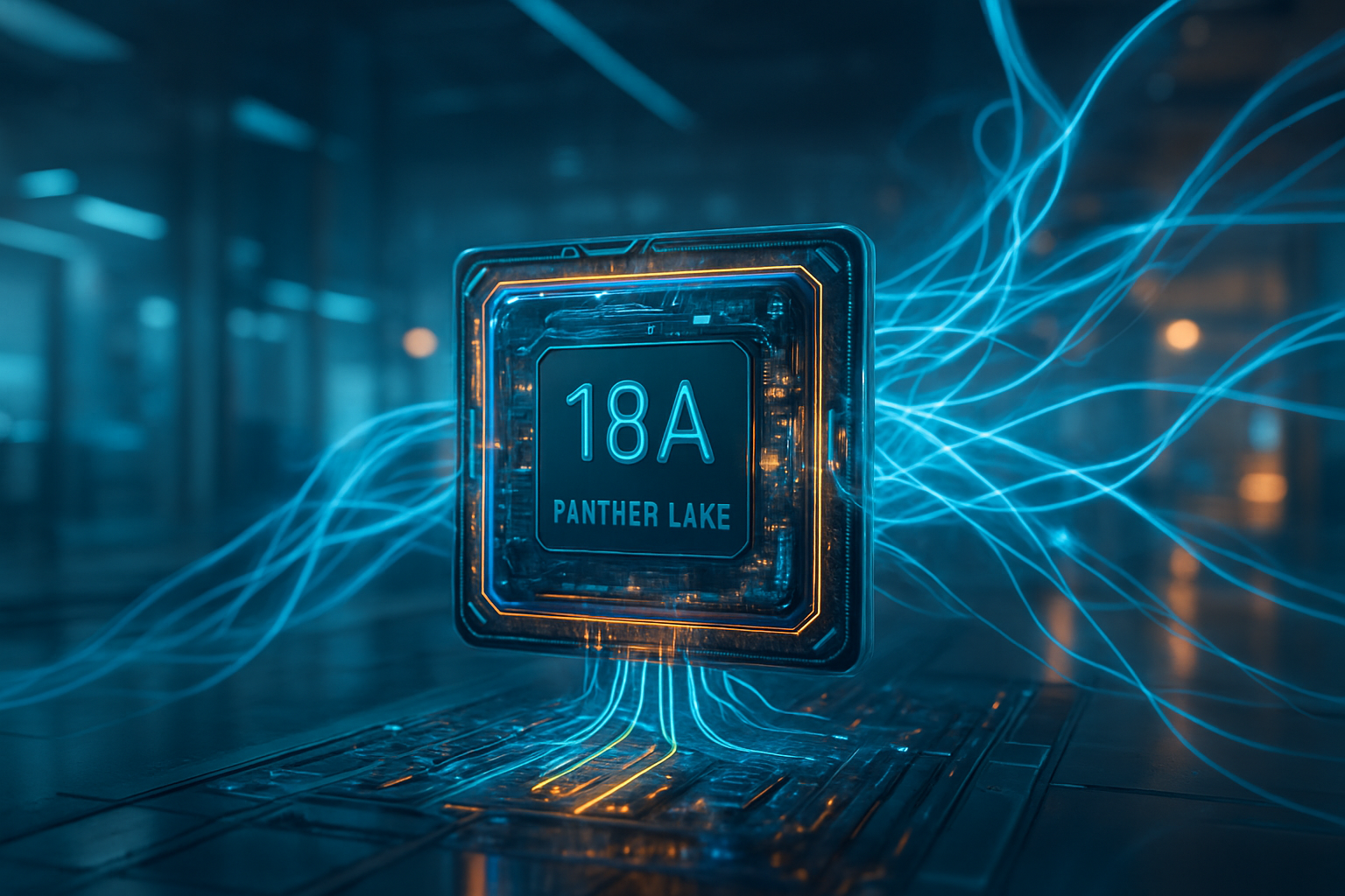
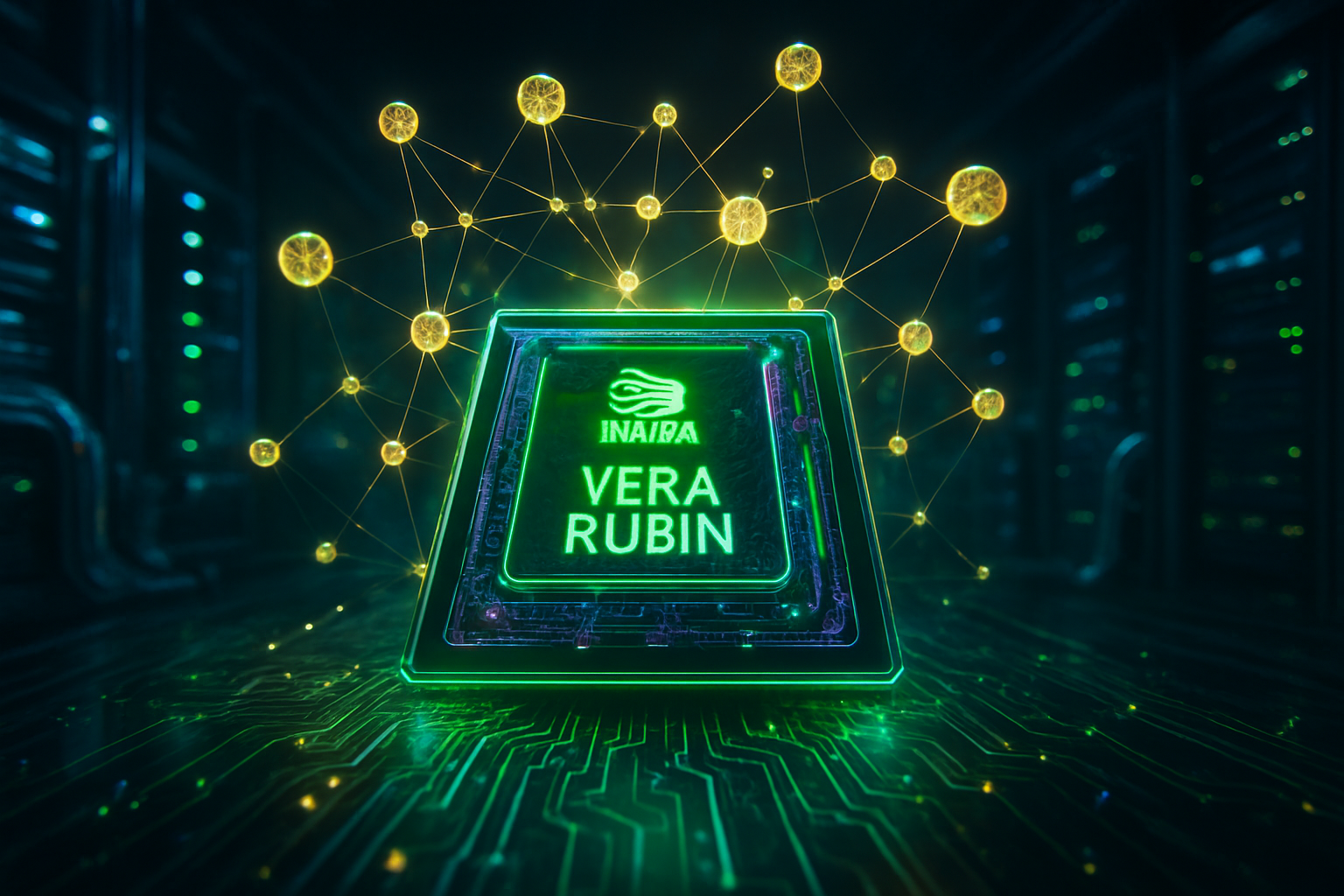
Tag: CES 2026

  • The 50+ TOPS Era Arrives at CES 2026: The AI PC Evolution Faces a Consumer Reality Check

    The 50+ TOPS Era Arrives at CES 2026: The AI PC Evolution Faces a Consumer Reality Check

    The halls of CES 2026 in Las Vegas have officially signaled the end of the "early adopter" phase for the AI PC, ushering in a new standard of local processing power that dwarfs the breakthroughs of just two years ago. For the first time, every major silicon provider—Intel (Intel Corp, NASDAQ: INTC), AMD (Advanced Micro Devices Inc, NASDAQ: AMD), and Qualcomm (Qualcomm Inc, NASDAQ: QCOM)—has demonstrated silicon capable of exceeding 50 Trillion Operations Per Second (TOPS) on the Neural Processing Unit (NPU) alone. This milestone marks the formal arrival of "Agentic AI," where PCs are no longer just running chatbots but are capable of managing autonomous background workflows without tethering to the cloud.

    However, as the hardware reaches these staggering new heights, a growing tension has emerged on the show floor. While the technical achievements of Intel's Core Ultra Series 3 and Qualcomm’s Snapdragon X2 Elite are undeniable, the industry is grappling with a widening "utility gap." Manufacturers are now facing a skeptical public that is increasingly confused by "AI Everywhere" branding and the abstract nature of NPU benchmarks, leading to a high-stakes debate over whether the "TOPS race" is driving genuine consumer demand or merely masking a plateau in traditional PC innovation.

    The Silicon Standard: 50 TOPS is the New Floor

    The technical center of gravity at CES 2026 was the official launch of the Intel Core Ultra Series 3, codenamed "Panther Lake." This architecture represents a historic pivot for Intel, being the first high-volume platform built on the ambitious Intel 18A (2nm-class) process. The Panther Lake NPU 5 architecture delivers a dedicated 50 TOPS, but the real story lies in the "Platform TOPS." By leveraging the integrated Arc Xe3 "Celestial" graphics, Intel claims total AI throughput of up to 170 TOPS, a leap intended to facilitate complex local image generation and real-time video manipulation that previously required a discrete GPU.

    Not to be outdone, Qualcomm dominated the high-end NPU category with its Snapdragon X2 Elite and Plus series. While Intel and AMD focused on balanced architectures, Qualcomm leaned into raw NPU efficiency, delivering a uniform 80 TOPS across its entire X2 stack. HP (HP Inc, NYSE: HPQ) even showcased a specialized OmniBook Ultra 14 featuring a "tuned" X2 variant that hits 85 TOPS. This silicon is built on the 3rd Gen Oryon CPU, utilizing a 3nm process that Qualcomm claims offers the best performance-per-watt for sustained AI workloads, such as local language model (LLM) fine-tuning.

    AMD rounded out the "Big Three" by unveiling the Ryzen AI 400 Series, codenamed "Gorgon Point." While AMD confirmed that its true next-generation "Medusa" (Zen 6) architecture won't hit mobile devices until 2027, the Gorgon Point refresh provides a bridge with an upgraded XDNA 2 NPU delivering 60 TOPS. The industry response has been one of technical awe but practical caution; researchers note that while we have more than doubled NPU performance since 2024’s Copilot+ launch, the software ecosystem is still struggling to utilize this much local "headroom" effectively.

    Industry Implications: The "Megahertz Race" 2.0

    This surge in NPU performance has forced Microsoft (Microsoft Corp, NASDAQ: MSFT) to evolve its Copilot+ PC requirements. While the official baseline remains at 40 TOPS, the 2026 hardware landscape has effectively treated 50 TOPS as the "new floor" for premium Windows 11 devices. Microsoft’s introduction of the "Windows AI Foundry" at the show further complicates the competitive landscape. This software layer allows Windows to dynamically offload AI tasks to the CPU, GPU, or NPU depending on thermal and battery constraints, potentially de-emphasizing the "NPU-only" marketing that Qualcomm and Intel have relied upon.

    The competitive stakes have never been higher for the silicon giants. For Intel, Panther Lake is a "must-win" moment to prove their 18A process can compete with TSMC's 2nm nodes. For Qualcomm, the X2 Elite is a bid to maintain its lead in the "Always Connected" PC space before Intel and AMD fully catch up in efficiency. However, the aggressive marketing of these specs has led to what analysts are calling the "Megahertz Race 2.0." Much like the clock-speed wars of the 1990s, the focus on TOPS is beginning to yield diminishing returns for the average user, creating an opening for Apple (Apple Inc, NASDAQ: AAPL) to continue its "it just works" narrative with Apple Intelligence, which focuses on integrated features rather than raw NPU metrics.

    The Branding Backlash: "AI Everywhere" vs. Consumer Reality

    Despite the technical triumphs, CES 2026 was marked by a notable "Honesty Offensive." In a surprising move, executives from Dell (Dell Technologies Inc, NYSE: DELL) admitted during a keynote panel that the broad "AI PC" branding has largely failed to ignite the massive upgrade cycle the industry anticipated in 2025. Consumers are reportedly suffering from "naming fatigue," finding it difficult to distinguish between "AI-Advanced," "Copilot+," and "AI-Ready" machines. The debate on the show floor centered on whether the NPU is a "killer feature" or simply a new commodity, much like the transition from integrated to high-definition audio decades ago.

    Furthermore, a technical consensus is emerging that raw TOPS may be the wrong metric for consumers to follow. Analysts at Gartner and IDC pointed out that local AI performance is increasingly "memory-bound" rather than "compute-bound." A laptop with a 100 TOPS NPU but only 16GB of RAM will struggle to run the 2026-era 7B-parameter models that power the most useful autonomous agents. With global memory shortages driving up DDR5 and HBM prices, the "true" AI PC is becoming prohibitively expensive, leading many consumers to stick with older hardware and rely on superior cloud-based models like GPT-5 or Claude 4.

    Future Outlook: The Search for the "Killer App"

    Looking toward the remainder of 2026, the industry is shifting its focus from hardware specs to the elusive "killer app." The next frontier is "Sovereign AI"—the ability for users to own their data and intelligence entirely offline. We expect to see a rise in "Personal AI Operating Systems" that use these 50+ TOPS NPUs to index every file, email, and meeting locally, providing a privacy-first alternative to cloud-integrated assistants. This could finally provide the clear utility that justifies the "AI PC" premium.

    The long-term challenge remains the transition to 2nm and 3nm manufacturing. While 2026 is the year of the 50 TOPS floor, 2027 is already being teased as the year of the "100 TOPS NPU" with AMD’s Medusa and Intel’s Nova Lake. However, unless software developers can find ways to make this power "invisible"—optimizing battery life and thermals silently rather than demanding user interaction—the hardware may continue to outpace the average consumer's needs.

    A Crucial Turning Point for Personal Computing

    CES 2026 will likely be remembered as the year the AI PC matured from a marketing experiment into a standardized hardware category. The arrival of 50+ TOPS silicon from Intel, AMD, and Qualcomm has fundamentally raised the ceiling for what a portable device can do, moving us closer to a world where our computers act as proactive partners rather than passive tools. Intel's Panther Lake and Qualcomm's X2 Elite represent the pinnacle of current engineering, proving that the technical hurdles of on-device AI are being cleared with remarkable speed.

    However, the industry's focus must now pivot from "more" to "better." The confusion surrounding AI branding and the skepticism toward raw TOPS benchmarks suggest that the "TOPS race" is reaching its limit as a sales driver. In the coming months, the success of the AI PC will depend less on the trillion operations per second it can perform and more on its ability to offer tangible, private, and indispensable utility. For now, the hardware is ready; the question is whether the software—and the consumer—is prepared to follow.


    This content is intended for informational purposes only and represents analysis of current AI developments.

    TokenRing AI delivers enterprise-grade solutions for multi-agent AI workflow orchestration, AI-powered development tools, and seamless remote collaboration platforms.
    For more information, visit https://www.tokenring.ai/.

  • The Silicon Revolution: Synopsys and NVIDIA Redefine the Future of Chip Design at CES 2026

    The Silicon Revolution: Synopsys and NVIDIA Redefine the Future of Chip Design at CES 2026

    The semiconductor industry reached a historic turning point at CES 2026 as Synopsys (NASDAQ: SNPS) and NVIDIA (NASDAQ: NVDA) unveiled a series of AI-driven breakthroughs that promise to fundamentally alter how the world's most complex chips are designed and manufactured. Central to the announcement was the maturation of the Synopsys.ai platform, which has transitioned from an experimental toolset into an industrial powerhouse capable of reducing chip design cycles by as much as 12 months. This acceleration represents a seismic shift for the technology sector, effectively compressing three years of traditional research and development into two.

    The implications of this development extend far beyond the laboratory. By leveraging "agentic" AI and high-fidelity virtual prototyping, Synopsys is enabling a "software-first" approach to engineering, particularly in the burgeoning field of software-defined vehicles (SDVs). As chips become more complex at the 2nm and sub-2nm nodes, the traditional bottlenecks of physical prototyping and manual verification are being replaced by AI-native workflows. This evolution is being fueled by a multi-billion dollar commitment from NVIDIA, which is increasingly treating Electronic Design Automation (EDA) not just as a tool, but as a core pillar of its own hardware dominance.

    AgentEngineer and the Rise of Autonomous Chip Design

    The technical centerpiece of Synopsys’ CES showcase was the introduction of AgentEngineer™, an agentic AI framework that marks the next evolution of the Synopsys.ai suite. Unlike previous AI tools that functioned as simple assistants, AgentEngineer utilizes autonomous AI agents capable of reasoning, planning, and executing complex engineering tasks with minimal human intervention. These agents can handle "high-toil" repetitive tasks such as design rule checking, layout optimization, and verification, allowing human engineers to focus on high-level architecture.

    Synopsys also debuted its expanded virtualization portfolio, which integrates technology from its strategic acquisition of Ansys. This integration allows for the creation of "digital twins" of entire electronic stacks long before physical silicon exists. At the heart of this are new Virtualizer Development Kits (VDKs) designed for next-generation automotive architectures, including the Arm Zena compute subsystems and high-performance cores from NXP Semiconductors (NASDAQ: NXPI) and Texas Instruments (NASDAQ: TXN). By providing software teams with virtual System-on-Chip (SoC) models months in advance, Synopsys claims that the time for full system bring-up—once a grueling multi-month process—can now be completed in just a few days.

    This approach differs radically from previous EDA methodologies, which relied heavily on "sequential" development—where software development waited for hardware prototypes. The new "shift-left" paradigm allows for parallel development, slashing the time-to-market for complex systems. Industry experts have noted that the integration of multiphysics simulation (heat, stress, and electromagnetics) directly into the AI design loop represents a breakthrough that was considered a "holy grail" only a few years ago.

    NVIDIA’s $2 Billion Bet on the EDA Ecosystem

    The industry's confidence in this AI-driven future was underscored by NVIDIA’s massive strategic investment. In a move that sent shockwaves through the market, NVIDIA has committed approximately $2 billion to expand its partnership with Synopsys, purchasing millions of shares and deepening technical integration. NVIDIA is no longer just a customer of EDA tools; it is co-architecting the infrastructure. By accelerating the Synopsys EDA stack with its own CUDA libraries and GPU clusters, NVIDIA is optimizing its upcoming GPU architectures—including the newly announced Rubin platform—using the very tools it is helping to build.

    This partnership places significant pressure on other major players in the EDA space, such as Cadence Design Systems (NASDAQ: CDNS) and Siemens (OTC: SIEGY). At CES 2026, NVIDIA also announced an "Industrial AI Operating System" in collaboration with Siemens, which aims to bring generative and agentic workflows to the factory floor and PCB design. The competitive landscape is shifting from who has the best algorithms to who has the most integrated AI-native design stack backed by massive GPU compute power.

    For tech giants and startups alike, this development creates a "winner-takes-most" dynamic. Companies that can afford to integrate these high-end, AI-driven EDA tools will be able to iterate on hardware at a pace that traditional competitors cannot match. Startups in the AI chip space, in particular, may find the 12-month reduction in design cycles to be their only path to survival in a market where hardware becomes obsolete in eighteen months.

    A New Era of "Computers on Wheels" and 2nm Complexity

    The wider significance of these advancements lies in their ability to solve the "complexity wall" of sub-2nm manufacturing. As transistors approach atomic scales, the physics of chip design becomes increasingly unpredictable. AI is the only tool capable of managing the quadrillions of design variables involved in modern lithography. NVIDIA’s cuLitho computational lithography library, integrated with Synopsys and TSMC (NYSE: TSM) workflows, has already reduced lithography simulation times from weeks to overnight, making the mass production of 2nm chips economically viable.

    This shift is most visible in the automotive sector. The "software-defined vehicle" is no longer a buzzword; it is a necessity as cars transition into data centers on wheels. By virtualizing the entire vehicle electronics stack, Synopsys and its partners are reducing prototyping and testing costs by 20% to 60%. This fits into a broader trend where AI is being used to bridge the gap between the digital and physical worlds, a trend seen in other sectors like robotics and aerospace.

    However, the move toward autonomous AI designers also raises concerns. Industry leaders have voiced caution regarding the "black box" nature of AI-generated designs and the potential for systemic errors that human engineers might overlook. Furthermore, the concentration of such powerful design tools in the hands of a few dominant players could lead to a bottleneck in global innovation if access is not democratized.

    The Horizon: From Vera CPUs to Fully Autonomous Fab Integration

    Looking forward, the next two years are expected to bring even deeper integration between AI reasoning and hardware manufacturing. Experts predict that NVIDIA’s Vera CPU—specifically designed for reasoning-heavy agentic AI—will become the primary engine for next-generation EDA workstations. These systems will likely move beyond "assisting" designers to proposing entire architectural configurations based on high-level performance goals, a concept known as "intent-based design."

    The long-term goal is a closed-loop system where AI-driven EDA tools are directly linked to semiconductor fabrication plants (fabs). In this scenario, the design software would receive real-time telemetry from the manufacturing line, automatically adjusting chip layouts to account for minute variations in the production process. While challenges remain—particularly in the standardization of data across different vendors—the progress shown at CES 2026 suggests these hurdles are being cleared faster than anticipated.

    Conclusion: The Acceleration of Human Ingenuity

    The announcements from Synopsys and NVIDIA at CES 2026 mark a definitive end to the era of manual chip design. The ability to slash a year off the development cycle of a modern SoC is a feat of engineering that will ripple through every corner of the global economy, from faster smartphones to safer autonomous vehicles. The integration of agentic AI and virtual prototyping has turned the "shift-left" philosophy from a theoretical goal into a practical reality.

    As we look toward the remainder of 2026, the industry will be watching closely to see how these tools perform in high-volume production environments. The true test will be the first wave of 2nm AI chips designed entirely within these new autonomous frameworks. For now, one thing is certain: the speed of innovation is no longer limited by how fast we can draw circuits, but by how fast we can train the AI to draw them for us.


    This content is intended for informational purposes only and represents analysis of current AI developments.

    TokenRing AI delivers enterprise-grade solutions for multi-agent AI workflow orchestration, AI-powered development tools, and seamless remote collaboration platforms.
    For more information, visit https://www.tokenring.ai/.

  • The 2,048-Bit Breakthrough: Inside the HBM4 Memory War at CES 2026

    The 2,048-Bit Breakthrough: Inside the HBM4 Memory War at CES 2026

    The Consumer Electronics Show (CES) 2026 has officially transitioned from a showcase of consumer gadgets to the primary battlefield for the most critical component in the artificial intelligence era: High Bandwidth Memory (HBM). What industry analysts are calling the "HBM4 Memory War" reached a fever pitch this week in Las Vegas, as the world’s leading semiconductor giants unveiled their most advanced memory architectures to date. The stakes have never been higher, as these chips represent the fundamental infrastructure required to power the next generation of generative AI models and autonomous systems.

    At the center of the storm is the formal introduction of the HBM4 standard, a revolutionary leap in memory technology designed to shatter the "memory wall" that has plagued AI scaling. As NVIDIA (NASDAQ: NVDA) prepares to launch its highly anticipated "Rubin" GPU architecture, the race to supply the necessary bandwidth has seen SK Hynix (KRX: 000660), Samsung Electronics (KRX: 005930), and Micron Technology (NASDAQ: MU) deploy their most aggressive technological roadmaps in history. The victor of this conflict will likely dictate the pace of AI development for the remainder of the decade.

    Engineering the 16-Layer Titan

    SK Hynix stole the spotlight at CES 2026 by demonstrating the world’s first 16-layer (16-Hi) HBM4 module, a massive 48GB stack that represents a nearly 50% increase in capacity over current HBM3E solutions. The technical centerpiece of this announcement is the implementation of a 2,048-bit interface—double the 1,024-bit width that has been the industry standard for a decade. By "widening the pipe" rather than simply increasing clock speeds, SK Hynix has achieved an unprecedented data throughput of 1.6 TB/s per stack, all while significantly reducing the power consumption and heat generation that have become major obstacles in modern data centers.

    To achieve this 16-layer density, SK Hynix utilized its proprietary Advanced Mass Reflow Molded Underfill (MR-MUF) technology, thinning individual DRAM wafers to a staggering 30 micrometers—roughly the thickness of a human hair. This allows the company to stack 16 layers of high-density DRAM within the same physical height as previous 12-layer designs. Furthermore, the company highlighted a strategic alliance with TSMC (NYSE: TSM), using a specialized 12nm logic base die at the bottom of the stack. This collaboration allows for deeper integration between the memory and the processor, effectively turning the memory stack into a semi-intelligent co-processor that can handle basic data pre-processing tasks.

    Initial reactions from the semiconductor research community have been overwhelmingly positive, though some experts caution about the manufacturing complexity. Dr. Elena Vos, Lead Architect at Silicon Analytics, noted that while the 2,048-bit interface is a "masterstroke of efficiency," the move toward hybrid bonding and extreme wafer thinning raises significant yield concerns. However, SK Hynix’s demonstration showed functional silicon running at 10 GT/s, suggesting that the company is much closer to mass production than its rivals might have hoped.

    A Three-Way Clash for AI Dominance

    While SK Hynix focused on density and interface width, Samsung Electronics counter-attacked with a focus on manufacturing efficiency and power. Samsung unveiled its HBM4 lineup based on its 1c nanometer process—the sixth generation of its 10nm-class DRAM. Samsung claims that this advanced node provides a 40% improvement in energy efficiency compared to competing 1b-based modules. In an era where NVIDIA's top-tier GPUs are pushing past 1,000 watts, Samsung is positioning its HBM4 as the only viable solution for sustainable, large-scale AI deployments. Samsung also signaled a massive production ramp-up at its Pyeongtaek facility, aiming to reach 250,000 wafers per month by the end of the year to meet the insatiable demand from hyperscalers.

    Micron Technology, meanwhile, is leveraging its status as a highly efficient "third player" to disrupt the market. Micron used CES 2026 to announce that its entire HBM4 production capacity for the year has already been sold out through advance contracts. With a $20 billion capital expenditure plan and new manufacturing sites in Taiwan and Japan, Micron is banking on a "supply-first" strategy. While their early HBM4 modules focus on 12-layer stacks, they have promised a rapid transition to "HBM4E" by 2027, featuring 64GB capacities. This aggressive roadmap is clearly aimed at winning a larger share of the bill of materials for NVIDIA’s upcoming Rubin platform.

    The primary beneficiary of this memory war is undoubtedly NVIDIA. The upcoming Rubin GPU is expected to utilize eight stacks of HBM4, providing a total of 384GB of high-speed memory and an aggregate bandwidth of 22 TB/s. This is nearly triple the bandwidth of the current Blackwell architecture, a requirement driven by the move toward "Reasoning Models" and Mixture-of-Experts (MoE) architectures that require massive amounts of data to be swapped in and out of the GPU memory at lightning speed.

    Shattering the Memory Wall: The Strategic Stakes

    The significance of the HBM4 transition extends far beyond simple speed increases; it represents a fundamental shift in how computers are built. For decades, the "Von Neumann bottleneck"—the delay caused by the distance and speed limits between a processor and its memory—has limited computational performance. HBM4, with its 2,048-bit interface and logic-die integration, essentially fuses the memory and the processor together. This is the first time in history where memory is not just a storage bin, but a customized, active participant in the AI computation process.

    This development is also a critical geopolitical and economic milestone. As nations race toward "Sovereign AI," the ability to secure a stable supply of high-performance memory has become a matter of national security. The massive capital requirements—running into the tens of billions of dollars for each company—ensure that the HBM market remains a highly exclusive club. This consolidation of power among SK Hynix, Samsung, and Micron creates a strategic choke point in the global AI supply chain, making these companies as influential as the foundries that print the AI chips themselves.

    However, the "war" also brings concerns regarding the environmental footprint of AI. While HBM4 is more efficient per gigabyte of data transferred, the sheer scale of the units being deployed will lead to a net increase in data center power consumption. The shift toward 1,000-watt GPUs and multi-kilowatt server racks is forcing a total rethink of liquid cooling and power delivery infrastructure, creating a secondary market boom for cooling specialists and electrical equipment manufacturers.

    The Horizon: Custom Logic and the Road to HBM5

    Looking ahead, the next phase of the memory war will likely involve "Custom HBM." At CES 2026, both SK Hynix and Samsung hinted at future products where customers like Google or Amazon (NASDAQ: AMZN) could provide their own proprietary logic to be integrated directly into the HBM4 base die. This would allow for even more specialized AI acceleration, potentially moving functions like encryption, compression, and data search directly into the memory stack itself.

    In the near term, the industry will be watching the "yield race" closely. Demonstrating a 16-layer stack at a trade show is one thing; consistently manufacturing them at the millions-per-month scale required by NVIDIA is another. Experts predict that the first half of 2026 will be defined by rigorous qualification tests, with the first Rubin-powered servers hitting the market late in the fourth quarter. Meanwhile, whisperings of HBM5 are already beginning, with early proposals suggesting another doubling of the interface or the move to 3D-integrated memory-on-logic architectures.

    A Decisive Moment for the AI Hardware Stack

    The CES 2026 HBM4 announcements represent a watershed moment in semiconductor history. We are witnessing the end of the "general purpose" memory era and the dawn of the "application-specific" memory age. SK Hynix’s 16-Hi breakthrough and Samsung’s 1c process efficiency are not just technical achievements; they are the enabling technologies that will determine whether AI can continue its exponential growth or if it will be throttled by hardware limitations.

    As we move forward into 2026, the key indicators of success will be yield rates and the ability of these manufacturers to manage the thermal complexities of 3D stacking. The "Memory War" is far from over, but the opening salvos at CES have made one thing clear: the future of artificial intelligence is no longer just about the speed of the processor—it is about the width and depth of the memory that feeds it. Investors and tech leaders should watch for the first Rubin-HBM4 benchmark results in early Q3 for the next major signal of where the industry is headed.


    This content is intended for informational purposes only and represents analysis of current AI developments.

    TokenRing AI delivers enterprise-grade solutions for multi-agent AI workflow orchestration, AI-powered development tools, and seamless remote collaboration platforms.
    For more information, visit https://www.tokenring.ai/.

  • Intel Reclaims the Silicon Crown: Panther Lake and the 18A Revolution Debut at CES 2026

    Intel Reclaims the Silicon Crown: Panther Lake and the 18A Revolution Debut at CES 2026

    The technological landscape shifted decisively at CES 2026 as Intel Corporation (NASDAQ: INTC) officially unveiled its "Panther Lake" processors, branded as the Core Ultra Series 3. This landmark release represents more than just a seasonal hardware update; it is the definitive debut of the Intel 18A (1.8nm) manufacturing process, a node that the company has bet its entire future on. For the first time in nearly a decade, Intel appears to have leaped ahead of its competitors in semiconductor density and power delivery, effectively signaling the end of the "efficiency gap" that has plagued x86 architecture since the rise of ARM-based alternatives.

    The immediate significance of the Core Ultra Series 3 lies in its unprecedented combination of raw compute power and mobile endurance. By achieving a staggering 27 hours of battery life on standard reference designs, Intel has effectively eliminated "battery anxiety" for the professional and creative classes. This launch is the culmination of Intel CEO Pat Gelsinger’s "five nodes in four years" strategy, moving the company from a period of manufacturing stagnation to the bleeding edge of the sub-2nm era.

    The Engineering Marvel of 18A: RibbonFET and PowerVia

    At the heart of Panther Lake is the Intel 18A process, which introduces two foundational shifts in transistor physics: RibbonFET and PowerVia. RibbonFET is Intel’s first implementation of Gate-All-Around (GAA) architecture, allowing for more precise control over the electrical current and significantly reducing power leakage compared to the aging FinFET designs. Complementing this is PowerVia, the industry’s first backside power delivery network. By moving power routing to the back of the wafer and keeping data signals on the front, Intel has reduced electrical resistance and simplified the manufacturing process, resulting in an estimated 20% gain in overall efficiency.

    The architectural layout of the Core Ultra Series 3 follows a sophisticated hybrid design. It features the new "Cougar Cove" Performance-cores (P-cores) and "Darkmont" Efficiency-cores (E-cores). While Cougar Cove provides a respectable 10% gain in instructions per clock (IPC) for single-threaded tasks, the true star is the multithreaded performance. Intel’s benchmarks show a 60% improvement in multithreaded workloads compared to the previous "Lunar Lake" generation, specifically when operating within a constrained 25W power envelope. This allows thin-and-light ultrabooks to tackle heavy video editing and compilation tasks that previously required bulky gaming laptops.

    Furthermore, the integrated graphics have undergone a radical transformation with the Xe3 "Celestial" architecture. The flagship SKUs, featuring the Arc B390 integrated GPU, boast a 77% leap in gaming performance over the previous generation. In early testing, this iGPU outperformed the dedicated mobile offerings from several mid-range competitors, enabling high-fidelity 1080p gaming on devices weighing less than three pounds. This is supplemented by the fifth-generation NPU (NPU 5), which delivers 50 TOPS of AI-specific compute, pushing the total platform AI performance to a massive 180 TOPS.

    Market Disruption and the Return of the Foundry King

    The debut of Panther Lake has sent shockwaves through the semiconductor market, directly challenging the recent gains made by Advanced Micro Devices (NASDAQ: AMD) and Qualcomm (NASDAQ: QCOM). While AMD’s "Gorgon Point" Ryzen AI 400 series remains a formidable opponent in the enthusiast space, Intel’s 18A process gives it a temporary but clear lead in the "performance-per-watt" metric that dominates the lucrative corporate laptop market. Qualcomm, which had briefly held the battery life crown with its Snapdragon X Elite series, now finds its efficiency advantage largely neutralized by the 27-hour runtime of the Core Ultra Series 3, all while Intel maintains a significant lead in native x86 software compatibility.

    The strategic implications extend beyond consumer chips. The successful high-volume rollout of 18A has revitalized Intel’s foundry business. Industry analysts at firms like KeyBanc have already issued upgrades for Intel stock, citing the Panther Lake launch as proof that Intel can once again compete with TSMC at the leading edge. Rumors of a $5 billion strategic investment from Nvidia (NASDAQ: NVDA) into Intel’s foundry capacity have intensified following the CES announcement, as the industry seeks to diversify manufacturing away from geopolitical flashpoints.

    Major OEMs including Dell, Lenovo, and MSI have responded with the most aggressive product refreshes in years. Dell’s updated XPS line and MSI’s Prestige series are both expected to ship with Panther Lake exclusively in their flagship configurations. This widespread adoption suggests that the "Intel Inside" brand has regained its prestige among hardware partners who had previously flirted with ARM-based designs or shifted focus to AMD.

    Agentic AI and the End of the Cloud Dependency

    The broader significance of Panther Lake lies in its role as a catalyst for "Agentic AI." By providing 180 total platform TOPS, Intel is enabling a shift from simple chatbots to autonomous AI agents that live and run entirely on the user's device. For the first time, thin-and-light laptops are capable of running 70-billion-parameter Large Language Models (LLMs) locally, ensuring data privacy and reducing latency for enterprise applications. This shift could fundamentally disrupt the business models of cloud-service providers, as companies move toward "on-device-first" AI policies.

    This release also marks a critical milestone in the global semiconductor race. As the first major platform built on 18A in the United States, Panther Lake is a flagship for the U.S. government’s goals of domestic manufacturing resilience. It represents a successful pivot from the "Intel 7" and "Intel 4" delays of the early 2020s, showing that the company has regained its footing in extreme ultraviolet (EUV) lithography and advanced packaging.

    However, the launch is not without concerns. The complexity of the 18A node and the sheer number of new architectural components—Cougar Cove, Darkmont, Xe3, and NPU 5—raise questions about initial yields and supply chain stability. While Intel has promised high-volume availability by the second quarter of 2026, any production hiccups could give competitors a window to reclaim the narrative.

    Looking Ahead: The Road to Intel 14A

    Looking toward the near future, the success of Panther Lake sets the stage for the "Intel 14A" node, which is already in early development. Experts predict that the lessons learned from the 18A rollout will accelerate Intel’s move into even smaller nanometer classes, potentially reaching 1.4nm as early as 2027. We expect to see the "Agentic AI" ecosystem blossom over the next 12 months, with software developers releasing specialized local models for coding, creative writing, and real-time translation that take full advantage of the NPU 5’s capabilities.

    The next challenge for Intel will be extending this 18A dominance into the desktop and server markets. While Panther Lake is primarily mobile-focused, the upcoming "Clearwater Forest" Xeon chips will use a similar manufacturing foundation to challenge the data center dominance of competitors. If Intel can replicate the efficiency gains seen at CES 2026 in the server rack, the competitive landscape of the entire tech industry could look drastically different by 2027.

    A New Era for Computing

    In summary, the debut of the Core Ultra Series 3 "Panther Lake" at CES 2026 is a watershed moment for the computing industry. Intel has delivered on its promise of a 60% multithreaded performance boost and 27 hours of battery life, effectively reclaiming its position as a technology leader. The successful deployment of the 18A node validates years of intensive R&D and billions of dollars in investment, proving that the x86 architecture still has significant room for innovation.

    As we move through 2026, the tech world will be watching closely to see if Intel can maintain this momentum. The immediate focus will be on the retail availability of these new laptops and the real-world performance of the Xe3 graphics architecture. For now, the narrative has shifted: Intel is no longer the legacy giant struggling to keep up—it is once again the company setting the pace for the rest of the industry.


    This content is intended for informational purposes only and represents analysis of current AI developments.

    TokenRing AI delivers enterprise-grade solutions for multi-agent AI workflow orchestration, AI-powered development tools, and seamless remote collaboration platforms.
    For more information, visit https://www.tokenring.ai/.

  • NVIDIA’s ‘ChatGPT Moment’: Jensen Huang Unveils Alpamayo and the Dawn of Physical AI at CES 2026

    NVIDIA’s ‘ChatGPT Moment’: Jensen Huang Unveils Alpamayo and the Dawn of Physical AI at CES 2026

    At the 2026 Consumer Electronics Show (CES) in Las Vegas, NVIDIA (NASDAQ: NVDA) officially declared the arrival of the "ChatGPT moment" for physical AI and robotics. CEO Jensen Huang, in a visionary keynote, signaled a monumental pivot from generative AI focused on digital content to "embodied AI" that can perceive, reason, and interact with the physical world. This announcement marks a transition where AI moves beyond the confines of a screen and into the gears of global industry, infrastructure, and transportation.

    The centerpiece of this declaration was the launch of the Alpamayo platform, a comprehensive autonomous driving and robotics framework designed to bridge the gap between digital intelligence and physical execution. By integrating large-scale Vision-Language-Action (VLA) models with high-fidelity simulation, NVIDIA aims to standardize the "brain" of future autonomous agents. This move is not merely an incremental update; it is a fundamental restructuring of how machines learn to navigate and manipulate their environments, promising to do for robotics what large language models did for natural language processing.

    The Technical Core: Alpamayo and the Cosmos Architecture

    The Alpamayo platform represents a significant departure from previous "pattern matching" approaches to robotics. At its heart is Alpamayo 1, a 10-billion parameter Vision-Language-Action (VLA) model that utilizes chain-of-thought reasoning. Unlike traditional systems that react to sensor data using fixed algorithms, Alpamayo can process complex "edge cases"—such as a chaotic construction site or a pedestrian making an unpredictable gesture—and provide a "reasoning trace" that explains its chosen trajectory. This transparency is a breakthrough in AI safety, allowing developers to understand why a robot made a specific decision in real-time.

    Supporting Alpamayo is the new NVIDIA Cosmos architecture, which Huang described as the "operating system for the physical world." Cosmos includes three specialized models: Cosmos Predict, which generates high-fidelity video of potential future world states to help robots plan actions; Cosmos Transfer, which converts 3D spatial inputs into photorealistic simulations; and Cosmos Reason 2, a multimodal reasoning model that acts as a "physics critic." Together, these models allow robots to perform internal simulations of physics before moving an arm or accelerating a vehicle, drastically reducing the risk of real-world errors.

    To power these massive models, NVIDIA showcased the Vera Rubin hardware architecture. The successor to the Blackwell line, Rubin is a co-designed six-chip system featuring the Vera CPU and Rubin GPU, delivering a staggering 50 petaflops of inference capability. For edge applications, NVIDIA released the Jetson T4000, which brings Blackwell-level compute to compact robotic forms, enabling humanoid robots like the Isaac GR00T N1.6 to perform complex, multi-step tasks with 4x the efficiency of previous generations.

    Strategic Realignment and Market Disruption

    The launch of Alpamayo and the broader Physical AI roadmap has immediate implications for the global tech landscape. NVIDIA (NASDAQ: NVDA) is no longer positioning itself solely as a chipmaker but as the foundational platform for the "Industrial AI" era. By making Alpamayo an open-source family of models and datasets—including 1,700 hours of multi-sensor data from 2,500 cities—NVIDIA is effectively commoditizing the software layer of autonomous driving, a direct challenge to the proprietary "walled garden" approach favored by companies like Tesla (NASDAQ: TSLA).

    The announcement of a deepened partnership with Siemens (OTC: SIEGY) to create an "Industrial AI Operating System" positions NVIDIA as a critical player in the $500 billion manufacturing sector. The Siemens Electronics Factory in Erlangen, Germany, is already being utilized as the blueprint for a fully AI-driven adaptive manufacturing site. In this ecosystem, "Agentic AI" replaces rigid automation; robots powered by NVIDIA's Nemotron-3 and NIM microservices can now handle everything from PCB design to complex supply chain logistics without manual reprogramming.

    Analysts from J.P. Morgan (NYSE: JPM) and Wedbush have reacted with bullish enthusiasm, suggesting that NVIDIA’s move into physical AI could unlock a 40% upside in market valuation. Other partners, including Mercedes-Benz (OTC: MBGYY), have already committed to the Alpamayo stack, with the 2026 CLA model slated to be the first consumer vehicle to feature the full reasoning-based autonomous system. By providing the tools for Caterpillar (NYSE: CAT) and Foxconn to build autonomous agents, NVIDIA is successfully diversifying its revenue streams far beyond the data center.

    A Broader Significance: The Shift to Agentic AI

    NVIDIA’s "ChatGPT moment" signifies a profound shift in the broader AI landscape. We are moving from "Chatty AI"—systems that assist with emails and code—to "Competent AI"—systems that build cars, manage warehouses, and drive through city streets. This evolution is defined by World Foundation Models (WFMs) that possess an inherent understanding of physical laws, a milestone that many researchers believe is the final hurdle before achieving Artificial General Intelligence (AGI).

    However, this leap into physical AI brings significant concerns. The ability for machines to "reason" and act autonomously in public spaces raises questions about liability, cybersecurity, and the displacement of labor in manufacturing and logistics. Unlike a hallucination in a chatbot, a "hallucination" in a 40-ton autonomous truck or a factory arm has life-and-death consequences. NVIDIA’s focus on "reasoning traces" and the Cosmos Reason 2 critic model is a direct attempt to address these safety concerns, yet the "long tail" of unpredictable real-world scenarios remains a daunting challenge.

    The comparison to the original ChatGPT launch is apt because of the "zero-to-one" shift in capability. Before ChatGPT, LLMs were curiosities; afterward, they were infrastructure. Similarly, before Alpamayo and Cosmos, robotics was largely a field of specialized, rigid machines. NVIDIA is betting that CES 2026 will be remembered as the point where robotics became a general-purpose, software-defined technology, accessible to any industry with the compute power to run it.

    The Roadmap Ahead: 2026 and Beyond

    NVIDIA’s roadmap for the Alpamayo platform is aggressive. Following the CES announcement, the company expects to begin full-stack autonomous vehicle testing on U.S. roads in the first quarter of 2026. By late 2026, the first production vehicles using the Alpamayo stack will hit the market. Looking further ahead, NVIDIA and its partners aim to launch dedicated Robotaxi services in 2027, with the ultimate goal of achieving "peer-to-peer" fully autonomous driving—where consumer vehicles can navigate any environment without human intervention—by 2028.

    In the manufacturing sector, the rollout of the Digital Twin Composer in mid-2026 will allow factory managers to run "what-if" scenarios in a simulated environment that is perfectly synced with the physical world. This will enable factories to adapt to supply chain shocks or design changes in minutes rather than months. The challenge remains the integration of these high-level AI models with legacy industrial hardware, a hurdle that the Siemens partnership is specifically designed to overcome.

    Conclusion: A Turning Point in Industrial History

    The announcements at CES 2026 mark a definitive end to the era of AI as a digital-only phenomenon. By providing the hardware (Rubin), the software (Alpamayo), and the simulation environment (Cosmos), NVIDIA has positioned itself as the architect of the physical AI revolution. The "ChatGPT moment" for robotics is not just a marketing slogan; it is a declaration that the physical world is now as programmable as the digital one.

    The long-term impact of this development cannot be overstated. As autonomous agents become ubiquitous in manufacturing, construction, and transportation, the global economy will likely experience a productivity surge unlike anything seen since the Industrial Revolution. For now, the tech world will be watching closely as the first Alpamayo-powered vehicles and "Agentic" factories go online in the coming months, testing whether NVIDIA's reasoning-based AI can truly master the unpredictable nature of reality.


    This content is intended for informational purposes only and represents analysis of current AI developments.

    TokenRing AI delivers enterprise-grade solutions for multi-agent AI workflow orchestration, AI-powered development tools, and seamless remote collaboration platforms.
    For more information, visit https://www.tokenring.ai/.

  • NVIDIA Unveils ‘Vera Rubin’ Architecture at CES 2026: The 10x Efficiency Leap Fueling the Next AI Industrial Revolution

    NVIDIA Unveils ‘Vera Rubin’ Architecture at CES 2026: The 10x Efficiency Leap Fueling the Next AI Industrial Revolution

    The 2026 Consumer Electronics Show (CES) kicked off with a seismic shift in the semiconductor landscape as NVIDIA (NASDAQ:NVDA) CEO Jensen Huang took the stage to unveil the "Vera Rubin" architecture. Named after the legendary astronomer who provided evidence for the existence of dark matter, the platform is designed to illuminate the next frontier of artificial intelligence: a world where inference is nearly free and AI "factories" drive a new industrial revolution. This announcement marks a critical turning point as the industry shifts from the "training era," characterized by massive compute clusters, to the "deployment era," where trillions of autonomous agents will require efficient, real-time reasoning.

    The centerpiece of the announcement was a staggering 10x reduction in inference costs compared to the previous Blackwell generation. By drastically lowering the barrier to entry for running sophisticated Mixture-of-Experts (MoE) models and large-scale reasoning agents, NVIDIA is positioning Vera Rubin not just as a hardware update, but as the foundational infrastructure for what Huang calls the "AI Industrial Revolution." With immediate backing from hyperscale partners like Microsoft (NASDAQ:MSFT) and specialized cloud providers like CoreWeave, the Vera Rubin platform is set to redefine the economics of intelligence.

    The Technical Backbone: R100 GPUs and the 'Olympus' Vera CPU

    The Vera Rubin architecture represents a departure from incremental gains, moving toward an "extreme codesign" philosophy that integrates six distinct chips into a unified supercomputer. At the heart of the system is the R100 GPU, manufactured on TSMC’s (NYSE:TSM) advanced 3nm (N3P) process. Boasting 336 billion transistors—a 1.6x density increase over Blackwell—the R100 is paired with the first-ever implementation of HBM4 memory. This allows for a massive 22 TB/s of memory bandwidth per chip, nearly tripling the throughput of previous generations and solving the "memory wall" that has long plagued high-performance computing.

    Complementing the GPU is the "Vera" CPU, featuring 88 custom-designed "Olympus" cores. These cores utilize "spatial multi-threading" to handle 176 simultaneous threads, delivering a 2x performance leap over the Grace CPU. The platform also introduces NVLink 6, an interconnect capable of 3.6 TB/s of bi-directional bandwidth, which enables the Vera Rubin NVL72 rack to function as a single, massive logical GPU. Perhaps the most innovative technical addition is the Inference Context Memory Storage (ICMS), powered by the new BlueField-4 DPU. This creates a dedicated storage tier for "KV cache," allowing AI agents to maintain long-term memory and reason across massive contexts without being throttled by on-chip GPU memory limits.

    Strategic Impact: Fortifying the AI Ecosystem

    The arrival of Vera Rubin cements NVIDIA’s dominance in the AI hardware market while deepening its ties with major cloud infrastructure players. Microsoft (NASDAQ:MSFT) Azure has already committed to being one of the first to deploy Vera Rubin systems within its upcoming "Fairwater" AI superfactories located in Wisconsin and Atlanta. These sites are being custom-engineered to handle the extreme power density and 100% liquid-cooling requirements of the NVL72 racks. For Microsoft, this provides a strategic advantage in hosting the next generation of OpenAI’s models, which are expected to rely heavily on the Rubin architecture's increased FP4 compute power.

    Specialized cloud provider CoreWeave is also positioned as a "first-mover" partner, with plans to integrate Rubin systems into its fleet by the second half of 2026. This move allows CoreWeave to maintain its edge as a high-performance alternative to traditional hyperscalers, offering developers direct access to the most efficient inference hardware available. The 10x reduction in token costs poses a significant challenge to competitors like AMD (NASDAQ:AMD) and Intel (NASDAQ:INTC), who must now race to match NVIDIA’s efficiency gains or risk being relegated to niche or budget-oriented segments of the market.

    Wider Significance: The Shift to Physical AI and Agentic Reasoning

    The theme of the "AI Industrial Revolution" signals a broader shift in how technology interacts with the physical world. NVIDIA is moving beyond chatbots and image generators toward "Physical AI"—autonomous systems that can perceive, reason, and act within industrial environments. Through an expanded partnership with Siemens (XETRA:SIE), NVIDIA is integrating the Rubin ecosystem into an "Industrial AI Operating System," allowing digital twins and robotics to automate complex workflows in manufacturing and energy sectors.

    This development also addresses the burgeoning "energy crisis" associated with AI scaling. By achieving a 5x improvement in power efficiency per token, the Vera Rubin architecture offers a path toward sustainable growth for data centers. It challenges the existing scaling laws, suggesting that intelligence can be "manufactured" more efficiently by optimizing inference rather than just throwing more raw power at training. This marks a shift from the era of "brute force" scaling to one of "intelligent efficiency," where the focus is on the quality of reasoning and the cost of deployment.

    Future Outlook: The Road to 2027 and Beyond

    Looking ahead, the Vera Rubin platform is expected to undergo an "Ultra" refresh in early 2027, potentially featuring up to 512GB of HBM4 memory. This will further enable the deployment of "World Models"—AI that can simulate physical reality with high fidelity for use in autonomous driving and scientific discovery. Experts predict that the next major challenge will be the networking infrastructure required to connect these "AI Factories" across global regions, an area where NVIDIA’s Spectrum-X Ethernet Photonics will play a crucial role.

    The focus will also shift toward "Sovereign AI," where nations build their own domestic Rubin-powered superclusters to ensure data privacy and technological independence. As the hardware becomes more efficient, the primary bottleneck may move from compute power to high-quality data and the refinement of agentic reasoning algorithms. We can expect to see a surge in startups focused on "Agentic Orchestration," building software layers that sit on top of Rubin’s ICMS to manage thousands of autonomous AI workers.

    Conclusion: A Milestone in Computing History

    The unveiling of the Vera Rubin architecture at CES 2026 represents more than just a new generation of chips; it is the infrastructure for a new era of global productivity. By delivering a 10x reduction in inference costs, NVIDIA has effectively democratized advanced AI reasoning, making it feasible for every business to integrate autonomous agents into their daily operations. The transition to a yearly product release cadence signals that the pace of AI innovation is not slowing down, but rather entering a state of perpetual acceleration.

    As we look toward the coming months, the focus will be on the successful deployment of the first Rubin-powered "AI Factories" by Microsoft and CoreWeave. The success of these sites will serve as the blueprint for the next decade of industrial growth. For the tech industry and society at large, the "Vera Rubin" era promises to be one where AI is no longer a novelty or a tool, but the very engine that powers the modern world.


    This content is intended for informational purposes only and represents analysis of current AI developments.

    TokenRing AI delivers enterprise-grade solutions for multi-agent AI workflow orchestration, AI-powered development tools, and seamless remote collaboration platforms.
    For more information, visit https://www.tokenring.ai/.

  • The Yotta-Scale War: AMD’s Helios Challenges NVIDIA’s Rubin for the Agentic AI Throne at CES 2026

    The Yotta-Scale War: AMD’s Helios Challenges NVIDIA’s Rubin for the Agentic AI Throne at CES 2026

    The landscape of artificial intelligence reached a historic inflection point at CES 2026, as the industry transitioned from the era of discrete GPUs to the era of unified, rack-scale "AI factories." The highlight of the event was the unveiling of the AMD (NASDAQ: AMD) Helios platform, a liquid-cooled, double-wide rack-scale architecture designed to push the boundaries of "yotta-scale" computing. This announcement sets the stage for a direct confrontation with NVIDIA (NASDAQ: NVDA) and its newly minted Vera Rubin platform, marking the most aggressive challenge to NVIDIA’s data center dominance in over a decade.

    The immediate significance of the Helios launch lies in its focus on "Agentic AI"—autonomous systems capable of long-running reasoning and multi-step task execution. By prioritizing massive High-Bandwidth Memory (HBM4) co-packaging and open-standard networking, AMD is positioning Helios not just as a hardware alternative, but as a fundamental shift toward an open ecosystem for the next generation of trillion-parameter models. As hyperscalers like OpenAI and Meta seek to diversify their infrastructure, the arrival of Helios signals the end of the single-vendor era and the birth of a true silicon duopoly in the high-end AI market.

    Technical Superiority and the Memory Wall

    The AMD Helios platform is a technical marvel that redefines the concept of a data center node. Each Helios rack is a liquid-cooled powerhouse containing 18 compute trays, with each tray housing four Instinct MI455X GPUs and one EPYC "Venice" CPU. This configuration yields a staggering 72 GPUs and 18 CPUs per rack, capable of delivering 2.9 ExaFLOPS of FP4 AI compute. The most striking specification is the integration of 31TB of HBM4 memory across the rack, with an aggregate bandwidth of 1.4PB/s. This "memory-first" approach is specifically designed to overcome the "memory wall" that has traditionally bottlenecked large-scale inference.

    In contrast, NVIDIA’s Vera Rubin platform focuses on "extreme co-design." The Rubin GPU features 288GB of HBM4 and is paired with the Vera CPU—an 88-core Armv9.2 chip featuring custom "Olympus" cores. While NVIDIA’s NVL72 rack delivers a slightly higher 3.6 ExaFLOPS of NVFP4 compute, its true innovation is the Inference Context Memory Storage (ICMS). Powered by the BlueField-4 DPU, ICMS acts as a shared, pod-level memory tier for Key-Value (KV) caches. This allows a fleet of AI agents to share a unified "context namespace," meaning that if one agent learns a piece of information, the entire pod can access it without redundant computation.

    The technical divergence between the two giants is clear: AMD is betting on raw, on-package memory density (432GB per GPU) to keep trillion-parameter models resident in high-speed memory, while NVIDIA is leveraging its vertical stack to create a sophisticated, software-defined memory hierarchy. Industry experts note that AMD’s reliance on the new Ultra Accelerator Link (UALink) for scale-up and Ultra Ethernet for scale-out networking represents a major victory for open standards, potentially lowering the barrier to entry for third-party hardware integration.

    Initial reactions from the AI research community have been overwhelmingly positive, particularly regarding the performance-per-watt gains. Both platforms utilize advanced 3D chiplet co-packaging and hybrid bonding, which significantly reduces the energy required to move data between logic and memory. This efficiency is crucial as the industry moves toward "yotta-scale" goals—computing at the scale of 10²⁴ operations per second—where power consumption becomes the primary limiting factor for data center expansion.

    Market Disruptions and the Silicon Duopoly

    The arrival of Helios and Rubin has profound implications for the competitive dynamics of the tech industry. For AMD (NASDAQ: AMD), Helios represents a "Milan moment"—a breakthrough that could see its data center market share jump from the low teens to nearly 20% by the end of 2026. The platform has already secured a massive endorsement from OpenAI, which announced a partnership for 6 gigawatts of AMD infrastructure. Perhaps more significantly, reports suggest AMD has issued warrants that could allow OpenAI to acquire up to a 10% stake in the company, a move that would cement a deep, structural alliance against NVIDIA’s dominance.

    NVIDIA (NASDAQ: NVDA), meanwhile, remains the incumbent titan, controlling approximately 80-85% of the AI accelerator market. Its transition to a one-year product cadence—moving from Blackwell to Rubin in record time—is a strategic maneuver designed to exhaust competitors. However, the "NVIDIA tax"—the high premium for its proprietary CUDA and NVLink stack—is driving hyperscalers like Alphabet (NASDAQ: GOOGL) and Microsoft (NASDAQ: MSFT) to aggressively fund "second source" options. By offering an open-standard alternative that matches or exceeds NVIDIA’s memory capacity, AMD is providing these giants with the leverage they have long sought.

    Startups and mid-tier AI labs stand to benefit from this competition through a projected 10x reduction in token generation costs. As AMD and NVIDIA battle for the "price-per-token" crown, the economic viability of complex, agentic AI workflows will improve. This could lead to a surge in new AI-native products that were previously too expensive to run at scale. Furthermore, the shift toward liquid-cooled, rack-scale systems will favor data center providers like Equinix (NASDAQ: EQIX) and Digital Realty (NYSE: DLR), who are already retrofitting facilities to handle the massive power and cooling requirements of these new "AI factories."

    The strategic advantage of the Helios platform also lies in its interoperability. By adhering to the Open Compute Project (OCP) standards, AMD is appealing to companies like Meta (NASDAQ: META), which has co-designed the Helios Open Rack Wide specification. This allows Meta to mix and match AMD hardware with its own in-house MTIA (Meta Training and Inference Accelerator) chips, creating a flexible, heterogeneous compute environment that reduces reliance on any single vendor's proprietary roadmap.

    The Dawn of Agentic AI and Yotta-Scale Infrastructure

    The competition between Helios and Rubin is more than a corporate rivalry; it is a reflection of the broader shift in the AI landscape toward "Agentic AI." Unlike the chatbots of 2023 and 2024, which responded to individual prompts, the agents of 2026 are designed to operate autonomously for hours or days, performing complex research, coding, and decision-making tasks. This shift requires a fundamentally different hardware architecture—one that can maintain massive "session histories" and provide low-latency access to vast amounts of context.

    AMD’s decision to pack 432GB of HBM4 onto a single GPU is a direct response to this need. It allows the largest models to stay "awake" and responsive without the latency penalties of moving data across a network. On the other hand, NVIDIA’s ICMS approach acknowledges that as agents become more complex, the cost of HBM will eventually become prohibitive, necessitating a tiered storage approach. These two different philosophies will likely coexist, with AMD winning in high-density inference and NVIDIA maintaining its lead in large-scale training and "Physical AI" (robotics and simulation).

    However, this rapid advancement brings potential concerns, particularly regarding the environmental impact and the concentration of power. The move toward yotta-scale computing requires unprecedented amounts of electricity, leading to a "power grab" where tech giants are increasingly investing in nuclear and renewable energy projects to sustain their AI ambitions. There is also the risk that the sheer cost of these rack-scale systems—estimated at $3 million to $5 million per rack—will further widen the gap between the "compute-rich" hyperscalers and the "compute-poor" academic and smaller research institutions.

    Comparatively, the leap from the H100 (Hopper) era to the Rubin/Helios era is significantly larger than the transition from V100 to A100. We are no longer just seeing faster chips; we are seeing the integration of memory, logic, and networking into a single, cohesive organism. This milestone mirrors the transition from mainframe computers to distributed clusters, but at an accelerated pace that is straining global supply chains, particularly for TSMC's 2nm and 3nm wafer capacity.

    Future Outlook: The Road to 2027

    Looking ahead, the next 18 to 24 months will be defined by the execution of these ambitious roadmaps. While both AMD and NVIDIA have unveiled their visions, the challenge now lies in mass production. NVIDIA’s Rubin is expected to enter production in late 2026, with shipping starting in Q4, while AMD’s Helios is slated for a Q3 2026 launch. The availability of HBM4 will be the primary bottleneck, as manufacturers like SK Hynix and Samsung (OTC: SSNLF) struggle to keep up with the demand for the complex 3D-stacked memory.

    In the near term, expect to see a surge in "Agentic AI" applications that leverage these new hardware capabilities. We will likely see the first truly autonomous enterprise departments—AI agents capable of managing entire supply chains or software development lifecycles with minimal human oversight. In the long term, the success of the Helios platform will depend on the maturity of AMD’s ROCm software ecosystem. While ROCm 7.2 has narrowed the gap with CUDA, providing "day-zero" support for major frameworks like PyTorch and vLLM, NVIDIA’s deep software moat remains a formidable barrier.

    Experts predict that the next frontier after yotta-scale will be "Neuromorphic-Hybrid" architectures, where traditional silicon is paired with specialized chips that mimic the human brain's efficiency. Until then, the battle will be fought in the data center trenches, with AMD and NVIDIA pushing the limits of physics to power the next generation of intelligence. The "Silicon Duopoly" is now a reality, and the beneficiaries will be the developers and enterprises that can harness this unprecedented scale of compute.

    Final Thoughts: A New Chapter in AI History

    The announcements at CES 2026 have made one thing clear: the era of the individual GPU is over. The competition for the data center crown has moved to the rack level, where the integration of compute, memory, and networking determines the winner. AMD’s Helios platform, with its massive HBM4 capacity and commitment to open standards, has proven that it is no longer just a "second source" but a primary architect of the AI future. NVIDIA’s Rubin, with its extreme co-design and innovative context management, continues to set the gold standard for performance and efficiency.

    As we look back on this development, it will likely be viewed as the moment when AI infrastructure finally caught up to the ambitions of AI researchers. The move toward yotta-scale computing and the support for agentic workflows will catalyze a new wave of innovation, transforming every sector of the global economy. For investors and industry watchers, the key will be to monitor the deployment speeds of these platforms and the adoption rates of the UALink and Ultra Ethernet standards.

    In the coming weeks, all eyes will be on the quarterly earnings calls of AMD (NASDAQ: AMD) and NVIDIA (NASDAQ: NVDA) for further details on supply chain allocations and early customer commitments. The "Yotta-Scale War" has only just begun, and its outcome will shape the trajectory of artificial intelligence for the rest of the decade.


    This content is intended for informational purposes only and represents analysis of current AI developments.

    TokenRing AI delivers enterprise-grade solutions for multi-agent AI workflow orchestration, AI-powered development tools, and seamless remote collaboration platforms.
    For more information, visit https://www.tokenring.ai/.

  • The HBM4 Memory War: SK Hynix, Samsung, and Micron Battle for AI Supremacy at CES 2026

    The HBM4 Memory War: SK Hynix, Samsung, and Micron Battle for AI Supremacy at CES 2026

    The floor of CES 2026 has transformed into a high-stakes battlefield for the semiconductor industry, as the "HBM4 Memory War" officially ignited among the world’s three largest memory manufacturers. With the artificial intelligence revolution entering a new phase of massive-scale model training, the demand for High Bandwidth Memory (HBM) has shifted from a supply-chain bottleneck to the primary architectural hurdle for next-generation silicon. The announcements made this week by SK Hynix, Samsung, and Micron represent more than just incremental speed bumps; they signal a fundamental shift in how memory and logic are integrated to power the most advanced AI clusters on the planet.

    This surge in memory innovation is being driven by the arrival of NVIDIA’s (NASDAQ:NVDA) new "Vera Rubin" architecture, the much-anticipated successor to the Blackwell platform. As AI models grow to tens of trillions of parameters, the industry has hit the "memory wall"—a physical limit where processors are fast enough to compute data, but the memory cannot feed it to them quickly enough. HBM4 is the industry's collective answer to this crisis, offering the massive bandwidth and energy efficiency required to prevent the world’s most expensive GPUs from sitting idle while waiting for data.

    The 16-Layer Breakthrough and the 1c Efficiency Edge

    At the center of the CES hardware showcase, SK Hynix (KRX:000660) stunned the industry by debuting the world’s first 16-layer (16-Hi) 48GB HBM4 stack. This engineering marvel doubles the density of previous generations while maintaining a strict 775µm height limit required by standard packaging. To achieve this, SK Hynix thinned individual DRAM wafers to just 30 micrometers—roughly one-third the thickness of a human hair—using its proprietary Advanced Mass Reflow Molded Underfill (MR-MUF) technology. The result is a single memory cube capable of an industry-leading 11.7 Gbps per pin, providing the sheer density needed for the ultra-large language models expected in late 2026.

    Samsung Electronics (KRX:005930) took a different strategic path, emphasizing its "one-stop shop" capability and manufacturing efficiency. Samsung’s HBM4 is built on its cutting-edge 1c (6th generation 10nm-class) DRAM process, which the company claims offers a 40% improvement in energy efficiency over current 1b-based modules. Unlike its competitors, Samsung is leveraging its internal foundry to produce both the memory and the logic base die, aiming to provide a more integrated and cost-effective solution. This vertical integration is a direct challenge to the partnership-driven models of its rivals, positioning Samsung as a turnkey provider for the HBM4 era.

    Not to be outdone, Micron Technology (NASDAQ:MU) announced an aggressive $20 billion capital expenditure plan for the coming fiscal year to fuel its capacity expansion. Micron’s HBM4 entry focuses on a 12-layer 36GB stack that utilizes a 2,048-bit interface—double the width of the HBM3E standard. By widening the data "pipe," Micron is achieving speeds exceeding 2.0 TB/s per stack. The company is rapidly scaling its "megaplants" in Taiwan and Japan, aiming to capture a significantly larger slice of the HBM market share, which SK Hynix has dominated for the past two years.

    Fueling the Rubin Revolution and Redefining Market Power

    The immediate beneficiary of this memory arms race is NVIDIA, whose Vera Rubin GPUs are designed to utilize eight stacks of HBM4 memory. With SK Hynix’s 48GB stacks, a single Rubin GPU could boast a staggering 384GB of high-speed memory, delivering an aggregate bandwidth of 22 TB/s. This is a nearly 3x increase over the Blackwell architecture, allowing for real-time inference of models that previously required entire server racks. The competitive implications are clear: the memory maker that can provide the highest yield of 16-layer stacks will likely secure the lion's share of NVIDIA's multi-billion dollar orders.

    For the broader tech landscape, this development creates a new hierarchy. Companies like Advanced Micro Devices (NASDAQ:AMD) are also pivoting their Instinct accelerator roadmaps to support HBM4, ensuring that the "memory war" isn't just an NVIDIA-exclusive event. However, the shift to HBM4 also elevates the importance of Taiwan Semiconductor Manufacturing Company (NYSE:TSM), which is collaborating with SK Hynix and Micron to manufacture the logic base dies that sit at the bottom of the HBM stack. This "foundry-memory" alliance is a direct competitive response to Samsung's internal vertical integration, creating two distinct camps in the semiconductor world: the specialists versus the integrated giants.

    Breaking the Memory Wall and the Shift to Logic-Integrated Memory

    The wider significance of HBM4 lies in its departure from traditional memory design. For the first time, the base die of the memory stack—the foundation upon which the DRAM layers sit—is being manufactured using advanced logic nodes (such as 5nm or 4nm). This effectively turns the memory stack into a "co-processor." By moving some of the data pre-processing and memory management directly into the HBM4 stack, engineers can reduce the energy-intensive data movement between the GPU and the memory, which currently accounts for a significant portion of a data center’s power consumption.

    This evolution is the most significant step yet in overcoming the "Memory Wall." In previous generations, the gap between compute speed and memory bandwidth was widening at an exponential rate. HBM4’s 2,048-bit interface and logic-integrated base die finally provide a roadmap to close that gap. This is not just a hardware upgrade; it is a fundamental rethinking of computer architecture that moves us closer to "near-memory computing," where the lines between where data is stored and where it is processed begin to blur.

    The Horizon: Custom HBM and the Path to HBM5

    Looking ahead, the next phase of this war will be fought on the ground of "Custom HBM" (cHBM). Experts at CES 2026 predict that by 2027, major AI players like Google or Amazon may begin commissioning HBM stacks with logic dies specifically designed for their own proprietary AI chips. This level of customization would allow for even greater efficiency gains, potentially tailoring the memory's internal logic to the specific mathematical operations required by a company's unique neural network architecture.

    The challenges remaining are largely thermal and yield-related. Stacking 16 layers of DRAM creates immense heat density, and the precision required to align thousands of Through-Silicon Vias (TSVs) across 16 layers is unprecedented. If yields on these 16-layer stacks remain low, the industry may see a prolonged period of supply shortages, keeping the price of AI compute high despite the massive capacity expansions currently underway at Micron and Samsung.

    A New Chapter in AI History

    The HBM4 announcements at CES 2026 mark a definitive turning point in the AI era. We have moved past the phase where raw FLOPs (Floating Point Operations per Second) were the only metric that mattered. Today, the ability to store, move, and access data at the speed of thought is the true measure of AI performance. The "Memory War" between SK Hynix, Samsung, and Micron is a testament to the critical role that specialized hardware plays in the advancement of artificial intelligence.

    In the coming weeks, the industry will be watching for the first third-party benchmarks of the Rubin architecture and the initial yield reports from the new HBM4 production lines. As these components begin to ship to data centers later this year, the impact will be felt in everything from the speed of scientific research to the capabilities of consumer-facing AI agents. The HBM4 era has arrived, and it is the high-octane fuel that will power the next decade of AI innovation.


    This content is intended for informational purposes only and represents analysis of current AI developments.

    TokenRing AI delivers enterprise-grade solutions for multi-agent AI workflow orchestration, AI-powered development tools, and seamless remote collaboration platforms.
    For more information, visit https://www.tokenring.ai/.

  • NVIDIA Unveils Vera Rubin Platform at CES 2026: A 10x Leap Toward the Era of Agentic AI

    NVIDIA Unveils Vera Rubin Platform at CES 2026: A 10x Leap Toward the Era of Agentic AI

    LAS VEGAS — In a landmark presentation at CES 2026, NVIDIA (NASDAQ: NVDA) has officially ushered in the next epoch of computing with the launch of the Vera Rubin platform. Named after the legendary astronomer who provided the first evidence of dark matter, the platform represents a total architectural overhaul designed to solve the most pressing bottleneck in modern technology: the transition from passive generative AI to autonomous, reasoning "agentic" AI.

    The announcement, delivered by CEO Jensen Huang to a capacity crowd, centers on a suite of six new chips that function as a singular, cohesive AI supercomputer. By integrating compute, networking, and memory at an unprecedented scale, NVIDIA claims the Vera Rubin platform will reduce AI inference costs by a factor of 10, effectively commoditizing high-level reasoning for enterprises and consumers alike.

    The Six Pillars of Rubin: A Masterclass in Extreme Codesign

    The Vera Rubin platform is built upon six foundational silicon advancements that NVIDIA describes as "extreme codesign." At the heart of the system is the Rubin GPU, a behemoth featuring 336 billion transistors and 288 GB of HBM4 memory. Delivering a staggering 22 TB/s of memory bandwidth per socket, the Rubin GPU is engineered to handle the massive Mixture-of-Experts (MoE) models that define the current state-of-the-art. Complementing the GPU is the Vera CPU, which marks a departure from traditional general-purpose processing. Featuring 88 custom "Olympus" cores compatible with Arm (NASDAQ: ARM) v9.2 architecture, the Vera CPU acts as a dedicated "data movement engine" optimized for the iterative logic and multi-step reasoning required by AI agents.

    The interconnect and networking stack has seen an equally dramatic upgrade. NVLink 6 doubles scale-up bandwidth to 3.6 TB/s per GPU, allowing a rack of 72 GPUs to act as a single, massive processor. On the scale-out side, the ConnectX-9 SuperNIC and Spectrum-6 Ethernet switch provide 1.6 Tb/s and 102.4 Tb/s of throughput, respectively, with the latter utilizing Co-Packaged Optics (CPO) for a 5x improvement in power efficiency. Finally, the BlueField-4 DPU introduces a dedicated Inference Context Memory Storage Platform, offloading Key-Value (KV) cache management to improve token throughput by 5x, effectively giving AI models a "long-term memory" during complex tasks.

    Microsoft and the Rise of the Fairwater AI Superfactories

    The immediate commercial impact of the Vera Rubin platform is being realized through a massive strategic partnership with Microsoft Corp. (NASDAQ: MSFT). Microsoft has been named the premier launch partner, integrating the Rubin architecture into its new "Fairwater" AI superfactories. These facilities, located in strategic hubs like Wisconsin and Atlanta, are designed to house hundreds of thousands of Vera Rubin Superchips in a unique three-dimensional rack configuration that minimizes cable runs and maximizes the efficiency of the NVLink 6 fabric.

    This partnership is a direct challenge to the broader cloud infrastructure market. By achieving a 10x reduction in inference costs, Microsoft and NVIDIA are positioning themselves to dominate the "agentic" era, where AI is not just a chatbot but a persistent digital employee performing complex workflows. For startups and competing AI labs, the Rubin platform raises the barrier to entry; training a 10-trillion parameter model now takes 75% fewer GPUs than it did on the previous Blackwell architecture. This shift effectively forces competitors to either adopt NVIDIA’s proprietary stack or face a massive disadvantage in both speed-to-market and operational cost.

    From Chatbots to Agents: The Reasoning Era

    The broader significance of the Vera Rubin platform lies in its explicit focus on "Agentic AI." While the previous generation of hardware was optimized for the "training era"—ingesting vast amounts of data to predict the next token—Rubin is built for the "reasoning era." This involves agents that can plan, use tools, and maintain context over weeks or months of interaction. The hardware-accelerated adaptive compression and the BlueField-4’s context management are specifically designed to handle the "long-context" requirements of these agents, allowing them to remember previous interactions and complex project requirements without the massive latency penalties of earlier systems.

    This development mirrors the historical shift from mainframe computing to the PC, or from the desktop to mobile. By making high-level reasoning 10 times cheaper, NVIDIA is enabling a world where every software application can have a dedicated, autonomous agent. However, this leap also brings concerns regarding the energy consumption of such massive clusters and the potential for rapid job displacement as AI agents become capable of handling increasingly complex white-collar tasks. Industry experts note that the Rubin platform is not just a faster chip; it is a fundamental reconfiguration of how data centers are built and how software is conceived.

    The Road Ahead: Robotics and Physical AI

    Looking toward the future, the Vera Rubin platform is expected to serve as the backbone for NVIDIA’s expansion into "Physical AI." The same architectural breakthroughs found in the Vera CPU and Rubin GPU are already being adapted for the GR00T humanoid robotics platform and the Alpamayo autonomous driving system. In the near term, we can expect the first Fairwater-powered agentic services to roll out to Microsoft Azure customers by the second half of 2026.

    The long-term challenge for NVIDIA will be managing the sheer power density of these systems. With the Rubin NVL72 requiring advanced liquid cooling and specialized power delivery, the infrastructure requirements for the "AI Superfactory" are becoming as complex as the silicon itself. Nevertheless, analysts predict that the Rubin platform will remain the gold standard for AI compute for the remainder of the decade, as the industry moves away from static models toward dynamic, self-improving agents.

    A New Benchmark in Computing History

    The launch of the Vera Rubin platform at CES 2026 is more than a routine product update; it is a declaration of the "Reasoning Era." By unifying six distinct chips into a singular, liquid-cooled fabric, NVIDIA has redefined the limits of what is possible in silicon. The 10x reduction in inference cost and the massive-scale partnership with Microsoft ensure that the Vera Rubin architecture will be the foundation upon which the next generation of autonomous digital and physical systems are built.

    As we move into the second half of 2026, the tech industry will be watching closely to see how the first Fairwater superfactories perform and how quickly agentic AI can be integrated into the global economy. For now, Jensen Huang and NVIDIA have once again set a pace that the rest of the industry must struggle to match, proving that in the race for AI supremacy, the hardware remains the ultimate gatekeeper.


    This content is intended for informational purposes only and represents analysis of current AI developments.

    TokenRing AI delivers enterprise-grade solutions for multi-agent AI workflow orchestration, AI-powered development tools, and seamless remote collaboration platforms.
    For more information, visit https://www.tokenring.ai/.

  • Lenovo Unveils Qira: The AI ‘Neural Thread’ Bridging the Divide Between Windows and Android

    Lenovo Unveils Qira: The AI ‘Neural Thread’ Bridging the Divide Between Windows and Android

    At the 2026 Consumer Electronics Show (CES) in Las Vegas, Lenovo (HKG: 0992) has officially unveiled Qira, a groundbreaking "Personal Ambient Intelligence System" that promises to solve one of the most persistent friction points in modern computing: the lack of continuity between laptops and smartphones. By leveraging a hybrid architecture of local and cloud-based models, Qira (pronounced "keer-ah") creates a system-level intelligence layer that follows users seamlessly from their Lenovo Yoga or ThinkPad laptops to their Motorola mobile devices.

    The announcement marks a significant shift for Lenovo, moving the company from a hardware-centric manufacturer to a systems-intelligence architect. Unlike traditional AI chatbots that live inside specific applications, Qira is integrated at the operating system level, acting as a "Neural Thread" that synchronizes user context, files, and active workflows across the Windows and Android ecosystems. This development aims to provide the same level of deep integration found in the Apple (NASDAQ: AAPL) ecosystem but across a more diverse and open hardware landscape.

    The Architecture of Continuity: How Qira Redefines Hybrid AI

    Technically, Qira represents a sophisticated implementation of Hybrid AI. To ensure privacy and low latency, Lenovo utilizes Small Language Models (SLMs), such as Microsoft’s (NASDAQ: MSFT) Phi-4 mini, to run locally on the device’s Neural Processing Unit (NPU). For more complex reasoning tasks—such as drafting long-form reports or planning multi-stage travel itineraries—the system intelligently offloads processing to a "Neural Fabric" in the cloud. This orchestration happens invisibly to the user, with the system selecting the most efficient model based on the complexity of the task and the sensitivity of the data.

    The standout feature of this new system is the "Next Move" capability. By maintaining a "Fused Knowledge Base"—a secure, local index of a user’s documents, messages, and browsing history—Qira can anticipate user needs during device transitions. For example, if a user is researching market trends on their Motorola Razr during a commute, Qira will recognize the active session. The moment the user opens their Lenovo laptop, a "Next Move" prompt appears, offering to restore the exact workspace and even suggesting the next logical step, such as summarizing the researched articles into a draft document.

    To support these intensive AI operations, Lenovo has established a new hardware baseline. All Qira-enabled devices must feature NPUs capable of at least 40 Trillion Operations Per Second (TOPS). This requirement aligns with the latest silicon from Intel (NASDAQ: INTC), specifically the "Panther Lake" architecture, and Qualcomm (NASDAQ: QCOM) Snapdragon X2 chips. On the hardware interface side, Lenovo is introducing a dedicated "Qira Key" on its PC keyboards and a "Persistent Pill" dynamic UI element on Motorola smartphones to provide constant, glanceable access to the AI’s status.

    Shaking Up the Ecosystem: A New Challenge to the Walled Gardens

    Lenovo’s Qira launch is a direct shot across the bow of both Apple and Microsoft. While Apple Intelligence offers deep integration, it is famously restricted to the "walled garden" of iOS and macOS. Lenovo is positioning Qira as the "open" alternative, specifically targeting the millions of professionals who prefer Windows for productivity but rely on Android for mobile flexibility. By bridging these two massive ecosystems, Lenovo is creating a competitive advantage that Microsoft has struggled to achieve with its "Phone Link" software.

    For major AI labs and tech giants, Qira represents a shift toward agentic AI—systems that don't just answer questions but perform cross-platform actions. This puts pressure on Google (NASDAQ: GOOGL) to deepen its own Gemini integration within Android to match Lenovo’s system-level continuity. Furthermore, by partnering with Microsoft to run local models while building its own proprietary "Neural Thread," Lenovo is asserting its independence, ensuring it is not merely a reseller of Windows licenses but a provider of a unique, value-added intelligence layer.

    The Wider Significance: Toward Ambient Intelligence

    The introduction of Qira fits into a broader industry trend toward Ambient Intelligence, where technology recedes into the background and becomes a proactive assistant rather than a reactive tool. This marks a departure from the "chatbot era" of 2023-2024, moving toward a future where AI is aware of physical context and cross-device state. Qira’s ability to "remember" what you were doing on one device and apply it to another is a milestone in creating a truly personalized digital twin.

    However, this level of integration does not come without concerns. The "Fused Knowledge Base" requires access to vast amounts of personal data to function effectively. While Lenovo emphasizes that this data remains local and encrypted, the prospect of a system-level agent monitoring all user activity across multiple devices will likely invite scrutiny from privacy advocates and regulators. Compared to previous milestones like the launch of ChatGPT, Qira represents the move from AI as a "destination" to AI as the "connective tissue" of our digital lives.

    The Road Ahead: From Laptops to Wearables

    In the near term, we can expect Lenovo to expand Qira’s reach into its broader portfolio, including tablets and the newly teased "Project Maxwell"—a wearable AI companion designed to provide hands-free context about the user's physical environment. Industry experts predict that the next frontier for Qira will be "Multi-User Continuity," allowing teams to share AI-synchronized workspaces in real-time across different locations and hardware configurations.

    The primary challenge for Lenovo will be maintaining the performance of these local models as user demands grow. As SLMs become more capable, the strain on mobile NPUs will increase, potentially leading to a "silicon arms race" in the smartphone and laptop markets. Analysts expect that within the next 18 months, "AI continuity" will become a standard benchmark for all consumer electronics, forcing competitors to either adopt similar cross-OS standards or risk obsolescence.

    A New Era for the Personal Computer

    Lenovo’s Qira is more than just a new software feature; it is a fundamental reimagining of what a personal computer and a smartphone can be when they work as a single, unified brain. By focusing on the "Neural Thread" between devices, Lenovo has addressed the fragmentation that has plagued the Windows-Android relationship for over a decade.

    As we move through 2026, the success of Qira will be a bellwether for the entire industry. If Lenovo can prove that a cross-platform, system-level AI can provide a superior experience to the closed ecosystems of its rivals, it may well shift the balance of power in the tech world. For now, the tech community will be watching closely as the first Qira-enabled devices hit the market this spring, marking a definitive step toward the age of truly ambient, ubiquitous intelligence.


    This content is intended for informational purposes only and represents analysis of current AI developments.

    TokenRing AI delivers enterprise-grade solutions for multi-agent AI workflow orchestration, AI-powered development tools, and seamless remote collaboration platforms.
    For more information, visit https://www.tokenring.ai/.