Tag: CES 2026

  • Nvidia Unveils Nemotron 3: The ‘Agentic’ Brain Powering a New Era of Physical AI at CES 2026

    Nvidia Unveils Nemotron 3: The ‘Agentic’ Brain Powering a New Era of Physical AI at CES 2026

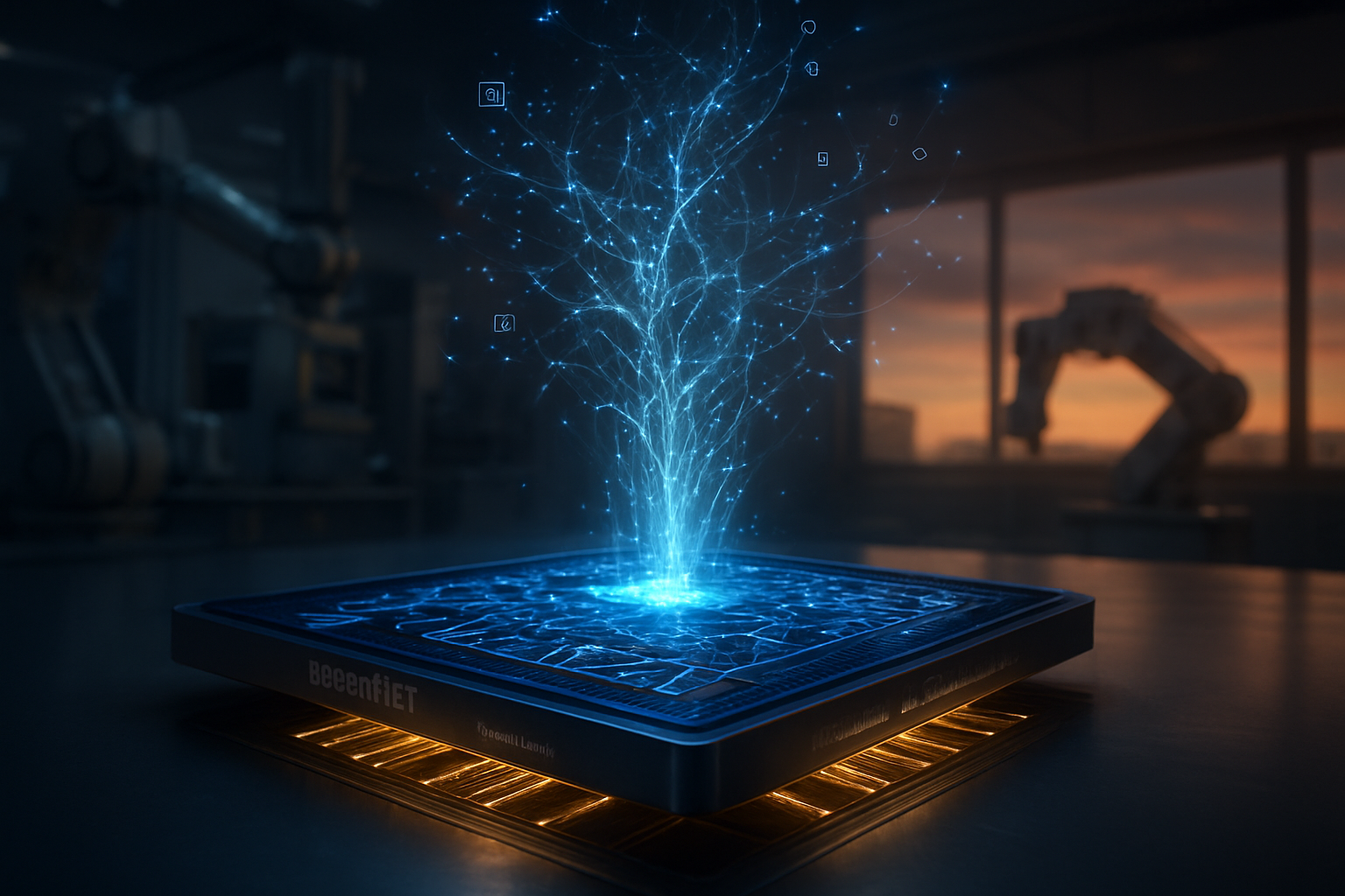
    At the 2026 Consumer Electronics Show (CES), NVIDIA (NASDAQ: NVDA) redefined the boundaries of artificial intelligence by unveiling the Nemotron 3 family of open models. Moving beyond the text-and-image paradigms of previous years, the new suite is specifically engineered for "agentic AI"—autonomous systems capable of multi-step reasoning, tool use, and complex decision-making. This launch marks a pivotal shift for the tech giant as it transitions from a provider of general-purpose large language models (LLMs) to the architect of a comprehensive "Physical AI" ecosystem.

    The announcement signals Nvidia's ambition to move AI off the screen and into the physical world. By integrating the Nemotron 3 reasoning engine with its newly announced Cosmos world foundation models and Rubin hardware platform, Nvidia is providing the foundational software and hardware stack for the next generation of humanoid robots, autonomous vehicles, and industrial automation systems. The immediate significance is clear: Nvidia is no longer just selling the "shovels" for the AI gold rush; it is now providing the brains and the bodies for the autonomous workforce of the future.

    Technical Mastery: The Hybrid Mamba-Transformer Architecture

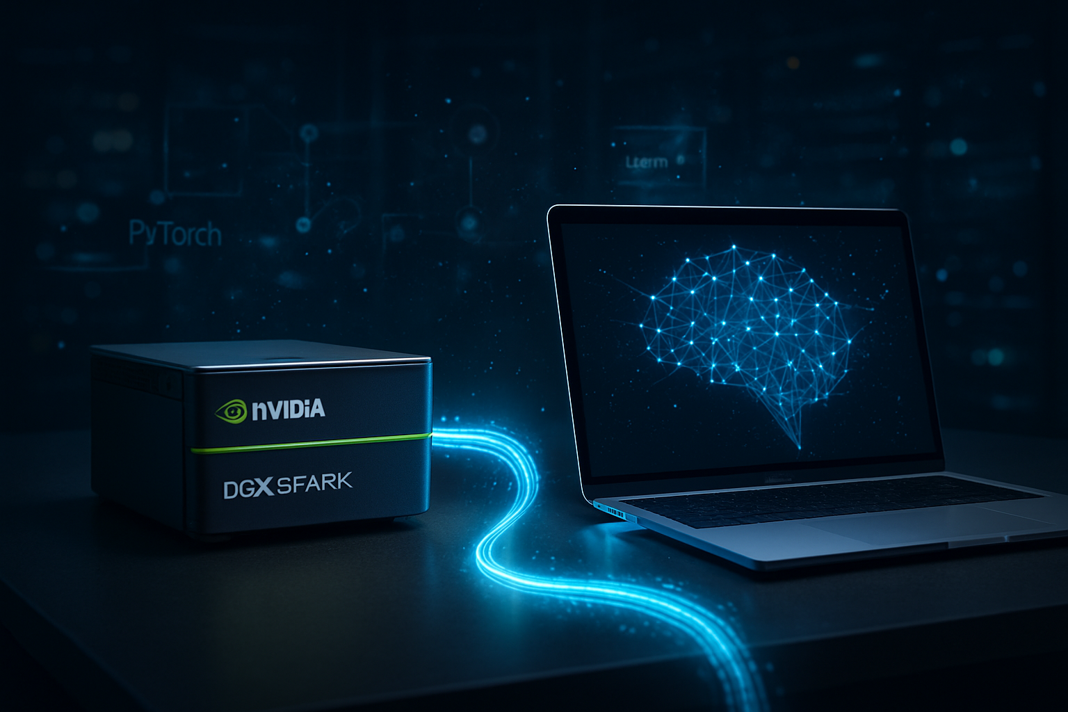
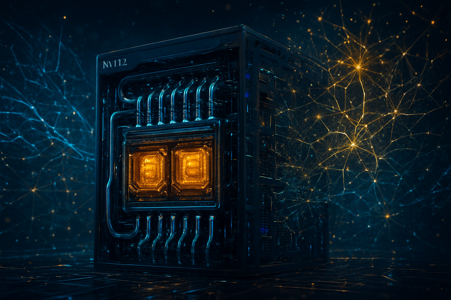
    The Nemotron 3 family represents a significant technical departure from the industry-standard Transformer-only models. Built on a sophisticated Hybrid Mamba-Transformer Mixture-of-Experts (MoE) architecture, these models combine the high-reasoning accuracy of Transformers with the low-latency and long-context efficiency of Mamba-2. The family is tiered into three primary sizes: the 30B Nemotron 3 Nano for local edge devices, the 100B Nemotron 3 Super for enterprise automation, and the massive 500B Nemotron 3 Ultra, which sets new benchmarks for complex scientific planning and coding.

    One of the most striking technical features is the massive 1-million-token context window, allowing agents to ingest and "remember" entire technical manuals or weeks of operational data in a single pass. Furthermore, Nvidia has introduced granular "Reasoning Controls," including a "Thinking Budget" that allows developers to toggle between high-speed responses and deep-reasoning modes. This flexibility is essential for agentic workflows where a robot might need to react instantly to a physical hazard but spend several seconds planning a complex assembly task. Initial reactions from the AI research community have been overwhelmingly positive, with experts noting that the 4x throughput increase over Nemotron 2, when paired with the new Rubin GPUs, effectively solves the latency bottleneck that previously plagued real-time agentic AI.

    Strategic Dominance: Reshaping the Competitive Landscape

    The release of Nemotron 3 as an open-model family places significant pressure on proprietary AI labs like OpenAI and Google (NASDAQ: GOOGL). By offering state-of-the-art (SOTA) reasoning capabilities that are optimized to run with maximum efficiency on Nvidia hardware, the company is incentivizing developers to build within its ecosystem rather than relying on closed APIs. This strategy directly benefits enterprise giants like Siemens (OTC: SIEGY), which has already announced plans to integrate Nemotron 3 into its industrial design software to create AI agents that assist in complex semiconductor and PCB layout.

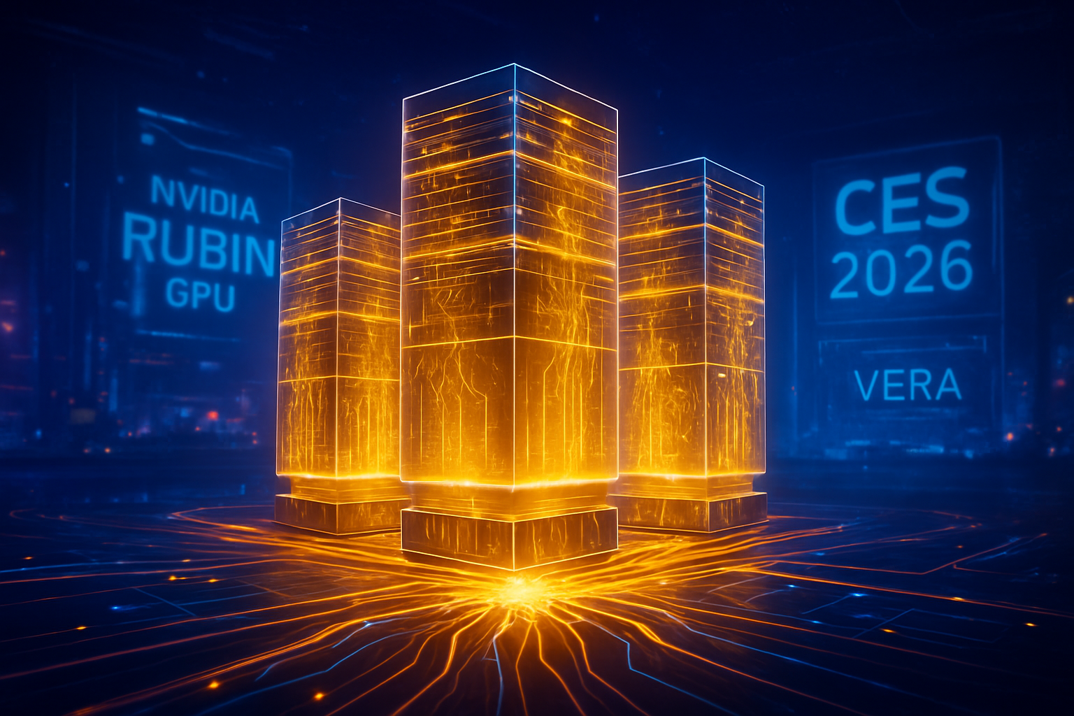
    For startups and smaller AI labs, the availability of these high-performance open models lowers the barrier to entry for developing sophisticated agents. However, the true competitive advantage lies in Nvidia's vertical integration. Because Nemotron 3 is specifically tuned for the Rubin platform—utilizing the new Vera CPU and BlueField-4 DPU for optimized data movement—competitors who lack integrated hardware stacks may find it difficult to match the performance-to-cost ratio Nvidia is now offering. This positioning turns Nvidia into a "one-stop shop" for Physical AI, potentially disrupting the market for third-party orchestration layers and middleware.

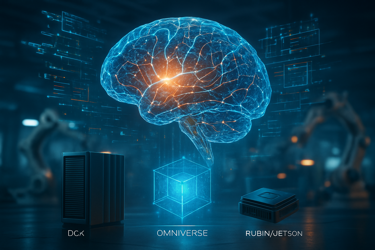
    The Physical AI Vision: Bridging the Digital-Physical Divide

    The "Physical AI" strategy announced at CES 2026 is perhaps the most ambitious roadmap in Nvidia's history. It is built on a "three-computer" architecture: the DGX for training, Omniverse for simulation, and Jetson or DRIVE for real-time operation. Within this framework, Nemotron 3 serves as the "logic" or the brain, while the new NVIDIA Cosmos models act as the "intuition." Cosmos models are world foundation models designed to understand physics—predicting how objects fall, slide, or interact—which allows robots to navigate the real world with human-like common sense.

    This integration is a milestone in the broader AI landscape, moving beyond the "stochastic parrot" critique of early LLMs. By grounding reasoning in physical reality, Nvidia is addressing one of the most significant hurdles in robotics: the "sim-to-real" gap. Unlike previous breakthroughs that focused on digital intelligence, such as GPT-4, the combination of Nemotron and Cosmos allows for "Physical Common Sense," where an AI doesn't just know how to describe a hammer but understands the weight, trajectory, and force required to use one. This shift places Nvidia at the forefront of the "General Purpose Robotics" trend that many believe will define the late 2020s.

    The Road Ahead: Humanoids and Autonomous Realities

    Looking toward the near-term future, the most immediate applications of the Nemotron-Cosmos stack will be seen in humanoid robotics and autonomous transport. Nvidia’s Isaac GR00T N1.6—a Vision-Language-Action (VLA) model—is already utilizing Nemotron 3 to enable robots to perform bimanual manipulation and navigate dynamic, crowded workspaces. In the automotive sector, the new Alpamayo 1 model, developed in partnership with Mercedes-Benz (OTC: MBGYY), uses Nemotron's chain-of-thought reasoning to allow self-driving cars to explain their decisions to passengers, such as slowing down for a distracted pedestrian.

    Despite the excitement, significant challenges remain, particularly regarding the safety and reliability of autonomous agents in unconstrained environments. Experts predict that the next two years will be focused on "alignment for action," ensuring that agentic AI follows strict safety protocols when interacting with humans. As these models become more autonomous, the industry will likely see a surge in demand for "Inference Context Memory Storage" and other hardware-level solutions to manage the massive data flows required by multi-agent systems.

    A New Chapter in the AI Revolution

    Nvidia’s announcements at CES 2026 represent a definitive closing of the chapter on "Chatbot AI" and the opening of the era of "Agentic Physical AI." The Nemotron 3 family provides the necessary reasoning depth, while the Cosmos models provide the physical grounding, creating a holistic system that can finally interact with the world in a meaningful way. This development is likely to be remembered as the moment when AI moved from being a tool we talk to, to a partner that works alongside us.

    As we move into the coming months, the industry will be watching closely to see how quickly these models are adopted by the robotics and automotive sectors. With the Rubin platform entering full production and partnerships with global leaders already in place, Nvidia has set a high bar for the rest of the tech industry. The long-term impact of this development could be a fundamental shift in global productivity, as autonomous agents begin to take on roles in manufacturing, logistics, and even domestic care that were once thought to be decades away.


    This content is intended for informational purposes only and represents analysis of current AI developments.

    TokenRing AI delivers enterprise-grade solutions for multi-agent AI workflow orchestration, AI-powered development tools, and seamless remote collaboration platforms.
    For more information, visit https://www.tokenring.ai/.

  • Nvidia’s CES 2026 Breakthrough: DGX Spark Update Turns MacBooks into AI Supercomputers

    Nvidia’s CES 2026 Breakthrough: DGX Spark Update Turns MacBooks into AI Supercomputers

    In a move that has sent shockwaves through the consumer and professional hardware markets, Nvidia (NASDAQ: NVDA) announced a transformative software update for its DGX Spark AI mini PC at CES 2026. The update effectively redefines the role of the compact supercomputer, evolving it from a standalone developer workstation into a high-octane external AI accelerator specifically optimized for Apple (NASDAQ: AAPL) MacBook Pro users. By bridging the gap between macOS portability and Nvidia's dominant CUDA ecosystem, the Santa Clara-based chip giant is positioning the DGX Spark as the essential "sidecar" for the next generation of AI development and creative production.

    The announcement marks a strategic pivot toward "Deskside AI," a movement aimed at bringing data-center-level compute power directly to the user’s desk without the latency or privacy concerns associated with cloud-based processing. With this update, Nvidia is not just selling hardware; it is offering a seamless "hybrid workflow" that allows developers and creators to offload the most grueling AI tasks—such as 4K video generation and large language model (LLM) fine-tuning—to a dedicated local node, all while maintaining the familiar interface of their primary laptop.

    The Technical Leap: Grace Blackwell and the End of the "VRAM Wall"

    The core of the DGX Spark's newfound capability lies in its internal architecture, powered by the GB10 Grace Blackwell Superchip. While the hardware remains the same as the initial launch, the 2026 software stack unlocks unprecedented efficiency through the introduction of NVFP4 quantization. This new numerical format allows the Spark to run massive models with significantly lower memory overhead, effectively doubling the performance of the device's 128GB of unified memory. Nvidia claims that these optimizations, combined with updated TensorRT-LLM kernels, provide a 2.5× performance boost over previous software versions.

    Perhaps the most impressive technical feat is the "Accelerator Mode" designed for the MacBook Pro. Utilizing high-speed local connectivity, the Spark can now act as a transparent co-processor for macOS. In a live demonstration at CES, Nvidia showed a MacBook Pro equipped with an M4 Max chip attempting to generate a high-fidelity video using the FLUX.1-dev model. While the MacBook alone required eight minutes to complete the task, offloading the compute to the DGX Spark reduced the processing time to just 60 seconds. This 8-fold speed increase is achieved by bypassing the thermal and power constraints of a laptop and utilizing the Spark’s 1 petaflop of AI throughput.

    Beyond raw speed, the update brings native, "out-of-the-box" support for the industry’s most critical open-source frameworks. This includes deep integration with PyTorch, vLLM, and llama.cpp. For the first time, Nvidia is providing pre-validated "Playbooks"—reference frameworks that allow users to deploy models from Meta (NASDAQ: META) and Stability AI with a single click. These optimizations are specifically tuned for the Llama 3 series and Stable Diffusion 3.5 Large, ensuring that the Spark can handle models with over 100 billion parameters locally—a feat previously reserved for multi-GPU server racks.

    Market Disruption: Nvidia’s Strategic Play for the Apple Ecosystem

    The decision to target the MacBook Pro is a calculated masterstroke. For years, AI developers have faced a difficult choice: the sleek hardware and Unix-based environment of a Mac, or the CUDA-exclusive performance of an Nvidia-powered PC. By turning the DGX Spark into a MacBook peripheral, Nvidia is effectively removing the primary reason for power users to leave the Apple ecosystem, while simultaneously ensuring that those users remain dependent on Nvidia’s software stack. This "best of both worlds" approach creates a powerful moat against competitors who are trying to build integrated AI PCs.

    This development poses a direct challenge to Intel (NASDAQ: INTC) and AMD (NASDAQ: AMD). While Intel’s "Panther Lake" Core Ultra Series 3 and AMD’s "Helios" AI mini PCs are making strides in NPU (Neural Processing Unit) performance, they lack the massive VRAM capacity and the specialized CUDA libraries that have become the industry standard for AI research. By positioning the $3,999 DGX Spark as a premium "accelerator," Nvidia is capturing the high-end market before its rivals can establish a foothold in the local AI workstation space.

    Furthermore, this move creates a complex dynamic for cloud providers like Amazon (NASDAQ: AMZN) and Microsoft (NASDAQ: MSFT). As the DGX Spark makes local inference and fine-tuning more accessible, the reliance on expensive cloud instances for R&D may diminish. Analysts suggest this could trigger a "Hybrid AI" shift, where companies use local Spark units for proprietary data and development, only scaling to AWS or Azure for massive-scale training or global deployment. In response, cloud giants are already slashing prices on Nvidia-based instances to prevent a mass migration to "deskside" hardware.

    Privacy, Sovereignty, and the Broader AI Landscape

    The wider significance of the DGX Spark update extends beyond mere performance metrics; it represents a major step toward "AI Sovereignty" for individual creators and small enterprises. By providing the tools to run frontier-class models like Llama 3 and Flux locally, Nvidia is addressing the growing concerns over data privacy and intellectual property. In an era where sending proprietary code or creative assets to a cloud-based AI can be a legal minefield, the ability to keep everything within a local, physical "box" is a significant selling point.

    This shift also highlights a growing trend in the AI landscape: the transition from "General AI" to "Agentic AI." Nvidia’s introduction of the "Local Nsight Copilot" within the Spark update allows developers to use a CUDA-optimized AI assistant that resides entirely on the device. This assistant can analyze local codebases and provide real-time optimizations without ever connecting to the internet. This "local-first" philosophy is a direct response to the demands of the AI research community, which has long advocated for more decentralized and private computing options.

    However, the move is not without its potential concerns. The high price point of the DGX Spark risks creating a "compute divide," where only well-funded researchers and elite creative studios can afford the hardware necessary to run the latest models at full speed. While Nvidia is democratizing access to high-end AI compared to data-center costs, the $3,999 entry fee remains a barrier for many independent developers, potentially centralizing power among those who can afford the "Nvidia Tax."

    The Road Ahead: Agentic Robotics and the Future of the Spark

    Looking toward the future, the DGX Spark update is likely just the beginning of Nvidia’s ambitions for small-form-factor AI. Industry experts predict that the next phase will involve "Physical AI"—the integration of the Spark as a brain for local robotic systems and autonomous agents. With its 128GB of unified memory and Blackwell architecture, the Spark is uniquely suited to handle the complex multi-modal inputs required for real-time robotic navigation and manipulation.

    We can also expect to see tighter integration between the Spark and Nvidia’s Omniverse platform. As AI-generated 3D content becomes more prevalent, the Spark could serve as a dedicated rendering and generation node for virtual worlds, allowing creators to build complex digital twins on their MacBooks with the power of a local supercomputer. The challenge for Nvidia will be maintaining this lead as Apple continues to beef up its own Unified Memory architecture and as AMD and Intel inevitably release more competitive "AI PC" silicon in the 2027-2028 timeframe.

    Final Thoughts: A New Chapter in Local Computing

    The CES 2026 update for the DGX Spark is more than just a software patch; it is a declaration of intent. By enabling the MacBook Pro to tap into the power of the Blackwell architecture, Nvidia has bridged one of the most significant divides in the tech world. The "VRAM wall" that once limited local AI development is crumbling, and the era of the "deskside supercomputer" has officially arrived.

    For the industry, the key takeaway is clear: the future of AI is hybrid. While the cloud will always have its place for massive-scale operations, the "center of gravity" for development and creative experimentation is shifting back to the local device. As we move into the middle of 2026, the success of the DGX Spark will be measured not just by units sold, but by the volume of innovative, locally-produced AI applications that emerge from this new synergy between Nvidia’s silicon and the world’s most popular professional laptops.


    This content is intended for informational purposes only and represents analysis of current AI developments.

    TokenRing AI delivers enterprise-grade solutions for multi-agent AI workflow orchestration, AI-powered development tools, and seamless remote collaboration platforms.
    For more information, visit https://www.tokenring.ai/.

  • CES 2026: Lenovo and Motorola Unveil ‘Qira,’ the Ambient AI Bridge That Finally Ends the Windows-Android Divide

    CES 2026: Lenovo and Motorola Unveil ‘Qira,’ the Ambient AI Bridge That Finally Ends the Windows-Android Divide

    At the 2026 Consumer Electronics Show (CES) in Las Vegas, Lenovo (HKG: 0992) and its subsidiary Motorola have fundamentally rewritten the rules of personal computing with the launch of Qira, a "Personal Ambient Intelligence" system. Moving beyond the era of standalone chatbots and fragmented apps, Qira represents the first truly successful attempt to create a seamless, context-aware AI layer that follows a user across their entire hardware ecosystem. Whether a user is transitioning from a Motorola smartphone to a Lenovo Yoga laptop or checking a wearable device, Qira maintains a persistent "neural thread," ensuring that digital context is never lost during device handoffs.

    The announcement, delivered at the high-tech Sphere venue, signals a pivot for the tech industry away from "Generative AI" as a destination and toward "Ambient Computing" as a lifestyle. By embedding Qira at the system level of both Windows and Android, Lenovo is positioning itself not just as a hardware manufacturer, but as the architect of a unified digital consciousness. This development marks a significant milestone in the evolution of the personal computer, transforming it from a passive tool into a proactive agent capable of managing complex life tasks—like trip planning and cross-device file management—without the user ever having to open a traditional application.

    The Technical Architecture of Ambient Intelligence

    Qira is built on a sophisticated Hybrid AI Architecture that balances local privacy with cloud-based reasoning. At its core, the system utilizes a "Neural Fabric" that orchestrates tasks between on-device Small Language Models (SLMs) and massive cloud-based Large Language Models (LLMs). For immediate, privacy-sensitive tasks, Qira employs Microsoft’s (NASDAQ: MSFT) Phi-4 mini, running locally on the latest NPU-heavy silicon. To handle the "full" ambient experience, Lenovo has mandated hardware capable of 40+ TOPS (Trillion Operations Per Second), specifically optimizing for the new Intel (NASDAQ: INTC) Core Ultra "Panther Lake" and Qualcomm (NASDAQ: QCOM) Snapdragon X2 processors.

    What distinguishes Qira from previous iterations of AI assistants is its "Fused Knowledge Base." Unlike Apple Intelligence, which focuses primarily on on-screen awareness, Qira observes user intent across different operating systems. Its flagship feature, "Next Move," proactively surfaces the files, browser tabs, and documents a user was working on their phone the moment they flip open their laptop. In technical demonstrations, Qira showcased its ability to perform point-to-point file transfers both online and offline, bypassing cloud intermediaries like Dropbox or email. By using a dedicated hardware "Qira Key" on PCs and a "Persistent Pill" UI on Motorola devices, the AI remains a constant, low-latency companion that understands the user’s physical and digital environment.

    Initial reactions from the AI research community have been overwhelmingly positive, with many praising the "Catch Me Up" feature. This tool provides a multimodal summary of missed notifications and activity across all linked devices, effectively acting as a personal secretary that filters noise from signal. Experts note that by integrating directly with the Windows Foundry and Android kernel, Lenovo has achieved a level of "neural sync" that third-party software developers have struggled to reach for decades.

    Strategic Implications and the "Context Wall"

    The launch of Qira places Lenovo in direct competition with the "walled gardens" of Apple Inc. (NASDAQ: AAPL) and Alphabet Inc. (NASDAQ: GOOGL). By bridging the gap between Windows and Android, Lenovo is attempting to create its own ecosystem lock-in, which analysts are calling the "Context Wall." Once Qira learns a user’s specific habits, professional tone, and travel preferences across their ThinkPad and Razr phone, the "switching cost" to another brand becomes immense. This strategy is designed to drive a faster PC refresh cycle, as the most advanced ambient features require the high-performance NPUs found in the newest 2026 models.

    For tech giants, the implications are profound. Microsoft benefits significantly from this partnership, as Qira utilizes the Azure OpenAI Service for its cloud-heavy reasoning, further cementing the Microsoft AI stack in the enterprise and consumer sectors. Meanwhile, Expedia Group (NASDAQ: EXPE) has emerged as a key launch partner, integrating its travel inventory directly into Qira’s agentic workflows. This allows Qira to plan entire vacations—booking flights, hotels, and local transport—based on a single conversational prompt or a photo found in the user's gallery, potentially disrupting the traditional "search and book" model of the travel industry.

    A Paradigm Shift Toward Ambient Computing

    Qira represents a broader shift in the AI landscape from "proactive" to "ambient." In this new era, the AI does not wait for a prompt; it exists in the background, sensing context through cameras, microphones, and sensor data. This fits into a trend where the interface becomes invisible. Lenovo’s Project Maxwell, a wearable AI pin showcased alongside Qira, illustrates this perfectly. The pin provides visual context to the AI, allowing it to "see" what the user sees, thereby enabling Qira to offer live translation or real-time advice during a physical meeting without the user ever touching a screen.

    However, this level of integration brings significant privacy concerns. The "Fused Knowledge Base" essentially creates a digital twin of the user’s life. While Lenovo emphasizes its hybrid approach—keeping the most sensitive "Personal Knowledge" on-device—the prospect of a system-level agent observing every keystroke and camera feed will likely face scrutiny from regulators and privacy advocates. Comparisons are already being drawn to previous milestones like the launch of the original iPhone or the debut of ChatGPT; however, Qira’s significance lies in its ability to make the technology disappear into the fabric of daily life.

    The Horizon: From Assistants to Agents

    Looking ahead, the evolution of Qira is expected to move toward even greater autonomy. In the near term, Lenovo plans to expand Qira’s "Agentic Workflows" to include more third-party integrations, potentially allowing the AI to manage financial portfolios or handle complex enterprise project management. The "ThinkPad Rollable XD," a concept laptop also revealed at CES, suggests a future where hardware physically adapts to the AI’s needs—expanding its screen real estate when Qira determines the user is entering a "deep work" phase.

    Experts predict that the next challenge for Lenovo will be the "iPhone Factor." To truly dominate, Lenovo must find a way to offer Qira’s best features to users who prefer iOS, a task that remains difficult due to Apple's restrictive ecosystem. Nevertheless, the development of "AI Glasses" and other wearables suggests that the battle for ambient supremacy will eventually move off the smartphone and onto the face and body, where Lenovo is already making significant experimental strides.

    Summary of the Ambient Era

    The launch of Qira at CES 2026 marks a definitive turning point in the history of artificial intelligence. By successfully unifying the Windows and Android experiences through a context-aware, ambient layer, Lenovo and Motorola have moved the industry past the "app-centric" model that has dominated for nearly two decades. The key takeaways from this launch are the move toward hybrid local/cloud processing, the rise of agentic travel and file management, and the creation of a "Context Wall" that prioritizes user history over raw hardware specs.

    As we move through 2026, the tech world will be watching closely to see how quickly consumers adopt these ambient features and whether competitors like Samsung or Dell can mount a convincing response. For now, Lenovo has seized the lead in the "Agency War," proving that in the future of computing, the most powerful tool is the one you don't even have to open.


    This content is intended for informational purposes only and represents analysis of current AI developments.

    TokenRing AI delivers enterprise-grade solutions for multi-agent AI workflow orchestration, AI-powered development tools, and seamless remote collaboration platforms.
    For more information, visit https://www.tokenring.ai/.

  • Intel Reclaims the Silicon Crown: Core Ultra Series 3 ‘Panther Lake’ Debuts at CES 2026 as First US-Made 18A AI PC Chip

    Intel Reclaims the Silicon Crown: Core Ultra Series 3 ‘Panther Lake’ Debuts at CES 2026 as First US-Made 18A AI PC Chip

    In a landmark moment for the global semiconductor industry, Intel (NASDAQ:INTC) officially launched its Core Ultra Series 3 processors, codenamed "Panther Lake," at CES 2026. Unveiled by senior leadership at the Las Vegas tech showcase, Panther Lake represents more than just a seasonal hardware refresh; it is the first consumer-grade silicon built on the Intel 18A process node, manufactured entirely within the United States. This launch marks the culmination of Intel’s ambitious "five nodes in four years" strategy, signaling a definitive return to the forefront of manufacturing technology.

    The immediate significance of Panther Lake lies in its role as the engine for the next generation of "Agentic AI PCs." With a dedicated Neural Processing Unit (NPU) delivering 50 TOPS (Trillions of Operations Per Second) and a total platform throughput of 180 TOPS, Intel is positioning these chips to handle complex, autonomous AI agents locally on the device. By combining cutting-edge domestic manufacturing with unprecedented AI performance, Intel is not only challenging its rivals but also reinforcing the strategic importance of a resilient, US-based semiconductor supply chain.

    The 18A Breakthrough: RibbonFET and PowerVia Take Center Stage

    Technically, Panther Lake is a marvel of modern engineering, representing the first large-scale implementation of two foundational innovations: RibbonFET and PowerVia. RibbonFET is Intel’s implementation of a gate-all-around (GAA) transistor architecture, which replaces the long-standing FinFET design. This allows for better electrostatic control and higher drive current at lower voltages, resulting in a 15% improvement in performance-per-watt over previous generations. Complementing this is PowerVia, the industry's first backside power delivery system. By moving power routing to the back of the wafer, Intel has eliminated traditional bottlenecks in transistor density and reduced voltage droop, allowing the chip to run more efficiently under heavy AI workloads.

    At the heart of Panther Lake’s AI capabilities is the NPU 5 architecture. While the previous generation "Lunar Lake" met the 40 TOPS threshold for Microsoft (NASDAQ:MSFT) Copilot+ certification, Panther Lake pushes the dedicated NPU to 50 TOPS. When the NPU works in tandem with the new Xe3 "Celestial" graphics architecture and the high-performance Cougar Cove CPU cores, the total platform performance reaches a staggering 180 TOPS. This leap is specifically designed to enable "Small Language Models" (SLMs) and vision-action models to run with near-zero latency, allowing for real-time privacy-focused AI assistants that don't rely on the cloud.

    The integrated graphics also see a massive overhaul. The Xe3 Celestial architecture, marketed under the Arc B-Series umbrella, features up to 12 Xe3 cores. Intel claims this provides a 77% increase in gaming performance compared to the Core Ultra 9 285H. Beyond gaming, these GPU cores are equipped with XMX engines that provide the bulk of the platform’s 180 TOPS, making the chip a powerhouse for local generative AI tasks like image creation and video upscaling.

    Initial reactions from the industry have been overwhelmingly positive. Analysts from the AI research community have noted that Panther Lake’s focus on "total platform TOPS" rather than just NPU throughput reflects a more mature understanding of how AI software actually utilizes hardware. By spreading the load across the CPU, GPU, and NPU, Intel is providing developers with a more flexible playground for building the next generation of software.

    Reshaping the Competitive Landscape: Intel vs. The World

    The launch of Panther Lake creates immediate pressure on Intel’s primary competitors: AMD (NASDAQ:AMD), Qualcomm (NASDAQ:QCOM), and Apple (NASDAQ:AAPL). While Qualcomm’s Snapdragon X2 Elite currently holds the lead in raw NPU throughput with 80 TOPS, Intel’s "total platform" approach and superior integrated graphics offer a more balanced package for power users and gamers. AMD’s Ryzen AI 400 series, also debuting at CES 2026, competes closely with a 60 TOPS NPU, but Intel’s transition to the 18A node gives it a density and power efficiency advantage that AMD, still largely reliant on TSMC (NYSE:TSM) for manufacturing, may struggle to match in the short term.

    For tech giants like Dell (NYSE:DELL), HP (NYSE:HPQ), and ASUS, Panther Lake provides the high-performance silicon needed to justify a new upgrade cycle for enterprise and consumer laptops. These manufacturers have already announced over 200 designs based on the new architecture, many of which focus on "AI-first" features like automated workflow orchestration and real-time multi-modal translation. The ability to run these tasks locally reduces cloud costs for enterprises, making Intel-powered AI PCs an attractive proposition for IT departments.

    Furthermore, the success of the 18A node is a massive win for the Intel Foundry business. With Panther Lake proving that 18A is ready for high-volume production, external customers like Amazon (NASDAQ:AMZN) and the U.S. Department of Defense are likely to accelerate their own 18A-based projects. This positions Intel not just as a chip designer, but as a critical manufacturing partner for the entire tech industry, potentially disrupting the long-standing dominance of TSMC in the leading-edge foundry market.

    A Geopolitical Milestone: The Return of US Silicon Leadership

    Beyond the spec sheets, Panther Lake carries immense weight in the broader context of global technology and geopolitics. For the first time in over a decade, the world’s most advanced semiconductor process node is being manufactured in the United States, specifically at Intel’s Fab 52 in Arizona. This is a direct victory for the CHIPS and Science Act, which sought to revitalize domestic manufacturing and reduce reliance on overseas supply chains.

    The strategic importance of this cannot be overstated. As AI becomes a central pillar of national security and economic competitiveness, having a domestic source of leading-edge AI silicon is a critical advantage. The U.S. government’s involvement through the RAMP-C project ensures that the same 18A technology powering consumer laptops will also underpin the next generation of secure defense systems.

    However, this shift also brings concerns regarding the sustainability of such massive energy requirements. The production of 18A chips involves High-NA EUV lithography, a process that is incredibly energy-intensive. As Intel scales this production, the industry will be watching closely to see how the company balances its manufacturing ambitions with its environmental and social governance (ESG) goals. Nevertheless, compared to previous milestones like the introduction of the first 64-bit processors or the shift to multi-core architectures, the move to 18A and integrated AI represents a more fundamental shift in how computing power is generated and deployed.

    The Horizon: From AI PCs to Autonomous Systems

    Looking ahead, Panther Lake is just the beginning of Intel’s 18A journey. The company has already teased its next-generation "Clearwater Forest" Xeon processors for data centers and the future "14A" node, which is expected to push boundaries even further by 2027. In the near term, we can expect to see a surge in "Agentic" software—applications that don't just respond to prompts but proactively manage tasks for the user. With 50+ TOPS of NPU power, these agents will be able to "see" what is on a user's screen and "act" across different applications securely and privately.

    The challenges remaining are largely on the software side. While the hardware is now capable of 180 TOPS, the ecosystem of developers must catch up to utilize this power effectively. We expect to see Microsoft release a major Windows "AI Edition" update later this year that specifically targets the capabilities of Panther Lake and its contemporaries, potentially moving the operating system's core functions into the AI domain.

    Closing the Chapter on the "Foundry Gap"

    In summary, the launch of the Core Ultra Series 3 "Panther Lake" at CES 2026 is a defining moment for Intel and the American tech industry. By successfully delivering a 1.8nm-class processor with a 50 TOPS NPU and high-end integrated graphics, Intel has proved that it can still innovate at the bleeding edge of physics. The 18A node is no longer a roadmap promise; it is a shipping reality that re-establishes Intel as a formidable leader in both chip design and manufacturing.

    As we move into the first quarter of 2026, the industry will be watching the retail performance of these chips and the stability of the 18A yields. If Intel can maintain this momentum, the "Foundry Gap" that has defined the last five years of the semiconductor industry may finally be closed. For now, the AI PC has officially entered its most powerful era yet, and for the first time in a long time, the heart of that innovation is beating in the American Southwest.


    This content is intended for informational purposes only and represents analysis of current AI developments.

    TokenRing AI delivers enterprise-grade solutions for multi-agent AI workflow orchestration, AI-powered development tools, and seamless remote collaboration platforms.
    For more information, visit https://www.tokenring.ai/.

  • The HBM4 Memory War: SK Hynix, Samsung, and Micron Clash at CES 2026 to Power NVIDIA’s Rubin Revolution

    The HBM4 Memory War: SK Hynix, Samsung, and Micron Clash at CES 2026 to Power NVIDIA’s Rubin Revolution

    The 2026 Consumer Electronics Show (CES) in Las Vegas has transformed from a showcase of consumer gadgets into the primary battlefield for the most critical component in the artificial intelligence era: High Bandwidth Memory (HBM). As of January 8, 2026, the industry is witnessing the eruption of the "HBM4 Memory War," a high-stakes conflict between the world’s three largest memory manufacturers—SK Hynix (KRX: 000660), Samsung Electronics (KRX: 005930), and Micron Technology (NASDAQ: MU). This technological arms race is not merely about storage; it is a desperate sprint to provide the massive data throughput required by NVIDIA’s (NASDAQ: NVDA) newly detailed "Rubin" platform, the successor to the record-breaking Blackwell architecture.

    The significance of this development cannot be overstated. As AI models grow to trillions of parameters, the bottleneck has shifted from raw compute power to memory bandwidth and energy efficiency. The announcements made this week at CES 2026 signal a fundamental shift in semiconductor architecture, where memory is no longer a passive storage bin but an active, logic-integrated component of the AI processor itself. With billions of dollars in capital expenditure on the line, the winners of this HBM4 cycle will likely dictate the pace of AI advancement for the remainder of the decade.

    Technical Frontiers: 16-Layer Stacks and the 1c Process

    The technical specifications unveiled at CES 2026 represent a monumental leap over the previous HBM3E standard. SK Hynix stole the early headlines by debuting the world’s first 16-layer 48GB HBM4 module. To achieve this, the company utilized its proprietary Advanced Mass Reflow Molded Underfill (MR-MUF) technology, thinning individual DRAM wafers to a staggering 30 micrometers to fit within the strict 775µm height limit set by JEDEC. This 16-layer stack delivers an industry-leading data rate of 11.7 Gbps per pin, which, when integrated into an 8-stack system like NVIDIA’s Rubin, provides a system-level bandwidth of 22 TB/s—nearly triple that of early HBM3E systems.

    Samsung Electronics countered with a focus on manufacturing sophistication and efficiency. Samsung’s HBM4 is built on its "1c" nanometer process (the 6th generation of 10nm-class DRAM). By moving to this advanced node, Samsung claims a 40% improvement in energy efficiency over its competitors. This is a critical advantage for data center operators struggling with the thermal demands of GPUs that now exceed 1,000 watts. Unlike its rivals, Samsung is leveraging its internal foundry to produce the HBM4 logic base die using a 10nm logic process, positioning itself as a "one-stop shop" that controls the entire stack from the silicon to the final packaging.

    Micron Technology, meanwhile, showcased its aggressive capacity expansion and its role as a lead partner for the initial Rubin launch. Micron’s HBM4 entry focuses on a 12-high (12-Hi) 36GB stack that emphasizes a 2048-bit interface—double the width of HBM3E. This allows for speeds exceeding 2.0 TB/s per stack while maintaining a 20% power efficiency gain over previous generations. The industry reaction has been one of collective awe; experts from the AI research community note that the shift from memory-based nodes to logic nodes (like TSMC’s 5nm for the base die) effectively turns HBM4 into a "custom" memory solution that can be tailored for specific AI workloads.

    The Kingmaker: NVIDIA’s Rubin Platform and the Supply Chain Scramble

    The primary driver of this memory frenzy is NVIDIA’s Rubin platform, which was the centerpiece of the CES 2026 keynote. The Rubin R100 and R200 GPUs, built on TSMC’s (NYSE: TSM) 3nm process, are designed to consume HBM4 at an unprecedented scale. Each Rubin GPU is expected to utilize eight stacks of HBM4, totaling 288GB of memory per chip. To ensure it does not repeat the supply shortages that plagued the Blackwell launch, NVIDIA has reportedly secured massive capacity commitments from all three major vendors, effectively acting as the kingmaker in the semiconductor market.

    Micron has responded with the most aggressive capacity expansion in its history, targeting a dedicated HBM4 production capacity of 15,000 wafers per month by the end of 2026. This is part of a broader $20 billion capital expenditure plan that includes new facilities in Taiwan and a "megaplant" in Hiroshima, Japan. By securing such a large slice of the Rubin supply chain, Micron is moving from its traditional "third-place" position to a primary supplier status, directly challenging the dominance of SK Hynix.

    The competitive implications extend beyond the memory makers. For AI labs and tech giants like Google (NASDAQ: GOOGL), Meta (NASDAQ: META), and Microsoft (NASDAQ: MSFT), the availability of HBM4-equipped Rubin GPUs will determine their ability to train next-generation "Agentic AI" models. Companies that can secure early allocations of these high-bandwidth systems will have a strategic advantage in inference speed and cost-per-query, potentially disrupting existing SaaS products that are currently limited by the latency of older hardware.

    A Paradigm Shift: From Compute-Centric to Memory-Centric AI

    The "HBM4 War" marks a broader shift in the AI landscape. For years, the industry focused on "Teraflops"—the number of floating-point operations a processor could perform. However, as models have grown, the energy cost of moving data between the processor and memory has become the primary constraint. The integration of logic dies into HBM4, particularly through the SK Hynix and TSMC "One-Team" alliance, signifies the end of the compute-only era. By embedding memory controllers and physical layer interfaces directly into the memory stack, manufacturers are reducing the physical distance data must travel, thereby slashing latency and power consumption.

    This development also brings potential concerns regarding market consolidation. The technical complexity and capital requirements of HBM4 are so high that smaller players are being priced out of the market entirely. We are seeing a "triopoly" where SK Hynix, Samsung, and Micron hold all the cards. Furthermore, the reliance on advanced packaging techniques like Hybrid Bonding and MR-MUF creates a new set of manufacturing risks; any yield issues at these nanometer scales could lead to global shortages of AI hardware, stalling progress in fields from drug discovery to climate modeling.

    Comparisons are already being drawn to the 2023 "GPU shortage," but with a twist. While 2023 was about the chips themselves, 2026 is about the interconnects and the stacking. The HBM4 breakthrough is arguably more significant than the jump from H100 to B100, as it addresses the fundamental "memory wall" that has threatened to plateau AI scaling laws.

    The Horizon: Rubin Ultra and the Road to 1TB Per GPU

    Looking ahead, the roadmap for HBM4 is already extending into 2027 and beyond. During the CES presentations, hints were dropped regarding the "Rubin Ultra" refresh, which is expected to move to 16-high HBM4e (Extended) stacks. This would effectively double the memory capacity again, potentially allowing for 1 terabyte of HBM memory on a single GPU package. Micron and SK Hynix are already sampling these 16-Hi stacks, with mass production targets set for early 2027.

    The next major challenge will be the move to "Custom HBM" (cHBM), where AI companies like OpenAI or Tesla (NASDAQ: TSLA) may design their own proprietary logic dies to be manufactured by TSMC and then stacked with DRAM by SK Hynix or Micron. This level of vertical integration would allow for AI-specific optimizations that are currently impossible with off-the-shelf components. Experts predict that by 2028, the distinction between "processor" and "memory" will have blurred so much that we may begin referring to them as unified "AI Compute Cubes."

    Final Reflections on the Memory-First Era

    The events at CES 2026 have made one thing clear: the future of artificial intelligence is being written in the cleanrooms of memory fabs. SK Hynix’s 16-layer breakthrough, Samsung’s 1c process efficiency, and Micron’s massive capacity ramp-up for NVIDIA’s Rubin platform collectively represent a new chapter in semiconductor history. We have moved past the era of general-purpose computing into a period of extreme specialization, where the ability to move data is as important as the ability to process it.

    As we move into the first quarter of 2026, the industry will be watching for the first production yields of these HBM4 modules. The success of the Rubin platform—and by extension, the next leap in AI capability—depends entirely on whether these three memory giants can deliver on their ambitious promises. For now, the "Memory War" is in full swing, and the spoils of victory are nothing less than the foundation of the global AI economy.


    This content is intended for informational purposes only and represents analysis of current AI developments.

    TokenRing AI delivers enterprise-grade solutions for multi-agent AI workflow orchestration, AI-powered development tools, and seamless remote collaboration platforms.
    For more information, visit https://www.tokenring.ai/.

  • AMD Shakes Up CES 2026 with Ryzen AI 400 and Ryzen AI Max: The New Frontier of 60 TOPS Edge Computing

    AMD Shakes Up CES 2026 with Ryzen AI 400 and Ryzen AI Max: The New Frontier of 60 TOPS Edge Computing

    In a definitive bid to capture the rapidly evolving "AI PC" market, Advanced Micro Devices (NASDAQ: AMD) took center stage at CES 2026 to unveil its next-generation silicon: the Ryzen AI 400 series and the powerhouse Ryzen AI Max processors. These announcements represent a pivotal shift in AMD’s strategy, moving beyond mere incremental CPU upgrades to deliver specialized silicon designed to handle the massive computational demands of local Large Language Models (LLMs) and autonomous "Physical AI" systems.

    The significance of these launches cannot be overstated. As the industry moves away from a total reliance on cloud-based AI, the Ryzen AI 400 and Ryzen AI Max are positioned as the primary engines for the next generation of "Copilot+" experiences. By integrating high-performance Zen 5 cores with a significantly beefed-up Neural Processing Unit (NPU), AMD is not just competing with traditional rival Intel; it is directly challenging NVIDIA (NASDAQ: NVDA) for dominance in the edge AI and workstation sectors.

    Technical Prowess: Zen 5 and the 60 TOPS Milestone

    The star of the show, the Ryzen AI 400 series (codenamed "Gorgon Point"), is built on a refined 4nm process and utilizes the Zen 5 microarchitecture. The flagship of this lineup, the Ryzen AI 9 HX 475, introduces the second-generation XDNA 2 NPU, which has been clocked to deliver a staggering 60 TOPS (Trillions of Operations Per Second). This marks a 20% increase over the previous generation and comfortably surpasses the 40-50 TOPS threshold required for the latest Microsoft Copilot+ features. This performance boost is achieved through a mix of high-performance Zen 5 cores and efficiency-focused Zen 5c cores, allowing thin-and-light laptops to maintain long battery life while processing complex AI tasks locally.

    For the professional and enthusiast market, the Ryzen AI Max series (codenamed "Strix Halo") pushes the boundaries of what integrated silicon can achieve. These chips, such as the Ryzen AI Max+ 392, feature up to 12 Zen 5 cores paired with a massive 40-core RDNA 3.5 integrated GPU. While the NPU in the Max series holds steady at 50 TOPS, its true power lies in its graphics-based AI compute—capable of up to 60 TFLOPS—and support for up to 128GB of LPDDR5X unified memory. This unified memory architecture is a direct response to the needs of AI developers, enabling the local execution of LLMs with up to 200 billion parameters, a feat previously impossible without high-end discrete graphics cards.

    This technical leap differs from previous approaches by focusing heavily on "balanced throughput." Rather than just chasing raw CPU clock speeds, AMD has optimized the interconnects between the Zen 5 cores, the RDNA 3.5 GPU, and the XDNA 2 NPU. Early reactions from industry experts suggest that AMD has successfully addressed the "memory bottleneck" that has plagued mobile AI performance. Analysts at the event noted that the ability to run massive models locally on a laptop-sized chip significantly reduces latency and enhances privacy, making these processors highly attractive for enterprise and creative workflows.

    Disrupting the Status Quo: A Direct Challenge to NVIDIA and Intel

    The introduction of the Ryzen AI Max series is a strategic shot across the bow for NVIDIA's workstation dominance. AMD explicitly positioned its new "Ryzen AI Halo" developer platforms as rivals to NVIDIA’s DGX Spark mini-workstations. By offering superior "tokens-per-second-per-dollar" for local LLM inference, AMD is targeting the growing demographic of AI researchers and developers who require powerful local hardware but may be priced out of NVIDIA’s high-end discrete GPU ecosystem. This competitive pressure could force a pricing realignment in the professional workstation market.

    Furthermore, AMD’s push into the edge and industrial sectors with the Ryzen AI Embedded P100 and X100 series directly challenges the NVIDIA Jetson lineup. These chips are designed for automotive digital cockpits and humanoid robotics, featuring industrial-grade temperature tolerances and a unified software stack. For tech giants like Tesla or robotics startups, the availability of a high-performance, X86-compatible alternative to ARM-based NVIDIA solutions provides more flexibility in software development and deployment.

    Major PC manufacturers, including Dell, HP, and Lenovo, have already announced dozens of designs based on the Ryzen AI 400 series. These companies stand to benefit from a renewed consumer interest in AI-capable hardware, potentially sparking a massive upgrade cycle. Meanwhile, Intel (NASDAQ: INTC) finds itself in a defensive position; while its "Panther Lake" chips offer competitive NPU performance, AMD’s lead in integrated graphics and unified memory for the workstation segment gives it a strategic advantage in the high-margin "Prosumer" market.

    The Broader AI Landscape: From Cloud to Edge

    AMD’s CES 2026 announcements reflect a broader trend in the AI landscape: the decentralization of intelligence. For the past several years, the "AI boom" has been characterized by massive data centers and cloud-based API calls. However, concerns over data privacy, latency, and the sheer cost of cloud compute have driven a demand for local execution. By delivering 60 TOPS in a thin-and-light form factor, AMD is making "Personal AI" a reality, where sensitive data never has to leave the user's device.

    This shift has profound implications for software development. With the release of ROCm 7.2, AMD is finally bringing its professional-grade AI software stack to the consumer and edge levels. This move aims to erode NVIDIA’s "CUDA moat" by providing an open-source, cross-platform alternative that works seamlessly across Windows and Linux. If AMD can successfully convince developers to optimize for ROCm at the edge, it could fundamentally change the power dynamics of the AI software ecosystem, which has been dominated by NVIDIA for over a decade.

    However, this transition is not without its challenges. The industry still lacks a unified standard for AI performance measurement, and "TOPS" can often be a misleading metric if the software cannot efficiently utilize the hardware. Comparisons to previous milestones, such as the transition to multi-core processing in the mid-2000s, suggest that we are currently in a "Wild West" phase of AI hardware, where architectural innovation is outpacing software standardization.

    The Horizon: What Lies Ahead for Ryzen AI

    Looking forward, the near-term focus for AMD will be the successful rollout of the Ryzen AI 400 series in Q1 2026. The real test will be the performance of these chips in real-world "Physical AI" applications. We expect to see a surge in specialized laptops and mini-PCs designed specifically for local AI training and "fine-tuning," where users can take a base model and customize it with their own data without needing a server farm.

    In the long term, the Ryzen AI Max series could pave the way for a new category of "AI-First" devices. Experts predict that by 2027, the distinction between a "laptop" and an "AI workstation" will blur, as unified memory architectures become the standard. The potential for these chips to power sophisticated humanoid robotics and autonomous vehicles is also on the horizon, provided AMD can maintain its momentum in the embedded space. The next major hurdle will be the integration of even more advanced "Agentic AI" capabilities directly into the silicon, allowing the NPU to proactively manage complex workflows without user intervention.

    Final Reflections on AMD’s AI Evolution

    AMD’s performance at CES 2026 marks a significant milestone in the company’s history. By successfully integrating Zen 5, RDNA 3.5, and XDNA 2 into a cohesive and powerful package, they have transitioned from a "CPU company" to a "Total AI Silicon company." The Ryzen AI 400 and Ryzen AI Max series are not just products; they are a statement of intent that AMD is ready to lead the charge into the era of pervasive, local artificial intelligence.

    The significance of this development in AI history lies in the democratization of high-performance compute. By bringing 60 TOPS and massive unified memory to the consumer and professional edge, AMD is lowering the barrier to entry for AI innovation. In the coming weeks and months, the tech world will be watching closely as the first Ryzen AI 400 systems hit the shelves and developers begin to push the limits of ROCm 7.2. The battle for the edge has officially begun, and AMD has just claimed a formidable piece of the high ground.


    This content is intended for informational purposes only and represents analysis of current AI developments.

    TokenRing AI delivers enterprise-grade solutions for multi-agent AI workflow orchestration, AI-powered development tools, and seamless remote collaboration platforms.
    For more information, visit https://www.tokenring.ai/.

  • Intel Reclaims the Silicon Crown: Core Ultra Series 3 “Panther Lake” Debuts at CES 2026

    Intel Reclaims the Silicon Crown: Core Ultra Series 3 “Panther Lake” Debuts at CES 2026

    LAS VEGAS — In a landmark moment for the American semiconductor industry, Intel (NASDAQ: INTC) officially launched its Core Ultra Series 3 processors, codenamed "Panther Lake," at CES 2026. This release marks the first consumer platform built on the highly anticipated Intel 18A process, representing the culmination of CEO Pat Gelsinger’s "five nodes in four years" strategy and a bold bid to regain undisputed process leadership from global rivals.

    The announcement is being hailed as a watershed event for both the AI PC market and domestic manufacturing. By bringing the world’s most advanced semiconductor process to high-volume production on U.S. soil, Intel is not just launching a new chip; it is attempting to shift the center of gravity for the global tech supply chain back to North America.

    The Engineering Marvel of 18A: RibbonFET and PowerVia

    Panther Lake is defined by its underlying manufacturing technology, Intel 18A, which introduces two foundational innovations to the market for the first time. The first is RibbonFET, Intel’s implementation of Gate-All-Around (GAA) transistor architecture. Unlike the FinFET designs that have dominated the industry for a decade, RibbonFET wraps the gate entirely around the channel, providing superior electrostatic control and significantly reducing power leakage. This allows for faster switching speeds in a smaller footprint, which Intel claims delivers a 15% performance-per-watt improvement over its predecessor.

    The second, and perhaps more revolutionary, innovation is PowerVia. This is the industry’s first implementation of backside power delivery, a technique that moves the power routing from the top of the silicon wafer to the bottom. By separating power and signal wires, Intel has eliminated the "wiring congestion" that has plagued chip designers for years. Initial benchmarks suggest this architectural shift improves cell utilization by nearly 10%, allowing the Core Ultra Series 3 to sustain higher clock speeds without the thermal throttling seen in previous generations.

    On the AI front, Panther Lake introduces the NPU 5 architecture, a dedicated neural processing unit capable of 50 Trillion Operations Per Second (TOPS). When combined with the new Xe3 "Celestial" graphics tiles and the high-performance CPU cores, the total platform throughput reaches a staggering 180 TOPS. This level of local compute power enables real-time execution of complex Vision-Language-Action (VLA) models and large language models (LLMs) like Llama 3 directly on the device, reducing the need for cloud-based AI processing and enhancing user privacy.

    A New Competitive Front in the Silicon Wars

    The launch of Panther Lake sets the stage for a brutal confrontation with Taiwan Semiconductor Manufacturing Company (NYSE: TSM). While TSMC is also ramping up its 2nm (N2) process, Intel's 18A is the first to market with backside power delivery—a feature TSMC isn't expected to implement in high volume until its N2P node later in 2026 or 2027. This technical head-start gives Intel a strategic window to court major fabless customers who are looking for the most efficient AI silicon.

    For competitors like Advanced Micro Devices (NASDAQ: AMD) and Qualcomm (NASDAQ: QCOM), the pressure is mounting. AMD’s upcoming Zen 6 architecture and Qualcomm’s next-generation Snapdragon X Elite chips will now be measured against the efficiency gains of Intel’s PowerVia. Furthermore, the massive 77% leap in gaming performance provided by Intel's Xe3 graphics architecture threatens to disrupt the low-to-midrange discrete GPU market, potentially impacting NVIDIA (NASDAQ: NVDA) as integrated graphics become "good enough" for the majority of mainstream gamers and creators.

    Market analysts suggest that Intel’s aggressive move into the 1.8nm-class era is as much about its foundry business as it is about its own chips. By proving that 18A can yield high-performance consumer silicon at scale, Intel is sending a clear signal to potential foundry customers like Microsoft (NASDAQ: MSFT) and Amazon (NASDAQ: AMZN) that it is a viable, cutting-edge alternative to TSMC for their custom AI accelerators.

    The Geopolitical and Economic Significance of U.S. Manufacturing

    Beyond the specs, the "Made in USA" badge on Panther Lake carries immense weight. The compute tiles for the Core Ultra Series 3 are being manufactured at Fab 52 in Chandler, Arizona, with advanced packaging taking place in Rio Rancho, New Mexico. This makes Panther Lake the most advanced semiconductor product ever mass-produced in the United States, a feat supported by significant investment and incentives from the CHIPS and Science Act.

    This domestic manufacturing capability addresses growing concerns over supply chain resilience and the concentration of advanced chipmaking in East Asia. For the U.S. government and domestic tech giants, Intel 18A represents a critical step toward "technological sovereignty." However, the transition has not been without its critics. Some industry observers point out that while the compute tiles are domestic, Intel still relies on TSMC for certain GPU and I/O tiles in the Panther Lake "disaggregated" design, highlighting the persistent interconnectedness of the global semiconductor industry.

    The broader AI landscape is also shifting. As "AI PCs" become the standard rather than the exception, the focus is moving away from raw TOPS and toward "TOPS-per-watt." Intel’s claim of 27-hour battery life in premium ultrabooks suggests that the 18A process has finally solved the efficiency puzzle that allowed Apple (NASDAQ: AAPL) and its ARM-based silicon to dominate the laptop market for the past several years.

    Looking Ahead: The Road to 14A and Beyond

    While Panther Lake is the star of CES 2026, Intel is already looking toward the horizon. The company has confirmed that its next-generation server chip, Clearwater Forest, is already in the sampling phase on 18A, and the successor to Panther Lake—codenamed Nova Lake—is expected to push the boundaries of AI integration even further in 2027.

    The next major milestone will be the transition to Intel 14A, which will introduce High-Numerical Aperture (High-NA) EUV lithography. This will be the next great battlefield in the quest for "Angstrom-era" silicon. The primary challenge for Intel moving forward will be maintaining high yields on these increasingly complex nodes. If the 18A ramp stays on track, experts predict Intel could regain the crown for the highest-performing transistors in the industry by the end of the year, a position it hasn't held since the mid-2010s.

    A Turning Point for the Silicon Giant

    The launch of the Core Ultra Series 3 "Panther Lake" is more than just a product refresh; it is a declaration of intent. By successfully deploying RibbonFET and PowerVia on the 18A node, Intel has demonstrated that it can still innovate at the bleeding edge of physics. The 180 TOPS of AI performance and the promise of "all-day-plus" battery life position the AI PC as the central tool for the next decade of productivity.

    As the first units begin shipping to consumers on January 27, the industry will be watching closely to see if Intel can translate this technical lead into market share gains. For now, the message from Las Vegas is clear: the silicon crown is back in play, and for the first time in a generation, the most advanced chips in the world are being forged in the American desert.


    This content is intended for informational purposes only and represents analysis of current AI developments.

    TokenRing AI delivers enterprise-grade solutions for multi-agent AI workflow orchestration, AI-powered development tools, and seamless remote collaboration platforms.
    For more information, visit https://www.tokenring.ai/.

  • NVIDIA Unveils “Vera Rubin” AI Platform at CES 2026: A 50-Petaflop Leap into the Era of Agentic Intelligence

    NVIDIA Unveils “Vera Rubin” AI Platform at CES 2026: A 50-Petaflop Leap into the Era of Agentic Intelligence

    In a landmark keynote at CES 2026, NVIDIA (NASDAQ:NVDA) CEO Jensen Huang officially introduced the "Vera Rubin" AI platform, a comprehensive architectural overhaul designed to power the next generation of reasoning-capable, autonomous AI agents. Named after the pioneering astronomer who provided evidence for dark matter, the Rubin architecture succeeds the Blackwell generation, moving beyond individual chips to a "six-chip" unified system-on-a-rack designed to eliminate the data bottlenecks currently stifling trillion-parameter models.

    The announcement marks a pivotal moment for the industry, as NVIDIA transitions from being a supplier of high-performance accelerators to a provider of "AI Factories." By integrating the new Vera CPU, Rubin GPU, and HBM4 memory into a single, liquid-cooled rack-scale entity, NVIDIA is positioning itself as the indispensable backbone for "Sovereign AI" initiatives and frontier research labs. However, this leap forward comes at a cost to the consumer market; NVIDIA confirmed that a global memory shortage is forcing a significant production pivot, prioritizing enterprise AI systems over the newly launched GeForce RTX 50 series.

    Technical Specifications: The Rubin GPU and Vera CPU

    The technical specifications of the Rubin GPU are nothing short of staggering, representing a 1.6x increase in transistor density over Blackwell with a total of 336 billion transistors. Each Rubin GPU is capable of delivering 50 petaflops of NVFP4 inference performance—a five-fold increase over the previous generation. This is achieved through a third-generation Transformer Engine that utilizes hardware-accelerated adaptive compression, allowing the system to dynamically adjust precision across transformer layers to maximize throughput without compromising the "reasoning" accuracy required by modern LLMs.

    Central to this performance jump is the integration of HBM4 memory, sourced from partners like Micron (NASDAQ:MU) and SK Hynix (KRX:000660). The Rubin GPU features 288GB of HBM4, providing an unprecedented 22 TB/s of memory bandwidth. To manage this massive data flow, NVIDIA introduced the Vera CPU, an Arm-based (NASDAQ:ARM) processor featuring 88 custom "Olympus" cores. The Vera CPU and Rubin GPU are linked via NVLink-C2C, a coherent interconnect that allows the CPU’s 1.5 TB of LPDDR5X memory and the GPU’s HBM4 to function as a single, unified memory pool. This "Superchip" configuration is specifically optimized for Agentic AI, where the system must maintain vast "Inference Context Memory" to reason through complex, multi-step tasks.

    Industry experts have reacted with a mix of awe and strategic concern. Researchers at frontier labs like Anthropic and OpenAI have noted that the Rubin architecture could allow for the training of Mixture-of-Experts (MoE) models with four times fewer GPUs than the Blackwell generation. However, the move toward a proprietary, tightly integrated "six-chip" stack—including the ConnectX-9 SuperNIC and BlueField-4 DPU—has raised questions about hardware lock-in, as the platform is increasingly designed to function only as a complete, NVIDIA-validated ecosystem.

    Strategic Pivot: The Rise of the AI Factory

    The strategic implications of the Vera Rubin launch are felt most acutely in the competitive landscape of data center infrastructure. By shifting the "unit of sale" from a single GPU to the NVL72 rack—a system combining 72 Rubin GPUs and 36 Vera CPUs—NVIDIA is effectively raising the barrier to entry for competitors. This "rack-scale" approach allows NVIDIA to capture the entire value chain of the AI data center, from the silicon and networking to the cooling and software orchestration.

    This move directly challenges AMD (NASDAQ:AMD), which recently unveiled its Instinct MI400 series and the "Helios" rack. While AMD’s MI400 offers higher raw HBM4 capacity (432GB), NVIDIA’s advantage lies in its vertical integration and the "Inference Context Memory" feature, which allows different GPUs in a rack to share and reuse Key-Value (KV) cache data. This is a critical advantage for long-context reasoning models. Meanwhile, Intel (NASDAQ:INTC) is attempting to pivot with its "Jaguar Shores" platform, focusing on cost-effective enterprise inference to capture the market that finds the premium price of the Rubin NVL72 prohibitive.

    However, the most immediate impact on the broader tech sector is the supply chain fallout. NVIDIA confirmed that the acute shortage of HBM4 and GDDR7 memory has led to a 30–40% production cut for the consumer GeForce RTX 50 series. By reallocating limited wafer and memory capacity to the high-margin Rubin systems, NVIDIA is signaling that the "AI Factory" is now its primary business, leaving gamers and creative professionals to face persistent supply constraints and elevated retail prices for the foreseeable future.

    Broader Significance: From Generative to Agentic AI

    The Vera Rubin platform represents more than just a hardware upgrade; it reflects a fundamental shift in the AI landscape from "generative" to "agentic" intelligence. While previous architectures focused on the raw throughput needed to generate text or images, Rubin is built for systems that can reason, plan, and execute actions autonomously. The inclusion of the Vera CPU, specifically designed for code compilation and data orchestration, underscores the industry's move toward AI that can write its own software and manage its own workflows in real-time.

    This development also accelerates the trend of "Sovereign AI," where nations seek to build their own domestic AI infrastructure. The Rubin NVL72’s ability to deliver 3.6 exaflops of inference in a single rack makes it an attractive "turnkey" solution for governments looking to establish national AI clouds. However, this concentration of power within a single proprietary stack has sparked a renewed debate over the "CUDA Moat." As NVIDIA moves the moat from software into the physical architecture of the data center, the open-source community faces a growing challenge in maintaining hardware-agnostic AI development.

    Comparisons are already being drawn to the "System/360" moment in computing history—where IBM (NYSE:IBM) unified its disparate computing lines into a single, scalable architecture. NVIDIA is attempting a similar feat, aiming to define the standard for the "AI era" by making the rack, rather than the chip, the fundamental building block of modern civilization’s digital infrastructure.

    Future Outlook: The Road to Reasoning-as-a-Service

    Looking ahead, the deployment of the Vera Rubin platform in the second half of 2026 is expected to trigger a new wave of "Reasoning-as-a-Service" offerings from major cloud providers. We can expect to see the first trillion-parameter models that can operate with near-instantaneous latency, enabling real-time robotic control and complex autonomous scientific discovery. The "Inference Context Memory" technology will likely be the next major battleground, as AI labs race to build models that can "remember" and learn from interactions across massive, multi-hour sessions.

    However, significant challenges remain. The reliance on liquid cooling for the NVL72 racks will require a massive retrofit of existing data center infrastructure, potentially slowing the adoption rate for all but the largest hyperscalers. Furthermore, the ongoing memory shortage is a "hard ceiling" on the industry’s growth. If SK Hynix and Micron cannot scale HBM4 production faster than currently projected, the ambitious roadmaps of NVIDIA and its rivals may face delays by 2027. Experts predict that the next frontier will involve "optical interconnects" integrated directly onto the Rubin successors, as even the 3.6 TB/s of NVLink 6 may eventually become a bottleneck.

    Conclusion: A New Era of Computing

    The unveiling of the Vera Rubin platform at CES 2026 cements NVIDIA's position as the architect of the AI age. By delivering 50 petaflops of inference per GPU and pioneering a rack-scale system that treats 72 GPUs as a single machine, NVIDIA has effectively redefined the limits of what is computationally possible. The integration of the Vera CPU and HBM4 memory marks a decisive end to the era of "bottlenecked" AI, clearing the path for truly autonomous agentic systems.

    Yet, this progress is bittersweet for the broader tech ecosystem. The strategic prioritization of AI silicon over consumer GPUs highlights a growing divide between the enterprise "AI Factories" and the general public. As we move into the latter half of 2026, the industry will be watching closely to see if NVIDIA can maintain its supply chain and if the promise of 100-petaflop "Superchips" can finally bridge the gap between digital intelligence and real-world autonomous action.


    This content is intended for informational purposes only and represents analysis of current AI developments.

    TokenRing AI delivers enterprise-grade solutions for multi-agent AI workflow orchestration, AI-powered development tools, and seamless remote collaboration platforms.
    For more information, visit https://www.tokenring.ai/.

  • Qualcomm Democratizes AI Performance: Snapdragon X2 Plus Brings Elite Power to $800 Laptops at CES 2026

    Qualcomm Democratizes AI Performance: Snapdragon X2 Plus Brings Elite Power to $800 Laptops at CES 2026

    LAS VEGAS — At the 2026 Consumer Electronics Show (CES), Qualcomm (NASDAQ: QCOM) has fundamentally shifted the trajectory of the personal computing market with the official expansion of its Snapdragon X2 series. The centerpiece of the announcement is the Snapdragon X2 Plus, a processor designed to bring "Elite-class" artificial intelligence capabilities and industry-leading efficiency to the mainstream $800 Windows laptop segment. By bridging the gap between premium performance and consumer affordability, Qualcomm is positioning itself to dominate the mid-range PC market, which has traditionally been the stronghold of x86 incumbents.

    The introduction of the X2 Plus marks a pivotal moment for the Windows on ARM ecosystem. While the first-generation Snapdragon X Elite proved that ARM-based Windows machines could compete with the best from Apple and Intel (NASDAQ: INTC), the X2 Plus aims for volume. By partnering with major original equipment manufacturers (OEMs) like Lenovo (HKG: 0992) and ASUS (TPE: 2357), Qualcomm is ensuring that the next generation of "Copilot+" PCs is not just a luxury for early adopters, but a standard for students, office workers, and general consumers.

    Technical Prowess: The 80 TOPS Milestone

    At the heart of the Snapdragon X2 Plus is the integrated Hexagon Neural Processing Unit (NPU), which now delivers a staggering 80 TOPS (Trillions of Operations Per Second). This is a massive leap from the 45 TOPS found in the previous generation, effectively doubling the local AI processing power available in a mid-range laptop. This level of performance is critical for the new wave of "agentic" AI features being integrated into Windows 11 by Microsoft (NASDAQ: MSFT), allowing for complex multimodal tasks—such as real-time video translation and local LLM (Large Language Model) reasoning—to occur entirely on-device without the latency or privacy concerns of the cloud.

    The silicon is built on a cutting-edge 3nm process node from TSMC (TPE: 2330), which facilitates the X2 Plus’s most impressive feat: a 43% reduction in power consumption compared to the Snapdragon X1 Plus. This efficiency allows the new 3rd Gen Oryon CPU to maintain high performance while drastically extending battery life. The X2 Plus will be available in two primary configurations: a 10-core variant with a 34MB cache for power users and a 6-core variant with a 22MB cache for ultra-portable designs. Both versions feature a peak multi-threaded frequency of 4.0 GHz, ensuring that even the "mainstream" chip can handle demanding productivity workloads with ease.

    Initial reactions from the industry have been overwhelmingly positive. Analysts note that while Intel and AMD (NASDAQ: AMD) have made strides with their respective Panther Lake and Ryzen AI 400 series, Qualcomm’s 80 TOPS NPU sets a new benchmark for the $800 price bracket. "Qualcomm isn't just catching up; they are dictating the hardware requirements for the AI era," noted one lead analyst at the show. The inclusion of the Adreno X2-45 GPU and support for Wi-Fi 7 further rounds out a package that feels more like a flagship than a mid-tier offering.

    Disrupting the $800 Sweet Spot

    The strategic importance of the $800 price point cannot be overstated. This is the "sweet spot" of the global laptop market, where the highest volume of consumer and enterprise sales occurs. By delivering the Snapdragon X2 Plus in devices like the Lenovo Yoga Slim 7x and the ASUS Vivobook S14, Qualcomm is directly challenging the market share of Intel’s Core Ultra 200 series. Lenovo’s Yoga Slim 7x, for instance, promises up to 29 hours of battery life—a figure that was unthinkable for a Windows laptop in this price range just two years ago.

    For tech giants like Microsoft, the success of the X2 Plus is a major win for the Copilot+ initiative. A broader install base of high-performance NPUs encourages software developers to optimize their applications for local AI, creating a virtuous cycle that benefits the entire ecosystem. Competitive implications are stark for Intel and AMD, who now face a competitor that is not only matching their performance but significantly outperforming them in energy efficiency and AI throughput.

    Startups specializing in "edge AI"—applications that run locally on a user's device—stand to benefit immensely from this development. With 80 TOPS becoming the baseline for mid-range hardware, the addressable market for sophisticated local AI tools, from personalized coding assistants to advanced photo editing suites, has expanded overnight. This shift could potentially disrupt SaaS models that rely on expensive cloud-based inference, as more processing shifts to the user's own desk.

    The AI PC Revolution Enters Phase Two

    The launch of the Snapdragon X2 Plus represents the second phase of the AI PC revolution. If 2024 and 2025 were about proving the concept, 2026 is about scale. The broader AI landscape is moving toward "Small Language Models" (SLMs) and agentic workflows that require consistent, high-speed local compute. Qualcomm’s decision to prioritize NPU performance in its mid-tier silicon suggests a future where AI is not a "feature" you pay extra for, but a fundamental component of the operating system's architecture.

    However, this transition is not without its concerns. The rapid advancement of hardware continues to outpace software optimization in some areas, leading to a "capability gap" where the silicon is ready for tasks that the OS or third-party apps haven't fully implemented yet. Furthermore, the shift to ARM-based architecture still requires robust emulation for legacy x86 applications. While Microsoft's Prism emulator has improved significantly, the success of the X2 Plus will depend on a seamless experience for users who still rely on older software suites.

    Comparing this to previous AI milestones, the Snapdragon X2 Plus launch feels akin to the introduction of dedicated GPUs for gaming in the late 90s. It is a fundamental re-architecting of what a "general purpose" computer is supposed to do. As sustainability becomes a core focus for global corporations, the 43% power reduction offered by Qualcomm also positions these laptops as the "greenest" choice for enterprise fleets, adding an ESG (Environmental, Social, and Governance) incentive to the technological one.

    Looking Ahead: The Road to 100 TOPS

    The near-term roadmap for Qualcomm and its partners is clear: dominate the back-to-school and enterprise refresh cycles in mid-2026. Experts predict that the success of the X2 Plus will force competitors to accelerate their own 3nm transitions and NPU scaling. We can expect to see the first "100 TOPS" consumer chips by late 2026 or early 2027, as the industry races to keep up with the increasing demands of Windows 12 and the next generation of AI-integrated productivity suites.

    Potential applications on the horizon include fully autonomous personal assistants that can navigate your entire file system, summarize weeks of meetings, and draft complex reports locally and securely. The challenge remains the "app gap"—ensuring that every developer, from giant corporations to indie studios, utilizes the Hexagon NPU. Qualcomm’s ongoing developer outreach and specialized toolkits will be critical in the coming months to ensure that the hardware's potential is fully realized.

    A New Standard for the Modern Era

    Qualcomm’s expansion of the Snapdragon X2 series at CES 2026 is more than just a product launch; it is a declaration of intent. By bringing 80 TOPS of AI performance and multi-day battery life to the $800 price point, the company has effectively redefined the "standard" laptop. The partnerships with Lenovo and ASUS ensure that this technology will be in the hands of millions of users by the end of the year, marking a significant victory for the ARM ecosystem.

    In the history of AI, the Snapdragon X2 Plus may be remembered as the chip that finally made local, high-performance AI ubiquitous. It removes the "premium" barrier to entry, making the most advanced computing tools accessible to a global audience. As we move into the first half of 2026, the industry will be watching closely to see how consumers respond to these devices and how quickly the software ecosystem evolves to take advantage of the massive compute power now sitting under the hood of the average laptop.


    This content is intended for informational purposes only and represents analysis of current AI developments.

    TokenRing AI delivers enterprise-grade solutions for multi-agent AI workflow orchestration, AI-powered development tools, and seamless remote collaboration platforms.
    For more information, visit https://www.tokenring.ai/.

  • Intel Reclaims the Silicon Throne: 18A Node Enters Mass Production with Landmark Panther Lake Launch at CES 2026

    Intel Reclaims the Silicon Throne: 18A Node Enters Mass Production with Landmark Panther Lake Launch at CES 2026

    At CES 2026, Intel (NASDAQ: INTC) has officially signaled the end of its multi-year turnaround strategy by announcing the high-volume manufacturing (HVM) of its 18A process node and the immediate launch of the Core Ultra Series 3 processors, codenamed "Panther Lake." This announcement marks a pivotal moment in semiconductor history, as Intel becomes the first chipmaker to successfully deploy gate-all-around (GAA) transistors and backside power delivery at a massive commercial scale, effectively leapfrogging competitors in the race for transistor density and energy efficiency.

    The immediate significance of the Panther Lake launch cannot be overstated. By delivering a staggering 120 TOPS (Tera Operations Per Second) of AI performance from its integrated Arc B390 GPU alone, Intel is moving the "AI PC" from a niche marketing term into a powerhouse reality. With over 200 laptop designs from major partners already slated for 2026, Intel is flooding the market with hardware capable of running complex, multi-modal AI models locally, fundamentally altering the relationship between personal computing and the cloud.

    The Technical Vanguard: RibbonFET, PowerVia, and the 120 TOPS Barrier

    The engineering heart of Panther Lake lies in the Intel 18A node, which introduces two revolutionary technologies: RibbonFET and PowerVia. RibbonFET, Intel's implementation of a gate-all-around transistor architecture, replaces the aging FinFET design that has dominated the industry for over a decade. By wrapping the gate around the entire channel, Intel has achieved a 15% frequency boost and a 25% reduction in power consumption. This is complemented by PowerVia, a world-first backside power delivery system that moves power routing to the bottom of the wafer. This innovation eliminates the "wiring congestion" that has plagued chip design, allowing for a 30% improvement in overall chip density and significantly more stable voltage delivery.

    On the graphics and AI front, the integrated Arc B390 GPU, built on the new Xe3 "Battlemage" architecture, is the star of the show. It delivers 120 TOPS of AI compute, contributing to a total platform performance of 180 TOPS when combined with the NPU 5 and CPU. This represents a massive 60% multi-threaded performance boost over the previous "Lunar Lake" generation. Initial reactions from the industry have been overwhelmingly positive, with hardware analysts noting that the Arc B390’s ability to outperform many discrete entry-level GPUs while remaining integrated into the processor die is a "game-changer" for thin-and-light laptop form factors.

    Shifting the Competitive Landscape: Intel Foundry vs. The World

    The successful ramp-up of 18A at Fab 52 in Arizona is a direct challenge to the dominance of TSMC. For the first time in years, Intel can credibly claim a process leadership position, a feat that provides a strategic advantage to its burgeoning Intel Foundry business. This development is already paying dividends; the sheer volume of partner support at CES 2026 is unprecedented. Industry giants including Acer (TPE: 2353), ASUS (TPE: 2357), Dell (NYSE: DELL), and HP (NYSE: HPQ) showcased over 200 unique PC designs powered by Panther Lake, ranging from ultra-portable 1kg business machines to dual-screen creator workstations.

    For tech giants and AI startups, this hardware provides a standardized, high-performance target for edge AI software. As Intel regains its footing, competitors like AMD and Qualcomm find themselves in a fierce arms race to match the efficiency of the 18A node. The market positioning of Panther Lake—offering the raw compute of a desktop-class "H-series" chip with the 27-plus-hour battery life of an ultra-efficient mobile processor—threatens to disrupt the existing hierarchy of the premium laptop market, potentially forcing a recalibration of product roadmaps across the entire industry.

    A New Era for the AI PC and Sovereign Manufacturing

    Beyond the specifications, the 18A breakthrough represents a broader shift in the global technology landscape. Panther Lake is the most advanced semiconductor product ever manufactured at scale on United States soil, a fact that Intel CEO Pat Gelsinger highlighted as a win for "technological sovereignty." As geopolitical tensions continue to influence supply chain strategies, Intel’s ability to produce leading-edge silicon domestically provides a level of security and reliability that is increasingly attractive to both government and enterprise clients.

    This milestone also marks the definitive arrival of the "AI PC" era. By moving 120 TOPS of AI performance into the integrated GPU, Intel is enabling a future where generative AI, real-time language translation, and complex coding assistants run entirely on-device, preserving user privacy and reducing latency. This mirrors previous industry-defining shifts, such as the introduction of the Centrino platform which popularized Wi-Fi, suggesting that AI capability will soon be as fundamental to a PC as internet connectivity.

    The Road to 14A and Beyond

    Looking ahead, the success of 18A is merely a stepping stone in Intel’s "five nodes in four years" roadmap. The company is already looking toward the 14A node, which is expected to integrate High-NA EUV lithography to push transistor density even further. In the near term, the industry is watching for "Clearwater Forest," the server-side counterpart to Panther Lake, which will bring these 18A efficiencies to the data center. Experts predict that the next major challenge will be software optimization; with 180 platform TOPS available, the onus is now on developers to create applications that can truly utilize this massive local compute overhead.

    Potential applications on the horizon include autonomous "AI agents" that can manage complex workflows across multiple professional applications without ever sending data to a central server. While challenges remain—particularly in managing the heat generated by such high-performance integrated graphics in ultra-thin chassis—Intel’s engineering team has expressed confidence that the architectural efficiency of RibbonFET provides enough thermal headroom for the next several years of innovation.

    Conclusion: Intel’s Resurgence Confirmed

    The launch of Panther Lake at CES 2026 is more than just a product release; it is a declaration that Intel has returned to the forefront of semiconductor innovation. By successfully transitioning the 18A node to high-volume manufacturing and delivering a 60% performance leap over its predecessor, Intel has silenced many of its skeptics. The combination of RibbonFET, PowerVia, and the 120-TOPS Arc B390 GPU sets a new benchmark for what consumers can expect from a modern personal computer.

    As the first wave of 200+ partner designs from Acer, ASUS, Dell, and HP hits the shelves in the coming months, the industry will be watching closely to see how this new level of local AI performance reshapes the software ecosystem. For now, the takeaway is clear: the race for AI supremacy has moved from the cloud to the silicon in your lap, and Intel has just taken a commanding lead.


    This content is intended for informational purposes only and represents analysis of current AI developments.

    TokenRing AI delivers enterprise-grade solutions for multi-agent AI workflow orchestration, AI-powered development tools, and seamless remote collaboration platforms.
    For more information, visit https://www.tokenring.ai/.