As of January 30, 2026, the global semiconductor landscape has reached a pivotal inflection point, with China officially declaring 2026 the "first year" of large-scale glass substrate production. This strategic move marks a decisive shift away from traditional organic resin substrates, which have dominated the industry for decades but are now struggling to support the extreme thermal and interconnect demands of next-generation AI accelerators. By leveraging its world-leading display glass infrastructure, China is positioning itself to control the "post-organic" era of advanced packaging, a move that could reshape the global balance of power in high-performance computing.
The acceleration of this transition is driven by the emergence of "kilowatt-level" AI chips—monstrous processors designed for generative AI and massive language models that generate heat and power densities far beyond the capabilities of traditional organic materials. Beijing’s rapid mobilization through the "China Glass Substrate Industry Technology Innovation Alliance" represents more than a technical upgrade; it is a calculated effort to achieve domestic self-sufficiency in the AI supply chain. By bypassing the limitations of traditional lithography through advanced packaging, China aims to maintain its momentum in the global AI race despite ongoing international trade restrictions on front-end equipment.
Technical Foundations: The Death of Organic and the Rise of Glass
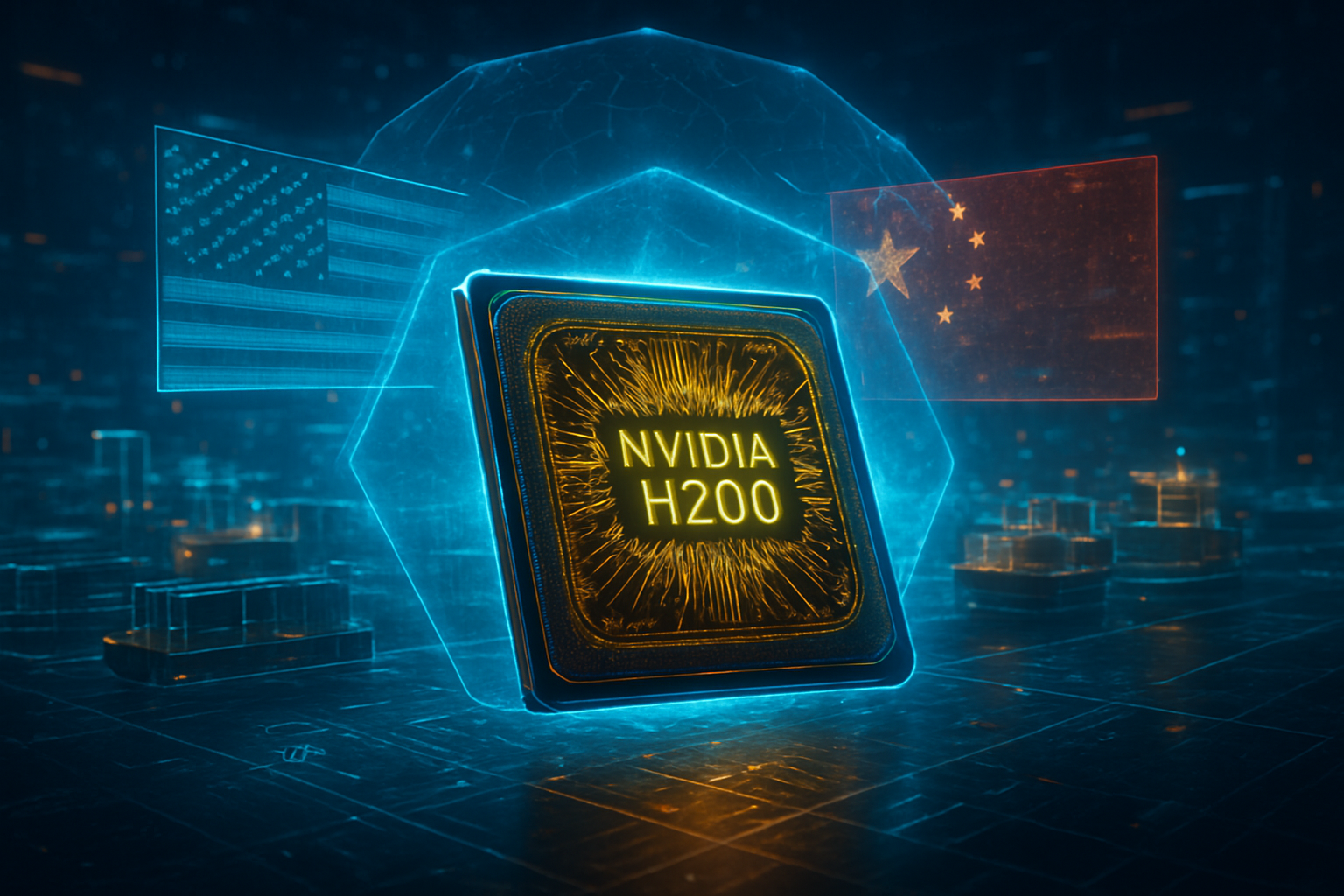
The shift to glass substrates is necessitated by the physical limitations of Ajinomoto Build-up Film (ABF) and Bismaleimide Triazine (BT) resins, which have been the standard for chip packaging since the 1990s. As AI chips like NVIDIA's (NASDAQ: NVDA) Blackwell successors and domestic Chinese alternatives push toward larger die sizes and higher power consumption, organic substrates suffer from significant "warpage"—the bending of the material under heat. Glass, however, offers a Coefficient of Thermal Expansion (CTE) that closely matches silicon (3-5 ppm/°C compared to organic’s 12-17 ppm/°C). This thermal stability ensures that as chips heat up, the substrate and the silicon expand at the same rate, preventing cracks and ensuring the integrity of the tens of thousands of micro-bumps connecting the chiplets.
Beyond thermal stability, glass substrates provide a revolutionary leap in interconnect density. Through the use of Through-Glass Via (TGV) technology—a laser-drilling process that creates microscopic vertical paths through the glass—manufacturers can achieve ten times the via density of organic materials. This allows for significantly shorter signal paths between the GPU and High Bandwidth Memory (HBM), which is critical for reducing latency and power consumption in AI workloads. Furthermore, glass is inherently flatter than organic materials, allowing for more precise lithography at the "panel level." In early 2026, Chinese manufacturers have demonstrated the ability to produce 515mm x 510mm glass panels, offering a throughput far exceeding traditional wafer-level packaging and slashing the cost of high-performance AI hardware.
Technical experts in the packaging community have noted that China’s approach uniquely blends its dominance in flat-panel display (FPD) technology with semiconductor manufacturing. While global giants like Intel (NASDAQ: INTC) and Samsung Electronics (KRX: 005930) have been researching glass substrates for years, China’s ability to repurpose existing LCD and OLED production lines for semiconductor glass has given it an unexpected speed advantage. The ability to use standardized, large-format glass allows for a "panel-level" economy of scale that traditional semiconductor firms are only now beginning to replicate.
Market Disruption: A New Competitive Frontier
The industrial landscape for glass substrates is rapidly consolidating around several key Chinese players who are now competing directly with Western and South Korean giants. JCET Group (SSE: 600584), China’s largest Outsourced Semiconductor Assembly and Test (OSAT) provider, announced in late 2025 that it had successfully integrated glass core substrates into its 1.6T optical module and Co-Packaged Optics (CPO) solutions. This development places JCET in direct competition with Taiwan Semiconductor Manufacturing Company (NYSE: TSM) and its CoWoS (Chip on Wafer on Substrate) technology, offering a glass-based alternative that promises better signal integrity for high-speed data center networking.
The move has also seen the entry of display giants into the semiconductor arena. BOE Technology Group (SZSE: 000725), the world’s largest LCD manufacturer, has pivoted significant R&D resources toward its semiconductor glass division. By Jan 2026, BOE has already transitioned from 8-inch pilot lines to full-scale panel production, leveraging its expertise in ultra-thin glass to produce substrates with "ultra-low warpage." Similarly, Visionox (SZSE: 002387) recently committed 5 billion yuan (approximately $700 million) to accelerate its glass substrate commercialization, targeting the high-end smartphone and AIoT sectors where power efficiency is paramount.
For the global market, this represents a significant threat to the dominance of established players like Intel and Samsung, who have also identified glass as the future of packaging. While Intel has touted its glass substrate roadmap for the 2026-2030 window, the sheer volume of investment and state coordination within China could allow domestic firms to capture the mid-market and high-growth segments of the AI hardware industry first. Companies specializing in laser equipment, such as Han's Laser (SZSE: 002008), are also benefiting from this shift, as the demand for high-precision TGV drilling equipment skyrockets, creating a self-sustaining domestic ecosystem that is increasingly decoupled from Western toolmakers.
Geopolitical Implications and Global Strategy
The strategic pivot to glass substrates is a cornerstone of China's broader push for "semiconductor sovereignty." As access to the most advanced extreme ultraviolet (EUV) lithography tools remains restricted, the Chinese government has identified "advanced packaging" as a viable "Plan B" to keep pace with global AI developments. By stacking multiple less-advanced chips on a high-performance glass substrate, China can create powerful "chiplet" systems that rival the performance of monolithic chips produced on more advanced nodes. This strategy effectively moves the battleground from front-end fabrication to back-end assembly, where China already holds a significant global market share.
The 15th Five-Year Plan (2026-2030) reportedly highlights advanced packaging materials, specifically TGV and glass core technologies, as national priorities. The government’s "Big Fund" Phase III has funneled billions into the Suzhou and Wuxi industrial clusters, creating a "Glass Substrate Valley" that mimics the success of the Silicon Valley or the Hsinchu Science Park. This state-backed coordination ensures that raw material suppliers, equipment makers, and packaging houses are vertically integrated, reducing the risk of supply chain disruptions that have plagued the organic substrate market in recent years.
However, this shift also raises concerns about further fragmentation of the global semiconductor supply chain. As China builds a proprietary ecosystem around specific glass formats and TGV standards, it creates a "standardization wall" that could make it difficult for international firms to integrate Chinese-made components into Western-designed systems. The competition is no longer just about who can make the smallest transistor, but who can build the most efficient "system-in-package" (SiP). In this regard, the glass substrate is the "new oil" of the AI hardware era, and China’s early lead in mass production could give it significant leverage over the global AI infrastructure.
The Horizon: 2026 and Beyond
Looking ahead, the next 24 months will be critical for the maturation of glass substrate technology. We expect to see the first wave of commercially available AI accelerators utilizing glass cores hit the market by mid-2026, with JCET and BOE likely being the first to announce high-volume partnerships with domestic AI chip designers like Biren Technology and Moore Threads. These applications will likely focus on high-performance computing (HPC) and data center chips first, before trickling down to consumer devices such as laptops and smartphones that require intensive AI processing at the edge.
One of the primary challenges remaining is the refinement of the TGV process for mass production. While laser drilling is precise, achieving 100% yield across a large 515mm panel remains a high bar. Furthermore, the industry must develop new inspection and testing protocols for glass, as the material behaves differently than resin under mechanical stress. Predictions from industry analysts suggest that by 2028, glass substrates could account for over 30% of the high-end packaging market, eventually displacing organic substrates entirely for any chip with a power draw exceeding 300 watts.
As the industry moves toward 3D-integrated circuits where memory and logic are stacked vertically, the role of glass will only become more central. The potential for glass to act not just as a carrier, but as an active component—incorporating integrated photonics and optical waveguides directly into the substrate—is already being explored in Chinese research institutes. If successful, this would represent the most significant leap in semiconductor packaging since the invention of the flip-chip.
A New Era in Semiconductor Packaging
In summary, China’s aggressive move into glass substrates represents a major strategic gambit that could redefine the global AI supply chain. By aligning its industrial policy with the physical requirements of future AI chips, Beijing has found a way to leverage its massive manufacturing base in display glass to solve one of the most pressing bottlenecks in high-performance computing. The combination of state-backed funding, a coordinated industry alliance, and a "panel-level" production approach gives Chinese firms a formidable edge in the race for packaging dominance.
This development is likely to be remembered as a turning point in semiconductor history—the moment when the focus of innovation shifted from the transistor itself to the environment that surrounds and connects it. For the global tech industry, the message is clear: the next generation of AI power will not just be built on silicon, but on glass. In the coming months, the industry should watch closely for the first yield reports from JCET’s mass production lines and the official rollout of BOE’s semiconductor-grade glass panels, as these will be the true indicators of how quickly the "post-organic" future will arrive.
This content is intended for informational purposes only and represents analysis of current AI developments.
TokenRing AI delivers enterprise-grade solutions for multi-agent AI workflow orchestration, AI-powered development tools, and seamless remote collaboration platforms.
For more information, visit https://www.tokenring.ai/.