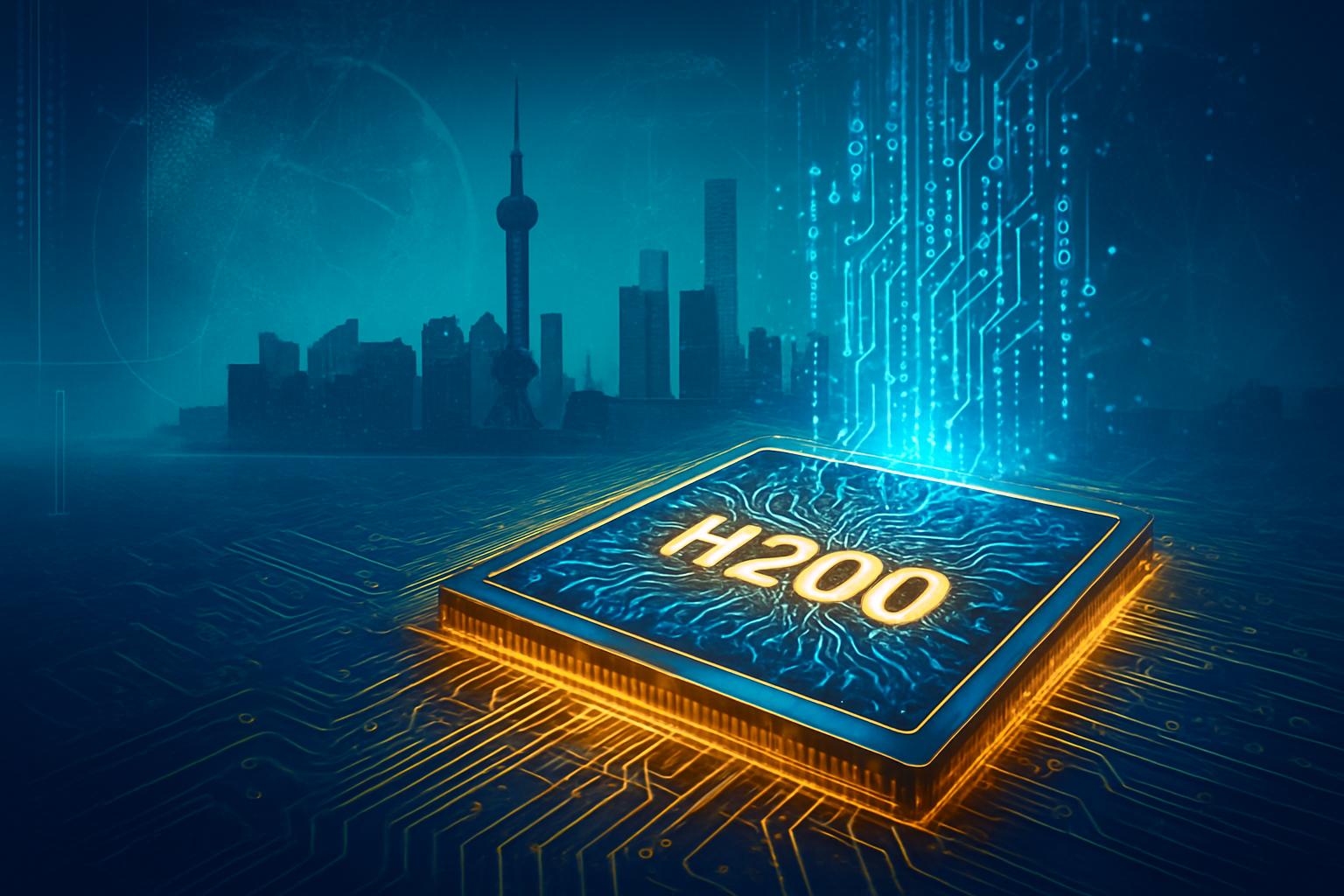
As of late January 2026, the global semiconductor industry has entered a volatile new chapter. Following years of tightening export controls, a complex "revenue-for-access" truce has emerged between Washington and Beijing, fundamentally altering the strategic calculus for NVIDIA Corporation (NASDAQ: NVDA). While recent regulatory shifts have nominally reopened the door for NVIDIA’s high-performance H200 chips, the landscape they return to is no longer a monopoly. China’s major technology conglomerates—once NVIDIA’s most reliable customers—are increasingly rejecting "downgraded" western silicon in favor of domestic self-sufficiency.
This pivot represents a watershed moment in the AI arms race. The rejection of NVIDIA’s previous "China-specific" offerings, such as the H20, has forced a recalibration of the entire regional revenue strategy for the Santa Clara-based giant. As Chinese firms like Alibaba Group Holding Ltd. (NYSE: BABA) and Tencent Holdings Ltd. (HKG: 0700) accelerate their transition to homegrown architectures, the global AI supply chain is bifurcating into two distinct, and increasingly incompatible, ecosystems.
The technical catalyst for this shift lies in the stark performance gap of previous "compliant" chips. Throughout 2025, NVIDIA attempted to navigate U.S. Department of Commerce restrictions by offering the H20, a modified version of its Hopper architecture with significantly throttled processing power. Research indicates the H20 delivered roughly 40% of the compute density of the flagship H100, a deficit that rendered it nearly useless for training the next generation of frontier Large Language Models (LLMs). This performance "floor" became a breaking point; by late 2025, Chinese cloud providers began canceling massive H20 orders, citing an inability to remain competitive with Western AI labs using unencumbered hardware.
In response, the market has seen the rise of legitimate domestic rivals, most notably Huawei’s Ascend 910C. As of January 2026, the 910C has become the benchmark for Chinese AI compute, offering system-level innovations such as the CloudMatrix 384—a clustered architecture designed to rival NVIDIA’s high-bandwidth interconnects. While the individual H200 chip still maintains a roughly 32% processing advantage over the 910C, Huawei has narrowed the gap significantly in memory bandwidth and vertical software integration via its CANN (Compute Architecture for Neural Networks) framework. This progress has empowered Chinese firms to take a "dual-track" approach: utilizing NVIDIA's H200 for the most intensive training phases while shifting the bulk of their inference and mid-tier training to domestic hardware.
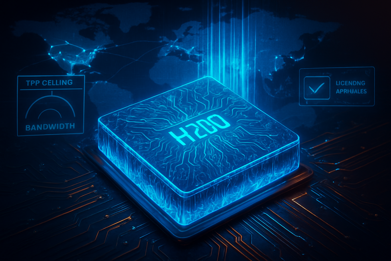
The competitive implications of this shift are profound for the world's leading chipmakers. For NVIDIA, the China market—which historically accounted for up to 25% of total revenue—plummeted to mid-single digits in late 2025 before the recent "case-by-case" review policy for the H200 was enacted on January 15, 2026. While analysts project this opening could unlock a $40 billion to $50 billion annual opportunity, it comes with a heavy "geopolitical tax." Under the new "Trump-Huang Revenue Model," a 25% value-based tariff is now imposed on every advanced AI chip exported to China, with proceeds directed to the U.S. Treasury. This policy creates an unprecedented scenario where NVIDIA must manage record-high demand while facing significant pressure on net profit margins.
Beyond NVIDIA, the ripples are felt by Advanced Micro Devices, Inc. (NASDAQ: AMD) and Intel Corporation (NASDAQ: INTC), both of whom are struggling to secure similar "green light" status for their high-end accelerators like the MI325X. Meanwhile, the biggest beneficiaries of this tension are domestic Chinese semiconductor players. Semiconductor Manufacturing International Corporation (SHA: 601238), or SMIC, has seen a surge in orders as it refines its 7nm and 5nm-class processes to support Huawei’s ramping production. The emergence of Alibaba’s internal chip unit, T-Head, and its Zhenwu 810E processor, further illustrates how tech giants are pivoting from being NVIDIA’s customers to becoming its primary regional competitors.
On a broader scale, this development signals the official end of a unified global AI stack. The "50% domestic equipment rule" reportedly implemented by Chinese regulators in late 2025 mandates that state-funded and even some private data centers must source half of their hardware locally. This policy serves as a protective barrier, ensuring that even as NVIDIA regains access to the market, domestic players like Huawei and Cambricon Technologies (SHA: 688256) are guaranteed a significant market share. This is AI sovereignty in action—a direct response to years of U.S. sanctions that have convinced Beijing that reliance on Western silicon is a terminal risk.
The geopolitical landscape of 2026 is now defined by what experts call the "Silicon Splinternet." The U.S. strategy has shifted from a total blockade to a tactical "locking in" effect. By allowing the H200 back into the market under heavy tariffs, the U.S. aims to keep Chinese developers tethered to NVIDIA’s CUDA software ecosystem, preventing a total migration to Huawei’s alternative frameworks. This is a delicate balancing act; too much restriction accelerates Chinese innovation, while too little allows China to reach parity with Western AI capabilities. The current status quo is a high-stakes compromise where innovation is effectively taxed to fund national security.
Looking ahead, the next twelve to eighteen months will be defined by the race to the "post-Hopper" era. NVIDIA is already preparing its Blackwell-based (B20/B30A) offerings for the Chinese market, which will likely face even stricter scrutiny and higher tariffs. Simultaneously, the focus is shifting to the upcoming "Rubin" architecture, slated for late 2026. Experts predict that the battleground will move from raw compute power to the "interconnect war," as Chinese firms attempt to replicate NVIDIA’s NVLink technology to overcome the limitations of individual chip performance through massive, efficient clusters.
However, significant hurdles remain for China's domestic ambitions. Yield rates at SMIC and the ongoing struggle to secure advanced Lithography equipment continue to plague the mass production of the Ascend 910C and 910D. Furthermore, the transition from CUDA to domestic software stacks remains a "painful and buggy" process for developers, as evidenced by the technical setbacks faced by AI startup DeepSeek during its recent training cycles. The coming months will determine if the current "dual-track" strategy is a temporary bridge or a permanent divorce from the Western supply chain.
The "Silicon Standoff" of 2026 marks a definitive turning point in the history of the semiconductor industry. NVIDIA remains the undisputed king of performance, but its crown is being increasingly weighed down by the heavy machinery of international diplomacy. The rejection of the H20 and the cautious, tariff-laden adoption of the H200 demonstrate that in the modern era, a chip’s technical specifications are only as valuable as the geopolitical permissions attached to them.
As we move deeper into 2026, the industry must watch two critical indicators: the success of Huawei’s next-gen 910D production and the sustainability of the 25% "AI tariff" model. If Chinese firms can successfully migrate their LLM training to domestic hardware without a significant loss in intelligence, the "NVIDIA era" in the East may be nearing its conclusion. For now, the world remains in a state of watchful tension, where every transistor shipped across the Pacific is a move in a global game of chess.
This content is intended for informational purposes only and represents analysis of current AI developments.
TokenRing AI delivers enterprise-grade solutions for multi-agent AI workflow orchestration, AI-powered development tools, and seamless remote collaboration platforms.
For more information, visit https://www.tokenring.ai/.