The relentless march of technological progress, particularly in artificial intelligence (AI), 5G/6G communication, electric vehicles, and the burgeoning Internet of Things (IoT), is pushing the very limits of traditional silicon-based electronics. As Moore's Law, which has guided the semiconductor industry for decades, begins to falter, a quiet yet profound revolution in materials science is taking center stage. New materials, with their extraordinary electrical, thermal, and mechanical properties, are not merely incremental improvements; they are fundamentally redefining what's possible in chip design, promising a future of faster, smaller, more energy-efficient, and functionally diverse electronic devices. This shift is critical for sustaining the pace of innovation, addressing the escalating demands of modern computing, and overcoming the inherent physical and economic constraints that silicon now presents.
The immediate significance of this materials science revolution is multifaceted. It promises continued miniaturization and unprecedented performance enhancements, enabling denser and more powerful chips than ever before. Critically, many of these novel materials inherently consume less power and generate less heat, directly addressing the critical need for extended battery life in mobile devices and substantial energy reductions in vast data centers. Beyond traditional computing metrics, these materials are unlocking entirely new functionalities, from flexible electronics and advanced sensors to neuromorphic computing architectures and robust high-frequency communication systems, laying the groundwork for the next generation of intelligent technologies.
The Atomic Edge: Unpacking the Technical Revolution in Chip Materials
The core of this revolution lies in the unique properties of several advanced materials that are poised to surpass silicon in specific applications. These innovations are directly tackling silicon's limitations, such as quantum tunneling, increased leakage currents, and difficulties in maintaining gate control at sub-5nm scales.
Wide Bandgap (WBG) Semiconductors, notably Gallium Nitride (GaN) and Silicon Carbide (SiC), stand out for their superior electrical efficiency, heat resistance, higher breakdown voltages, and improved thermal stability. GaN, with its high electron mobility, is proving indispensable for fast switching in telecommunications, radar systems, 5G base stations, and rapid-charging technologies. SiC excels in high-power applications for electric vehicles, renewable energy systems, and industrial machinery due to its robust performance at elevated voltages and temperatures, offering significantly reduced energy losses compared to silicon.
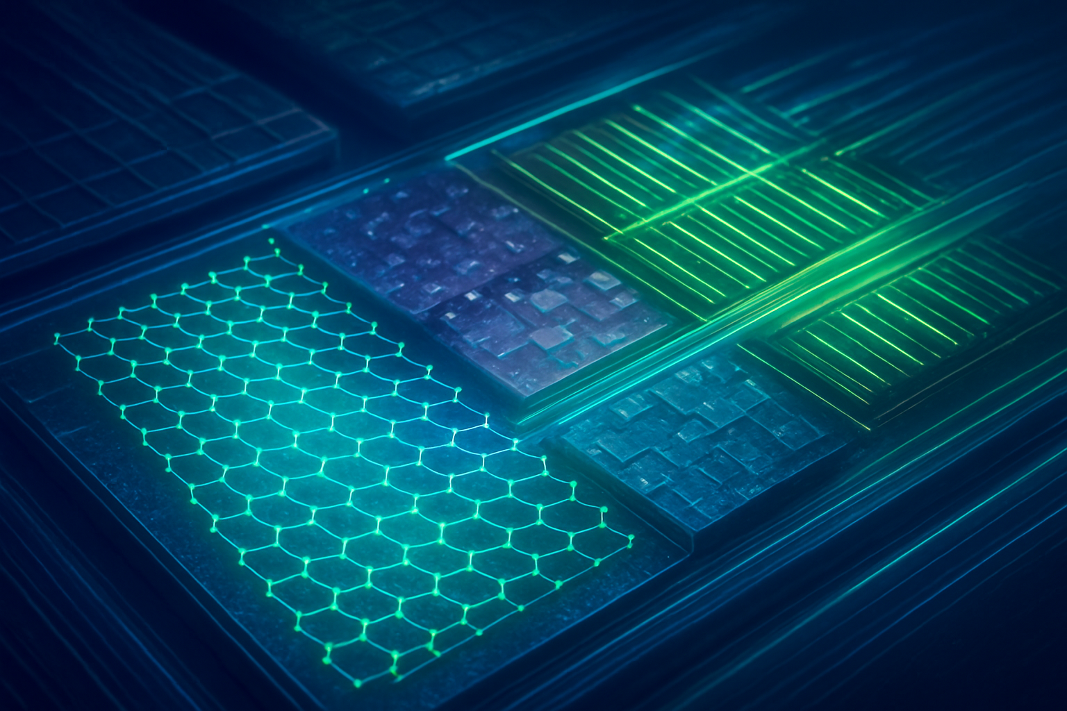
Two-Dimensional (2D) Materials represent a paradigm shift in miniaturization. Graphene, a single layer of carbon atoms, boasts exceptional electrical conductivity, strength, and ultra-high electron mobility, allowing for electricity conduction at higher speeds with minimal heat generation. This makes it a strong candidate for ultra-high-speed transistors, flexible electronics, and advanced sensors. Other 2D materials like Transition Metal Dichalcogenides (TMDs) such as molybdenum disulfide, and hexagonal boron nitride, enable atomic-thin channel transistors and monolithic 3D integration. Their tunable bandgaps and high thermal conductivity make them suitable for next-generation transistors, flexible displays, and even foundational elements for quantum computing. These materials allow for device scaling far beyond silicon's physical limits, addressing the fundamental challenges of miniaturization.
Ferroelectric Materials are introducing a new era of memory and logic. These materials are non-volatile, operate at low power, and offer fast switching capabilities with high endurance. Their integration into Ferroelectric Random Access Memory (FeRAM) and Ferroelectric Field-Effect Transistors (FeFETs) provides energy-efficient memory and logic devices crucial for AI chips and neuromorphic computing, which demand efficient data storage and processing close to the compute units.
Furthermore, III-V Semiconductors like Gallium Arsenide (GaAs) and Indium Phosphide (InP) are vital for optoelectronics and high-frequency applications. Unlike silicon, their direct bandgap allows for efficient light emission and absorption, making them excellent for LEDs, lasers, photodetectors, and high-speed RF devices. Spintronic Materials, which utilize the spin of electrons rather than their charge, promise non-volatile, lower power, and faster data processing. Recent breakthroughs in materials like iron palladium are enabling spintronic devices to shrink to unprecedented sizes. Emerging contenders like Cubic Boron Arsenide are showing superior heat and electrical conductivity compared to silicon, while Indium-based materials are being developed to facilitate extreme ultraviolet (EUV) patterning for creating incredibly precise 3D circuits.
These materials differ fundamentally from silicon by overcoming its inherent performance bottlenecks, thermal constraints, and energy efficiency limits. They offer significantly higher electron mobility, better thermal dissipation, and lower power operation, directly addressing the challenges that have begun to impede silicon's continued progress. The initial reaction from the AI research community and industry experts is one of cautious optimism, recognizing the immense potential while also acknowledging the significant manufacturing and integration challenges that lie ahead. The consensus is that a hybrid approach, combining silicon with these advanced materials, will likely define the next decade of chip innovation.
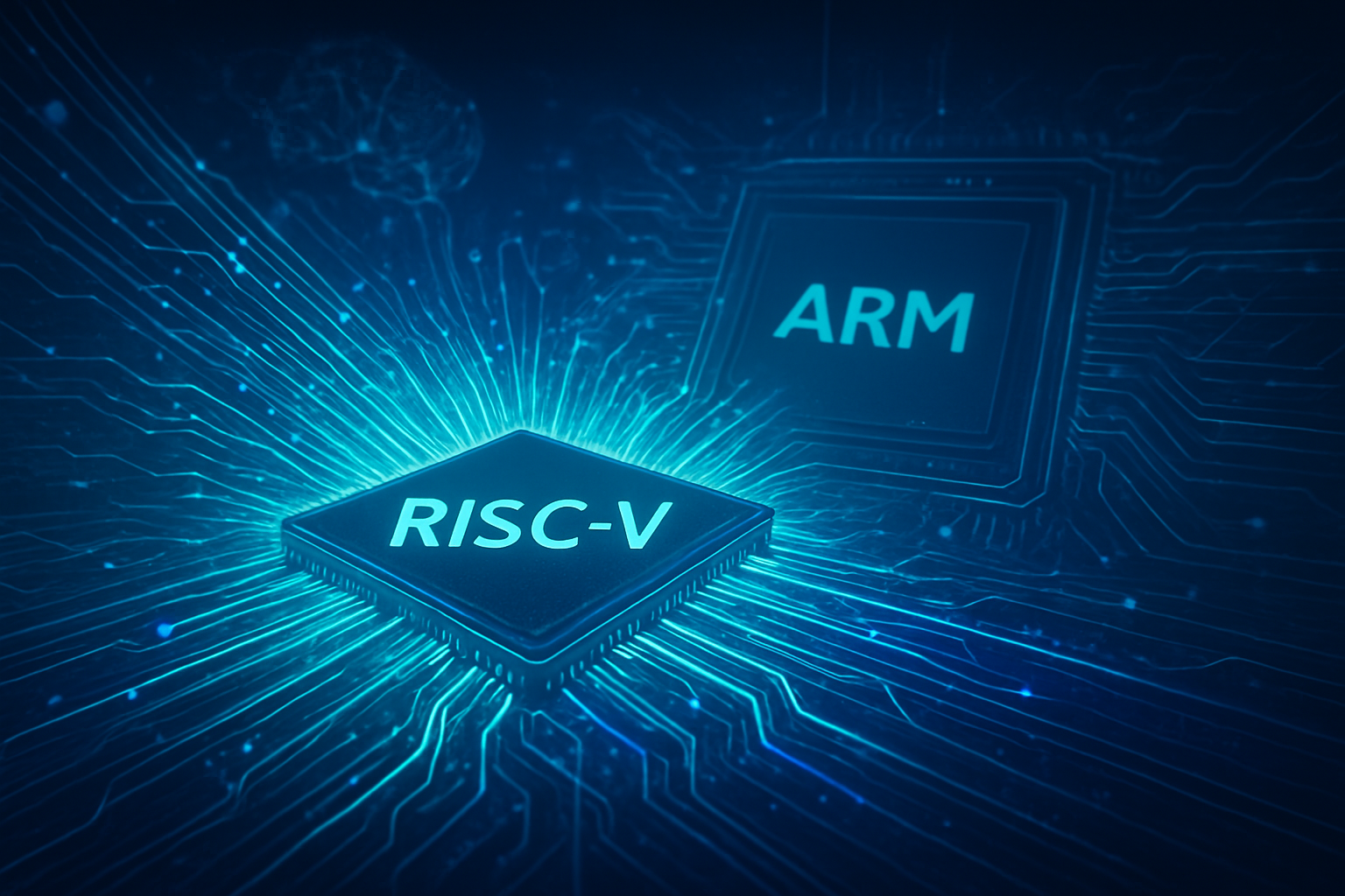
Corporate Chessboard: The Impact on Tech Giants and Startups
The materials science revolution in chip design is poised to redraw the competitive landscape for AI companies, tech giants, and startups alike. Companies deeply invested in semiconductor manufacturing, advanced materials research, and specialized computing stand to benefit immensely, while others may face significant disruption if they fail to adapt.
Intel (NASDAQ: INTC), a titan in the semiconductor industry, is heavily investing in new materials research and advanced packaging techniques to maintain its competitive edge. Their focus includes integrating novel materials into future process nodes and exploring hybrid bonding technologies to stack different materials and functionalities. Similarly, Taiwan Semiconductor Manufacturing Company (TSMC) (NYSE: TSM), the world's largest dedicated independent semiconductor foundry, is at the forefront of adopting new materials and processes to enable their customers to design cutting-edge chips. Their ability to integrate these advanced materials into high-volume manufacturing will be crucial for the industry. Samsung (KRX: 005930), another major player in both memory and logic, is also actively exploring ferroelectrics, 2D materials, and advanced packaging to enhance its product portfolio, particularly for AI accelerators and mobile processors.
The competitive implications for major AI labs and tech companies are profound. Companies like NVIDIA (NASDAQ: NVDA), which dominates the AI accelerator market, will benefit from the ability to design even more powerful and energy-efficient GPUs and custom AI chips by leveraging these new materials. Faster transistors, more efficient memory, and better thermal management directly translate to higher AI training and inference speeds. Tech giants like Google (NASDAQ: GOOGL), Amazon (NASDAQ: AMZN), and Microsoft (NASDAQ: MSFT), all heavily reliant on data centers and custom AI silicon, will gain strategic advantages through improved performance-per-watt ratios, leading to reduced operational costs and enhanced service capabilities.
Startups focused on specific material innovations or novel chip architectures based on these materials are also poised for significant growth. Companies developing GaN or SiC power semiconductors, 2D material fabrication techniques, or spintronic memory solutions could become acquisition targets or key suppliers to the larger players. The potential disruption to existing products is considerable; for instance, traditional silicon-based power electronics may gradually be supplanted by more efficient GaN and SiC alternatives. Memory technologies could see a shift towards ferroelectric RAM (FeRAM) or spintronic memory, offering superior speed and non-volatility. Market positioning will increasingly depend on a company's ability to innovate with these materials, secure supply chains, and effectively integrate them into commercially viable products. Strategic advantages will accrue to those who can master the complex manufacturing processes and design methodologies required for these next-generation chips.
A New Era of Computing: Wider Significance and Societal Impact
The materials science revolution in chip design represents more than just an incremental step; it signifies a fundamental shift in how we approach computing and its potential applications. This development fits perfectly into the broader AI landscape and trends, particularly the increasing demand for specialized hardware that can handle the immense computational and data-intensive requirements of modern AI models, from large language models to complex neural networks.
The impacts are far-reaching. On a technological level, these new materials enable the continuation of miniaturization and performance scaling, ensuring that the exponential growth in computing power can persist, albeit through different means than simply shrinking silicon transistors. This will accelerate advancements in all fields touched by AI, including healthcare (e.g., faster drug discovery, more accurate diagnostics), autonomous systems (e.g., more reliable self-driving cars, advanced robotics), and scientific research (e.g., complex simulations, climate modeling). Energy efficiency improvements, driven by materials like GaN and SiC, will have a significant environmental impact, reducing the carbon footprint of data centers and electronic devices.
However, potential concerns also exist. The complexity of manufacturing and integrating these novel materials could lead to higher initial costs and slower adoption rates in some sectors. There are also significant challenges in scaling production to meet global demand, and the supply chain for some exotic materials may be less robust than that for silicon. Furthermore, the specialized knowledge required to work with these materials could create a talent gap in the industry.
Comparing this to previous AI milestones and breakthroughs, this materials revolution is akin to the invention of the transistor itself or the shift from vacuum tubes to solid-state electronics. While not a direct AI algorithm breakthrough, it is an foundational enabler that will unlock the next generation of AI capabilities. Just as improved silicon technology fueled the deep learning revolution, these new materials will provide the hardware bedrock for future AI paradigms, including neuromorphic computing, in-memory computing, and potentially even quantum AI. It signifies a move beyond the silicon monoculture, embracing a diverse palette of materials to optimize specific functions, leading to heterogeneous computing architectures that are far more efficient and powerful than anything possible with silicon alone.
The Horizon: Future Developments and Expert Predictions
The trajectory of materials science in chip design points towards exciting near-term and long-term developments, promising a future where electronics are not only more powerful but also more integrated and adaptive. Experts predict a continued move towards heterogeneous integration, where different materials and components are optimally combined on a single chip or within advanced packaging. This means silicon will likely coexist with GaN, 2D materials, ferroelectrics, and other specialized materials, each performing the tasks it's best suited for.
In the near term, we can expect to see wider adoption of GaN and SiC in power electronics and 5G infrastructure, driving efficiency gains in everyday devices and networks. Research into 2D materials will likely yield commercial applications in ultra-thin, flexible displays and high-performance sensors within the next few years. Ferroelectric memories are also on the cusp of broader integration into AI accelerators, offering low-power, non-volatile memory solutions essential for edge AI devices.
Longer term, the focus will shift towards more radical transformations. Neuromorphic computing, which mimics the structure and function of the human brain, stands to benefit immensely from materials that can enable highly efficient synaptic devices and artificial neurons, such as phase-change materials and advanced ferroelectrics. The integration of spintronic devices could lead to entirely new classes of ultra-low-power, non-volatile logic and memory. Furthermore, breakthroughs in quantum materials could pave the way for practical quantum computing, moving beyond current experimental stages.
Potential applications on the horizon include truly flexible and wearable AI devices, energy-harvesting chips that require minimal external power, and AI systems capable of learning and adapting with unprecedented efficiency. Challenges that need to be addressed include developing cost-effective and scalable manufacturing processes for these novel materials, ensuring their long-term reliability and stability, and overcoming the complex integration hurdles of combining disparate material systems. Experts predict that the next decade will be characterized by intense interdisciplinary collaboration between materials scientists, device physicists, and computer architects, driving a new era of innovation where the boundaries of hardware and software blur, ultimately leading to an explosion of new capabilities in artificial intelligence and beyond.
Wrapping Up: A New Foundation for AI's Future
The materials science revolution currently underway in chip design is far more than a technical footnote; it is a foundational shift that will underpin the next wave of advancements in artificial intelligence and electronics as a whole. The key takeaways are clear: traditional silicon is reaching its physical limits, and a diverse array of new materials – from wide bandgap semiconductors like GaN and SiC, to atomic-thin 2D materials, efficient ferroelectrics, and advanced spintronic compounds – are stepping in to fill the void. These materials promise not only continued miniaturization and performance scaling but also unprecedented energy efficiency and novel functionalities that were previously unattainable.
This development's significance in AI history cannot be overstated. Just as the invention of the transistor enabled the first computers, and the refinement of silicon manufacturing powered the internet and smartphone eras, this materials revolution will provide the hardware bedrock for the next generation of AI. It will facilitate the creation of more powerful, efficient, and specialized AI accelerators, enabling breakthroughs in everything from autonomous systems to personalized medicine. The shift towards heterogeneous integration, where different materials are optimized for specific tasks, will redefine chip architecture and unlock new possibilities for in-memory and neuromorphic computing.
In the coming weeks and months, watch for continued announcements from major semiconductor companies and research institutions regarding new material breakthroughs and integration techniques. Pay close attention to developments in extreme ultraviolet (EUV) lithography for advanced patterning, as well as progress in 3D stacking and hybrid bonding technologies that will enable the seamless integration of these diverse materials. The future of AI is intrinsically linked to the materials that power it, and the current revolution promises a future far more dynamic and capable than we can currently imagine.
This content is intended for informational purposes only and represents analysis of current AI developments.
TokenRing AI delivers enterprise-grade solutions for multi-agent AI workflow orchestration, AI-powered development tools, and seamless remote collaboration platforms.
For more information, visit https://www.tokenring.ai/.