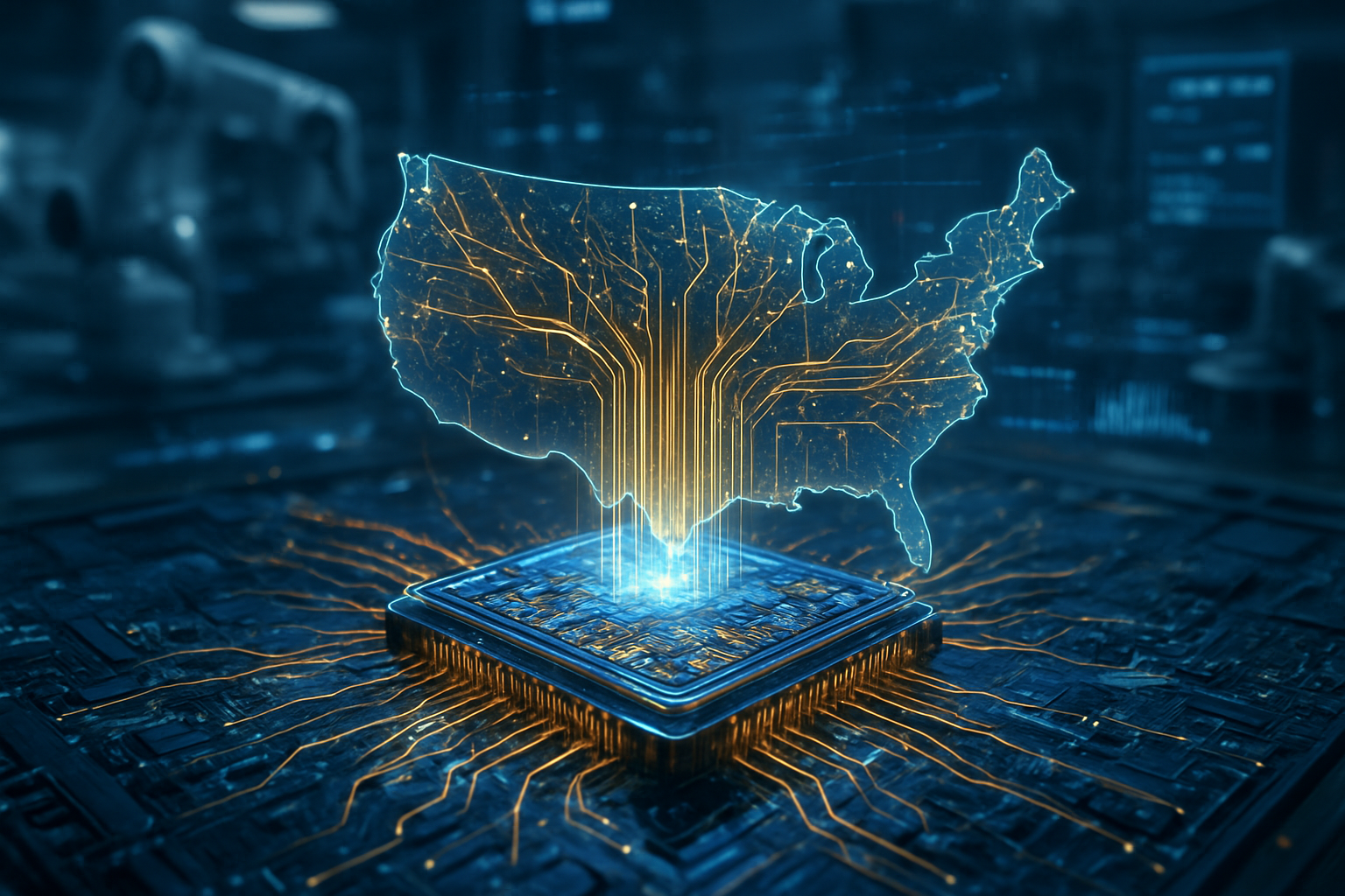
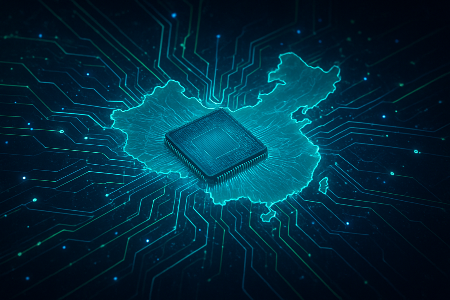
Tag: Chip Manufacturing

  • Global Chip Renaissance: Trillions Poured into Next-Gen Semiconductor Fabs

    Global Chip Renaissance: Trillions Poured into Next-Gen Semiconductor Fabs

    The world is witnessing an unprecedented surge in investment within the semiconductor manufacturing sector, a monumental effort to reshape the global supply chain and meet the insatiable demand for advanced chips. With approximately $1 trillion earmarked for new fabrication plants (fabs) through 2030, and 97 new high-volume fabs expected to be operational between 2023 and 2025, the industry is undergoing a profound transformation. This massive capital injection, driven by geopolitical imperatives, a quest for supply chain resilience, and the explosive growth of Artificial Intelligence (AI), promises to fundamentally alter where and how the world's most critical components are produced.

    This global chip renaissance is particularly evident in the United States, where initiatives like the CHIPS and Science Act are catalyzing significant domestic expansion. Major players such as Taiwan Semiconductor Manufacturing Company (TSMC) (NYSE: TSM), Intel (NASDAQ: INTC), and Samsung (KRX: 005930) are committing tens of billions of dollars to construct state-of-the-art facilities, not only in the U.S. but also in Europe and Asia. These investments are not merely about increasing capacity; they represent a strategic pivot towards diversifying manufacturing hubs, fostering innovation in leading-edge process technologies, and securing the foundational elements for the next wave of technological advancement.

    A Deep Dive into the Fab Frenzy: Technical Specifications and Industry Reactions

    The scale and technical ambition of these new fab projects are staggering. TSMC, for instance, is expanding its U.S. investment to an astonishing $165 billion, encompassing three new advanced fabs, two advanced packaging facilities, and a major R&D center in Phoenix, Arizona. The first of these Arizona fabs, already in production since late 2024, is reportedly supplying Apple (NASDAQ: AAPL) with cutting-edge chips. Beyond the U.S., TSMC is also bolstering its presence in Japan and Europe through strategic joint ventures.

    Intel (NASDAQ: INTC) is equally aggressive, pledging over $100 billion in the U.S. across Arizona, New Mexico, Oregon, and Ohio. Its newest Arizona plant, Fab 52, is already utilizing Intel's advanced 18A process technology (a 2-nanometer-class node), demonstrating a commitment to leading-edge manufacturing. In Ohio, two new fabs are slated to begin production by 2025, while its New Mexico facility, Fab 9, opened in January 2024, focuses on advanced packaging. Globally, Intel is investing €17 billion in a new fab in Magdeburg, Germany, and upgrading its Irish plant for EUV lithography. These moves signify a concerted effort by Intel to reclaim its manufacturing leadership and compete directly with TSMC and Samsung at the most advanced nodes.

    Samsung Foundry (KRX: 005930) is expanding its Taylor, Texas, fab complex to approximately $44 billion, which includes an initial $17 billion production facility, an additional fab module, an advanced packaging facility, and an R&D center. The first Taylor fab is expected to be completed by the end of October 2025. This facility is designed to produce advanced logic chips for critical applications in mobile, 5G, high-performance computing (HPC), and artificial intelligence. Initial reactions from the AI research community and industry experts are overwhelmingly positive, recognizing these investments as crucial for fueling the next generation of AI hardware, which demands ever-increasing computational power and efficiency. The shift towards 2nm-class nodes and advanced packaging is seen as a necessary evolution to keep pace with AI's exponential growth.

    Reshaping the AI Landscape: Competitive Implications and Market Disruption

    These massive investments in semiconductor manufacturing facilities will profoundly reshape the competitive landscape for AI companies, tech giants, and startups alike. Companies that stand to benefit most are those at the forefront of AI development, such as NVIDIA (NASDAQ: NVDA), which relies heavily on advanced chips for its GPUs, and major cloud providers like Amazon (NASDAQ: AMZN), Google (NASDAQ: GOOGL), and Microsoft (NASDAQ: MSFT) that power AI workloads. The increased domestic and diversified production capacity will offer greater supply security and potentially reduce lead times for these critical components.

    The competitive implications for major AI labs and tech companies are significant. With more advanced fabs coming online, particularly those capable of producing cutting-edge 2nm-class chips and advanced packaging, the race for AI supremacy will intensify. Companies with early access or strong partnerships with these new fabs will gain a strategic advantage in developing and deploying more powerful and efficient AI models. This could disrupt existing products or services that are currently constrained by chip availability or older manufacturing processes, paving the way for a new generation of AI hardware and software innovations.

    Furthermore, the focus on leading-edge technologies and advanced packaging will foster an environment ripe for innovation among AI startups. Access to more sophisticated and specialized chips will enable smaller companies to develop niche AI applications that were previously unfeasible due to hardware limitations. This market positioning and strategic advantage will not only benefit the chipmakers themselves but also create a ripple effect throughout the entire AI ecosystem, driving further advancements and accelerating the pace of AI adoption across various industries.

    Wider Significance: Broadening the AI Horizon and Addressing Concerns

    The monumental investments in semiconductor fabs fit squarely within the broader AI landscape, addressing critical needs for the technology's continued expansion. The sheer demand for computational power required by increasingly complex AI models, from large language models to advanced machine learning algorithms, necessitates a robust and resilient chip manufacturing infrastructure. These new fabs, with their focus on leading-edge logic and advanced memory like High Bandwidth Memory (HBM), are the foundational pillars upon which the next era of AI innovation will be built.

    The impacts of these investments extend beyond mere capacity. They represent a strategic geopolitical realignment, aimed at reducing reliance on single points of failure in the global supply chain, particularly in light of recent geopolitical tensions. The CHIPS and Science Act in the U.S. and similar initiatives in Europe and Japan underscore a collective understanding that semiconductor independence is paramount for national security and economic competitiveness. However, potential concerns linger, including the immense capital and operational costs, the increasing demand for raw materials, and persistent talent shortages. Some projects have already faced delays and cost overruns, highlighting the complexities of such large-scale endeavors.

    Comparing this to previous AI milestones, the current fab build-out can be seen as analogous to the infrastructure boom that enabled the internet's widespread adoption. Just as robust networking infrastructure was essential for the digital age, a resilient and advanced semiconductor manufacturing base is critical for the AI age. This wave of investment is not just about producing more chips; it's about producing better, more specialized chips that can unlock new frontiers in AI research and application, addressing the "hardware bottleneck" that has, at times, constrained AI's progress.

    The Road Ahead: Future Developments and Expert Predictions

    The coming years are expected to bring a continuous stream of developments stemming from these significant fab investments. In the near term, we will see more of the announced facilities, such as Samsung's Taylor, Texas, plant and Texas Instruments' (NASDAQ: TXN) Sherman facility, come online and ramp up production. This will lead to a gradual easing of supply chain pressures and potentially more competitive pricing for advanced chips. Long-term, experts predict a further decentralization of leading-edge semiconductor manufacturing, with the U.S., Europe, and Japan gaining significant shares of wafer fabrication capacity by 2032.

    Potential applications and use cases on the horizon are vast. With more powerful and efficient chips, we can expect breakthroughs in areas such as real-time AI processing at the edge, more sophisticated autonomous systems, advanced medical diagnostics powered by AI, and even more immersive virtual and augmented reality experiences. The increased availability of High Bandwidth Memory (HBM), for example, will be crucial for training and deploying even larger and more complex AI models.

    However, challenges remain. The industry will need to address the increasing demand for skilled labor, particularly engineers and technicians capable of operating and maintaining these highly complex facilities. Furthermore, the environmental impact of increased manufacturing, particularly in terms of energy consumption and waste, will require innovative solutions. Experts predict a continued focus on sustainable manufacturing practices and the development of even more energy-efficient chip architectures. The next big leaps in AI will undoubtedly be intertwined with the advancements made in these new fabs.

    A New Era of Chipmaking: Key Takeaways and Long-Term Impact

    The global surge in semiconductor manufacturing investments marks a pivotal moment in technological history, signaling a new era of chipmaking defined by resilience, innovation, and strategic diversification. The key takeaway is clear: the world is collectively investing trillions to ensure a robust and geographically dispersed supply of advanced semiconductors, recognizing their indispensable role in powering the AI revolution and virtually every other modern technology.

    This development's significance in AI history cannot be overstated. It represents a fundamental strengthening of the hardware foundation upon which all future AI advancements will be built. Without these cutting-edge fabs and the chips they produce, the ambitious goals of AI research and deployment would remain largely theoretical. The long-term impact will be a more secure, efficient, and innovative global technology ecosystem, less susceptible to localized disruptions and better equipped to handle the exponential demands of emerging technologies.

    In the coming weeks and months, we should watch for further announcements regarding production milestones from these new fabs, updates on government incentives and their effectiveness, and any shifts in the competitive dynamics between the major chipmakers. The successful execution of these massive projects will not only determine the future of AI but also shape global economic and geopolitical landscapes for decades to come.


    This content is intended for informational purposes only and represents analysis of current AI developments.

    TokenRing AI delivers enterprise-grade solutions for multi-agent AI workflow orchestration, AI-powered development tools, and seamless remote collaboration platforms.
    For more information, visit https://www.tokenring.ai/.

  • Forging a Resilient Future: Global Race to De-Risk the Semiconductor Supply Chain

    Forging a Resilient Future: Global Race to De-Risk the Semiconductor Supply Chain

    The global semiconductor industry, the bedrock of modern technology, is undergoing an unprecedented transformation driven by a concerted worldwide effort to build supply chain resilience. Spurred by geopolitical tensions, the stark lessons of the COVID-19 pandemic, and the escalating demand for chips across every sector, nations and corporations are investing trillions to diversify manufacturing, foster domestic capabilities, and secure a stable future for critical chip supplies. This pivot from a hyper-efficient, geographically concentrated model to one prioritizing redundancy and strategic independence marks a monumental shift with profound implications for global economics, national security, and technological innovation.

    The immediate significance of these initiatives is already palpable, manifesting in a massive surge of investments and a reshaping of the global manufacturing landscape. Governments, through landmark legislation like the U.S. CHIPS Act and the European Chips Act, are pouring billions into incentives for domestic production, while private sector investments are projected to reach trillions in the coming decade. This unprecedented financial commitment is catalyzing the establishment of new fabrication plants (fabs) in diverse regions, aiming to mitigate the vulnerabilities exposed by past disruptions and ensure the uninterrupted flow of the semiconductors that power everything from smartphones and AI data centers to advanced defense systems.

    A New Era of Strategic Manufacturing: Technical Deep Dive into Resilience Efforts

    The drive for semiconductor supply chain resilience is characterized by a multi-pronged technical and strategic approach, fundamentally altering how chips are designed, produced, and distributed. At its core, this involves a significant re-evaluation of the industry's historical reliance on just-in-time manufacturing and extreme geographical specialization, particularly in East Asia. The new paradigm emphasizes regionalization, technological diversification, and enhanced visibility across the entire value chain.

    A key technical advancement is the push for geographic diversification of advanced logic capabilities. Historically, the cutting edge of semiconductor manufacturing, particularly sub-5nm process nodes, has been heavily concentrated in Taiwan (Taiwan Semiconductor Manufacturing Company – TSMC (TWSE: 2330)) and South Korea (Samsung Electronics (KRX: 005930)). Resilience efforts aim to replicate these advanced capabilities in new regions. For instance, the U.S. CHIPS Act is specifically designed to bring advanced logic manufacturing back to American soil, with projections indicating the U.S. could capture 28% of global advanced logic capacity by 2032, up from virtually zero in 2022. This involves the construction of "megafabs" costing tens of billions of dollars, equipped with the latest Extreme Ultraviolet (EUV) lithography machines and highly automated processes. Similar initiatives are underway in Europe and Japan, with TSMC expanding to Dresden and Kumamoto, respectively.

    Beyond advanced logic, there's a renewed focus on "legacy" or mature node chips, which are crucial for automotive, industrial controls, and IoT devices, and were severely impacted during the pandemic. Strategies here involve incentivizing existing fabs to expand capacity and encouraging new investments in these less glamorous but equally critical segments. Furthermore, advancements in advanced packaging technologies, which involve integrating multiple chiplets onto a single package, are gaining traction. This approach offers increased design flexibility and can help mitigate supply constraints by allowing companies to source different chiplets from various manufacturers and then assemble them closer to the end-user market. The development of chiplet architecture itself is a significant technical shift, moving away from monolithic integrated circuits towards modular designs, which inherently offer more flexibility and resilience.

    These efforts represent a stark departure from the previous "efficiency-at-all-costs" model. Earlier approaches prioritized cost reduction and speed through globalization and specialization, leading to a highly optimized but brittle supply chain. The current strategy, while more expensive in the short term, seeks to build in redundancy, reduce single points of failure, and establish regional self-sufficiency for critical components. Initial reactions from the AI research community and industry experts are largely positive, recognizing the necessity of these changes for long-term stability. However, concerns persist regarding the immense capital expenditure required, the global talent shortage, and the potential for overcapacity in certain chip segments if not managed strategically. Experts emphasize that while the shift is vital, it requires sustained international cooperation to avoid fragmentation and ensure a truly robust global ecosystem.

    Reshaping the AI Landscape: Competitive Implications for Tech Giants and Startups

    The global push for semiconductor supply chain resilience is fundamentally reshaping the competitive landscape for AI companies, tech giants, and burgeoning startups alike. The ability to secure a stable and diverse supply of advanced semiconductors, particularly those optimized for AI workloads, is becoming a paramount strategic advantage, influencing market positioning, innovation cycles, and even national technological sovereignty.

    Tech giants like NVIDIA (NASDAQ: NVDA), Google (NASDAQ: GOOGL), Amazon (NASDAQ: AMZN), and Microsoft (NASDAQ: MSFT), which are at the forefront of AI development and deployment, stand to significantly benefit from a more resilient supply chain. These companies are heavy consumers of high-performance GPUs and custom AI accelerators. A diversified manufacturing base means reduced risk of production delays, which can cripple their ability to scale AI infrastructure, launch new services, or meet the surging demand for AI compute. Furthermore, as countries like the U.S. and EU incentivize domestic production, these tech giants may find opportunities to collaborate more closely with local foundries, potentially leading to faster iteration cycles for custom AI chips and more secure supply lines for sensitive government or defense AI projects. The ability to guarantee supply will be a key differentiator in the intensely competitive AI cloud market.

    Conversely, the increased cost of establishing new fabs in higher-wage regions like the U.S. and Europe could translate into higher chip prices, potentially impacting the margins of companies that rely heavily on commodity chips or operate with tighter budgets. However, the long-term benefit of supply stability is generally seen as outweighing these increased costs. Semiconductor manufacturers themselves, such as TSMC, Samsung, Intel (NASDAQ: INTC), and Micron Technology (NASDAQ: MU), are direct beneficiaries of the massive government incentives and private investments. These companies are receiving billions in subsidies and tax credits to build new facilities, expand existing ones, and invest in R&D. This influx of capital allows them to de-risk their expansion plans, accelerate technological development, and solidify their market positions in strategic regions. Intel, in particular, is positioned to regain significant foundry market share through its aggressive IDM 2.0 strategy and substantial investments in U.S. and European manufacturing.

    For AI startups, the implications are mixed. On one hand, a more stable supply chain reduces the risk of chip shortages derailing their hardware-dependent innovations. On the other hand, if chip prices rise due to higher manufacturing costs in diversified regions, it could increase their operational expenses, particularly for those developing AI hardware or embedded AI solutions. However, the rise of regional manufacturing hubs could also foster localized innovation ecosystems, providing startups with closer access to foundries and design services, potentially accelerating their product development cycles. The competitive landscape will likely see a stronger emphasis on partnerships between AI developers and chip manufacturers, with companies prioritizing long-term supply agreements and strategic collaborations to secure their access to cutting-edge AI silicon. The ability to navigate this evolving supply chain will be crucial for market positioning and strategic advantage in the rapidly expanding AI market.

    Beyond Chips: Wider Significance and Geopolitical Chessboard of AI

    The global endeavor to build semiconductor supply chain resilience extends far beyond the immediate economics of chip manufacturing; it is a profound geopolitical and economic phenomenon with wide-ranging significance for the broader AI landscape, international relations, and societal development. This concerted effort marks a fundamental shift in how nations perceive and safeguard their technological futures, particularly in an era where AI is rapidly becoming the most critical and transformative technology.

    One of the most significant impacts is on geopolitical stability and national security. Semiconductors are now recognized as strategic assets, akin to oil or critical minerals. The concentration of advanced manufacturing in a few regions, notably Taiwan, has created a significant geopolitical vulnerability. Efforts to diversify the supply chain are intrinsically linked to reducing this risk, allowing nations to secure their access to essential components for defense, critical infrastructure, and advanced AI systems. The "chip wars" between the U.S. and China, characterized by export controls and retaliatory measures, underscore the strategic importance of this sector. By fostering domestic and allied manufacturing capabilities, countries aim to reduce their dependence on potential adversaries and enhance their technological sovereignty, thereby mitigating the risk of economic coercion or supply disruption in times of conflict. This fits into a broader trend of de-globalization in strategic sectors and the re-emergence of industrial policy as a tool for national competitiveness.

    The resilience drive also has significant economic implications. While initially more costly, the long-term goal is to stabilize economies against future shocks. The estimated $210 billion loss to automakers alone in 2021 due to chip shortages highlighted the immense economic cost of supply chain fragility. By creating redundant manufacturing capabilities, nations aim to insulate their industries from such disruptions, ensuring consistent production and fostering innovation. This also leads to regional economic development, as new fabs bring high-paying jobs, attract ancillary industries, and stimulate local economies in areas receiving significant investment. However, there are potential concerns about market distortion if government incentives lead to an oversupply of certain types of chips, particularly mature nodes, creating inefficiencies or "chip gluts" in the future. The immense capital expenditure also raises questions about sustainability and the long-term return on investment.

    Comparisons to previous AI milestones reveal a shift in focus. While earlier breakthroughs, such as the development of deep learning or transformer architectures, focused on algorithmic innovation, the current emphasis on hardware resilience acknowledges that AI's future is inextricably linked to the underlying physical infrastructure. Without a stable and secure supply of advanced chips, the most revolutionary AI models cannot be trained, deployed, or scaled. This effort is not just about manufacturing chips; it's about building the foundational infrastructure for the next wave of AI innovation, ensuring that the global economy can continue to leverage AI's transformative potential without being held hostage by supply chain vulnerabilities. The move towards resilience is a recognition that technological leadership in AI requires not just brilliant software, but also robust and secure hardware capabilities.

    The Road Ahead: Future Developments and the Enduring Quest for Stability

    The journey towards a truly resilient global semiconductor supply chain is far from over, but the current trajectory points towards several key near-term and long-term developments that will continue to shape the AI and tech landscapes. Experts predict a sustained focus on diversification, technological innovation, and international collaboration, even as new challenges emerge.

    In the near term, we can expect to see the continued ramp-up of new fabrication facilities in the U.S., Europe, and Japan. This will involve significant challenges related to workforce development, as these regions grapple with a shortage of skilled engineers and technicians required to operate and maintain advanced fabs. Governments and industry will intensify efforts in STEM education, vocational training, and potentially streamlined immigration policies to attract global talent. We will also likely witness a surge in supply chain visibility and analytics solutions, leveraging AI and machine learning to predict disruptions, optimize logistics, and enhance real-time monitoring across the complex semiconductor ecosystem. The focus will extend beyond manufacturing to raw materials, equipment, and specialty chemicals, identifying and mitigating vulnerabilities at every node.

    Long-term developments will likely include a deeper integration of AI in chip design and manufacturing itself. AI-powered design tools will accelerate the development of new chip architectures, while AI-driven automation and predictive maintenance in fabs will enhance efficiency and reduce downtime, further contributing to resilience. The evolution of chiplet architectures will continue, allowing for greater modularity and the ability to mix and match components from different suppliers, creating a more flexible and adaptable supply chain. Furthermore, we might see the emergence of specialized regional ecosystems, where certain regions focus on specific aspects of the semiconductor value chain – for instance, one region excelling in advanced logic, another in memory, and yet another in advanced packaging or design services, all interconnected through resilient logistics and strong international agreements.

    Challenges that need to be addressed include the immense capital intensity of the industry, which requires sustained government support and private investment over decades. The risk of overcapacity in certain mature nodes, driven by competitive incentive programs, could lead to market inefficiencies. Geopolitical tensions, particularly between the U.S. and China, will continue to pose a significant challenge, potentially leading to further fragmentation if not managed carefully through diplomatic channels. Experts predict that while complete self-sufficiency for any single nation is unrealistic, the goal is to achieve "strategic interdependence" – a state where critical dependencies are diversified across trusted partners, and no single point of failure can cripple the global supply. The focus will be on building robust alliances and multilateral frameworks to share risks and ensure collective security of supply.

    Charting a New Course: The Enduring Legacy of Resilience

    The global endeavor to build semiconductor supply chain resilience represents a pivotal moment in the history of technology and international relations. It is a comprehensive recalibration of an industry that underpins virtually every aspect of modern life, driven by the stark realization that efficiency alone cannot guarantee stability in an increasingly complex and volatile world. The sheer scale of investment, the strategic shifts in manufacturing, and the renewed emphasis on national and allied technological sovereignty mark a fundamental departure from the globalization trends of previous decades.

    The key takeaways are clear: the era of hyper-concentrated semiconductor manufacturing is giving way to a more diversified, regionalized, and strategically redundant model. Governments are playing an unprecedented role in shaping this future through massive incentive programs, recognizing chips as critical national assets. For the AI industry, this means a more secure foundation for innovation, albeit potentially with higher costs in the short term. The long-term impact will be a more robust global economy, less vulnerable to geopolitical shocks and natural disasters, and a more balanced distribution of advanced manufacturing capabilities. This development's significance in AI history cannot be overstated; it acknowledges that the future of artificial intelligence is as much about secure hardware infrastructure as it is about groundbreaking algorithms.

    Final thoughts on long-term impact suggest that while the road will be challenging, these efforts are laying the groundwork for a more stable and equitable technological future. The focus on resilience will foster innovation not just in chips, but also in related fields like advanced materials, manufacturing automation, and supply chain management. It will also likely lead to a more geographically diverse talent pool in the semiconductor sector. What to watch for in the coming weeks and months includes the progress of major fab construction projects, the effectiveness of workforce development programs, and how international collaborations evolve amidst ongoing geopolitical dynamics. The interplay between government policies and corporate investment decisions will continue to shape the pace and direction of this monumental shift, ultimately determining the long-term stability and innovation capacity of the global AI and tech ecosystems.


    This content is intended for informational purposes only and represents analysis of current AI developments.

    TokenRing AI delivers enterprise-grade solutions for multi-agent AI workflow orchestration, AI-powered development tools, and seamless remote collaboration platforms.
    For more information, visit https://www.tokenring.ai/.

  • TSMC’s Arizona Gigafab: A New Dawn for US Chip Manufacturing and Global AI Resilience

    TSMC’s Arizona Gigafab: A New Dawn for US Chip Manufacturing and Global AI Resilience

    The global technology landscape is undergoing a monumental shift, spearheaded by Taiwan Semiconductor Manufacturing Company (TSMC) (NYSE: TSM) and its colossal investment in Arizona. What began as a $12 billion commitment has burgeoned into an unprecedented $165 billion endeavor, poised to redefine the global semiconductor supply chain and dramatically enhance US chip manufacturing capabilities. This ambitious project, now encompassing three advanced fabrication plants (fabs) with the potential for six, alongside advanced packaging facilities and an R&D center, is not merely an expansion; it's a strategic rebalancing act designed to secure the future of advanced computing, particularly for the burgeoning Artificial Intelligence (AI) sector, against a backdrop of increasing geopolitical volatility.

    The immediate significance of TSMC's Arizona complex, known as Fab 21, cannot be overstated. By bringing leading-edge 4nm, 3nm, and eventually 2nm and A16 (1.6nm) chip production to American soil, the initiative directly addresses critical vulnerabilities exposed by a highly concentrated global supply chain. This move aims to foster domestic supply chain resilience, strengthen national security, and ensure that the United States maintains its competitive edge in foundational technologies like AI, high-performance computing (HPC), and advanced communications. With the first fab already achieving high-volume production of 4nm chips in late 2024 with impressive yields, the promise of a robust, domestic advanced semiconductor ecosystem is rapidly becoming a reality, creating thousands of high-tech jobs and anchoring a vital industry within the US.

    The Microscopic Marvels: Technical Prowess of Arizona's Advanced Fabs

    TSMC's Arizona complex is a testament to cutting-edge semiconductor engineering, designed to produce some of the world's most advanced logic chips. The multi-phase development outlines a clear path to leading-edge manufacturing:

    The first fab (Fab 21 Phase 1) commenced high-volume production of 4nm-class chips in the fourth quarter of 2024, with full operational status expected by mid-2025. Notably, initial reports indicate that the yield rates for 4nm production in Arizona are not only comparable to but, in some cases, surpassing those achieved in TSMC's established facilities in Taiwan. This early success underscores the viability of advanced manufacturing in the US. The 4nm process, an optimized version within the 5nm family, is crucial for current generation high-performance processors and mobile SoCs.

    The second fab, whose structure was completed in 2025, is slated to begin volume production using N3 (3nm) process technology by 2028. This facility will also be instrumental in introducing TSMC's N2 (2nm) process technology, featuring next-generation Gate-All-Around (GAA) transistors – a significant architectural shift from the FinFET technology used in previous nodes. GAA transistors are critical for enhanced performance scaling, improved power efficiency, and better current control, all vital for the demanding workloads of modern AI and HPC.

    Further demonstrating its commitment, TSMC broke ground on a third fab in April 2025. This facility is targeted for volume production by the end of the decade (between 2028 and 2030), focusing on N2 and A16 (1.6nm-class) process technologies. The A16 node is set to incorporate "Super Power Rail," TSMC's version of Backside Power Delivery, promising an 8% to 10% increase in chip speed and a 15% to 20% reduction in power consumption at the same speed. While the Arizona fabs are expected to lag Taiwan's absolute bleeding edge by a few years, they will still bring world-class, advanced manufacturing capabilities to the US.

    The chips produced in Arizona will power a vast array of high-demand applications. Key customers like Apple (NASDAQ: AAPL) are already utilizing the Arizona fabs for components such as the A16 Bionic system-on-chip for iPhones and the S9 system-in-package for smartwatches. AMD (NASDAQ: AMD) has committed to sourcing its Ryzen 9000 series CPUs and future EPYC "Venice" processors from these facilities, while NVIDIA (NASDAQ: NVDA) has reportedly begun mass-producing its next-generation Blackwell AI chips at the Arizona site. These fabs will be indispensable for the continued advancement of AI, HPC, 5G/6G communications, and autonomous vehicles, providing the foundational hardware for the next wave of technological innovation.

    Reshaping the Tech Titans: Industry Impact and Competitive Edge

    TSMC's Arizona investment is poised to profoundly impact the competitive landscape for tech giants, AI companies, and even nascent startups, fundamentally altering strategic advantages and market positioning. The availability of advanced manufacturing capabilities on US soil introduces a new dynamic, prioritizing supply chain resilience and national security alongside traditional cost efficiencies.

    Major tech giants are strategically leveraging the Arizona fabs to diversify their supply chains and secure access to cutting-edge silicon. Apple, a long-standing primary customer of TSMC, is already incorporating US-made chips into its flagship products, mitigating risks associated with geopolitical tensions and potential trade disruptions. NVIDIA, a dominant force in AI hardware, is shifting some of its advanced AI chip production to Arizona, a move that signals a significant strategic pivot to meet surging demand and strengthen its supply chain. While advanced packaging like CoWoS currently requires chips to be sent back to Taiwan, the planned advanced packaging facilities in Arizona will eventually create a more localized, end-to-end solution. AMD, too, is committed to sourcing its advanced CPUs and HPC chips from Arizona, even accepting potentially higher manufacturing costs for the sake of supply chain security and reliability, reportedly even shifting some orders from Samsung due to manufacturing consistency concerns.

    For AI companies, both established and emerging, the Arizona fabs are a game-changer. The domestic availability of 4nm, 3nm, 2nm, and A16 process technologies provides the essential hardware backbone for developing the next generation of AI models, advanced robotics, and data center infrastructure. The presence of TSMC's facilities, coupled with partners like Amkor (NASDAQ: AMKR) providing advanced packaging services, helps to establish a more robust, end-to-end AI chip ecosystem within the US. This localized infrastructure can accelerate innovation cycles, reduce design-to-market times for AI chip designers, and provide a more secure supply of critical components, fostering a competitive advantage for US-based AI initiatives.

    While the primary beneficiaries are large-scale clients, the ripple effects extend to startups. The emergence of a robust domestic semiconductor ecosystem in Arizona, complete with suppliers, research institutions, and a growing talent pool, creates an environment conducive to innovation. Startups designing specialized AI chips will have closer access to leading-edge processes, potentially enabling faster prototyping and iteration. However, the higher production costs in Arizona, estimated to be 5% to 30% more expensive than in Taiwan, could pose a challenge for smaller entities with tighter budgets, potentially favoring larger, well-capitalized companies in the short term. This cost differential highlights a trade-off between geopolitical security and economic efficiency, which will continue to shape market dynamics.

    Silicon Nationalism: Broader Implications and Geopolitical Chess Moves

    TSMC's Arizona fabs represent more than just a manufacturing expansion; they embody a profound shift in global technology trends and geopolitical strategy, signaling an an era of "silicon nationalism." This monumental investment reshapes the broader AI landscape, impacts national security, and draws striking parallels to historical technological arms races.

    The decision to build extensive manufacturing operations in Arizona is a direct response to escalating geopolitical tensions, particularly concerning Taiwan's precarious position relative to China. Taiwan's near-monopoly on advanced chip production has long been considered a "silicon shield," deterring aggression due to the catastrophic global economic impact of any disruption. The Arizona expansion aims to diversify this concentration, mitigating the "unacceptable national security risk" posed by an over-reliance on a single geographic region. This move aligns with a broader "friend-shoring" strategy, where nations seek to secure critical supply chains within politically aligned territories, prioritizing resilience over pure cost optimization.

    From a national security perspective, the Arizona fabs are a critical asset. By bringing advanced chip manufacturing to American soil, the US significantly bolsters its technological independence, ensuring a secure domestic source for both civilian and military applications. The substantial backing from the US government through the CHIPS and Science Act underscores this national imperative, aiming to create a more resilient and secure semiconductor supply chain. This strategic localization reduces the vulnerability of the US to potential supply disruptions stemming from geopolitical conflicts or natural disasters in East Asia, thereby safeguarding its competitive edge in foundational technologies like AI and high-performance computing.

    The concept of "silicon nationalism" is vividly illustrated by TSMC's Arizona venture. Nations worldwide are increasingly viewing semiconductors as strategic national assets, driving significant government interventions and investments to localize production. This global trend, where technological independence is prioritized, mirrors historical periods of intense strategic competition, such as the 1960s space race between the US and the Soviet Union. Just as the space race symbolized Cold War technological rivalry, the current "new silicon age" reflects a contemporary geopolitical contest over advanced computing and AI capabilities, with chips at its core. While Taiwan will continue to house TSMC's absolute bleeding-edge R&D and manufacturing, the Arizona fabs significantly reduce the US's vulnerability, partially modifying the dynamics of Taiwan's "silicon shield."

    The Road Ahead: Future Developments and Expert Outlook

    The development of TSMC's Arizona fabs is an ongoing, multi-decade endeavor with significant future milestones and challenges on the horizon. The near-term focus will be on solidifying the operations of the initial fabs, while long-term plans envision an even more expansive and advanced manufacturing footprint.

    In the near term, the ramp-up of the first fab's 4nm production will be closely monitored throughout 2025. Attention will then shift to the second fab, which is targeted to begin 3nm and 2nm production by 2028. The groundbreaking of the third fab in April 2025, slated for N2 and A16 (1.6nm) process technologies by the end of the decade (potentially accelerated to 2027), signifies a continuous push towards bringing the most advanced nodes to the US. Beyond these three, TSMC's master plan for the Arizona campus includes the potential for up to six fabs, two advanced packaging facilities, and an R&D center, creating a truly comprehensive "gigafab" cluster.

    The chips produced in these future fabs will primarily cater to the insatiable demands of high-performance computing and AI. We can expect to see an increasing volume of next-generation AI accelerators, CPUs, and specialized SoCs for advanced mobile devices, autonomous vehicles, and 6G communications infrastructure. Companies like NVIDIA and AMD will likely deepen their reliance on the Arizona facilities for their most critical, high-volume products.

    However, significant challenges remain. Workforce development is paramount; TSMC has faced hurdles with skilled labor shortages and cultural differences in work practices. Addressing these through robust local training programs, partnerships with universities, and effective cultural integration will be crucial for sustained operational efficiency. The higher manufacturing costs in the US, compared to Taiwan, will also continue to be a factor, potentially leading to price adjustments for advanced chips. Furthermore, building a complete, localized upstream supply chain for critical materials like ultra-pure chemicals remains a long-term endeavor.

    Experts predict that TSMC's Arizona fabs will solidify the US as a major hub for advanced chip manufacturing, significantly increasing its share of global advanced IC production. This initiative is seen as a transformative force, fostering a more resilient domestic semiconductor ecosystem and accelerating innovation, particularly for AI hardware startups. While Taiwan is expected to retain its leadership in experimental nodes and rapid technological iteration, the US will gain a crucial strategic counterbalance. The long-term success of this ambitious project hinges on sustained government support through initiatives like the CHIPS Act, ongoing investment in STEM education, and the successful integration of a complex international supply chain within the US.

    The Dawn of a New Silicon Age: A Comprehensive Wrap-up

    TSMC's Arizona investment marks a watershed moment in the history of the semiconductor industry and global technology. What began as a strategic response to supply chain vulnerabilities has evolved into a multi-billion dollar commitment to establishing a robust, advanced chip manufacturing ecosystem on US soil, with profound implications for the future of AI and national security.

    The key takeaways are clear: TSMC's Arizona fabs represent an unprecedented financial commitment, bringing cutting-edge 4nm, 3nm, 2nm, and A16 process technologies to the US, with initial production already achieving impressive yields. This initiative is a critical step in diversifying the global semiconductor supply chain, reshoring advanced manufacturing to the US, and strengthening the nation's technological leadership, particularly in the AI domain. While challenges like higher production costs, workforce integration, and supply chain maturity persist, the strategic benefits for major tech companies like Apple, NVIDIA, and AMD, and the broader AI industry, are undeniable.

    This development's significance in AI history is immense. By securing a domestic source of advanced logic chips, the US is fortifying the foundational hardware layer essential for the continued rapid advancement of AI. This move provides greater stability, reduces geopolitical risks, and fosters closer collaboration between chip designers and manufacturers, accelerating the pace of innovation for AI models, hardware, and applications. It underscores a global shift towards "silicon nationalism," where nations prioritize sovereign technological capabilities as strategic national assets.

    In the long term, the TSMC Arizona fabs are poised to redefine global technology supply chains, making them more resilient and geographically diversified. While Taiwan will undoubtedly remain a crucial center for advanced chip development, the US will emerge as a formidable second hub, capable of producing leading-edge semiconductors. This dual-hub strategy will not only enhance national security but also foster a more robust and innovative domestic technology ecosystem.

    In the coming weeks and months, several key indicators will be crucial to watch. Monitor the continued ramp-up and consistent yield rates of the first 4nm fab, as well as the progress of construction and eventual operational timelines for the 3nm and 2nm/A16 fabs. Pay close attention to how TSMC addresses workforce development challenges and integrates its demanding work culture with American norms. The impact of higher US manufacturing costs on chip pricing and the reactions of major customers will also be critical. Finally, observe the disbursement of CHIPS Act funding and any discussions around future government incentives, as these will be vital for sustaining the growth of this transformative "gigafab" cluster and the wider US semiconductor ecosystem.


    This content is intended for informational purposes only and represents analysis of current AI developments.

    TokenRing AI delivers enterprise-grade solutions for multi-agent AI workflow orchestration, AI-powered development tools, and seamless remote collaboration platforms.
    For more information, visit https://www.tokenring.ai/.

  • Moore’s Law Reimagined: Advanced Lithography and Novel Materials Drive the Future of Semiconductors

    Moore’s Law Reimagined: Advanced Lithography and Novel Materials Drive the Future of Semiconductors

    The semiconductor industry stands at the precipice of a monumental shift, driven by an unyielding global demand for increasingly powerful, efficient, and compact chips. As traditional silicon-based scaling approaches its fundamental physical limits, a new era of innovation is dawning, characterized by radical advancements in process technology and the pioneering exploration of materials beyond the conventional silicon substrate. This transformative period is not merely an incremental step but a fundamental re-imagining of how microprocessors are designed and manufactured, promising to unlock unprecedented capabilities for artificial intelligence, 5G/6G communications, autonomous systems, and high-performance computing. The immediate significance of these developments is profound, enabling a new generation of electronic devices and intelligent systems that will redefine technological landscapes and societal interactions.

    This evolution is critical for maintaining the relentless pace of innovation that has defined the digital age. The push for higher transistor density, reduced power consumption, and enhanced performance is fueling breakthroughs in every facet of chip fabrication, from the atomic-level precision of lithography to the three-dimensional architecture of integrated circuits and the introduction of exotic new materials. These advancements are not only extending the spirit of Moore's Law—the observation that the number of transistors on a microchip doubles approximately every two years—but are also laying the groundwork for entirely new paradigms in computing, ensuring that the digital frontier continues to expand at an accelerating rate.

    The Microscopic Revolution: Intel's 18A and the Era of Atomic Precision

    The semiconductor industry's relentless pursuit of miniaturization and enhanced performance is epitomized by breakthroughs in process technology, with Intel's (NASDAQ: INTC) 18A process node serving as a prime example of the cutting edge. This node, slated for production in late 2024 or early 2025, represents a significant leap forward, leveraging next-generation lithography and transistor architectures to push the boundaries of what's possible in chip design.

    Intel's 18A, which denotes an 1.8-nanometer equivalent process, is designed to utilize High-Numerical Aperture (High-NA) Extreme Ultraviolet (EUV) lithography. This advanced form of EUV, with a numerical aperture of 0.55, significantly improves resolution compared to current 0.33 NA EUV systems. High-NA EUV enables the patterning of features approximately 70% smaller, leading to nearly three times higher transistor density. This allows for more compact and intricate circuit designs, simplifying manufacturing processes by reducing the need for complex multi-patterning steps that are common with less advanced lithography, thereby potentially lowering costs and defect rates. The adoption of High-NA EUV, with ASML (AMS: ASML) being the primary supplier of these highly specialized machines, is a critical enabler for sub-2nm nodes.

    Beyond lithography, Intel's 18A will feature RibbonFET, their implementation of a Gate-All-Around (GAA) transistor architecture. RibbonFETs replace the traditional FinFET (Fin Field-Effect Transistor) design, which has been the industry standard for several generations. In a GAA structure, the gate material completely surrounds the transistor channel, typically in the form of stacked nanosheets or nanowires. This 'all-around' gating provides superior electrostatic control over the channel, drastically reducing current leakage and improving drive current and performance at lower voltages. This enhanced control is crucial for continued scaling, enabling higher transistor density and improved power efficiency compared to FinFETs, which only surround the channel on three sides. Competitors like Samsung (KRX: 005930) have already adopted GAA (branded as Multi-Bridge-Channel FET or MBCFET) at their 3nm node, while Taiwan Semiconductor Manufacturing Company (TSMC) (NYSE: TSM) is expected to introduce GAA with its 2nm node.

    The initial reactions from the semiconductor research community and industry experts have been largely positive, albeit with an understanding of the immense challenges involved. Intel's aggressive roadmap, particularly with 18A and its earlier Intel 20A node (featuring PowerVia back-side power delivery), signals a strong intent to regain process leadership. The transition to GAA and the early adoption of High-NA EUV are seen as necessary, albeit capital-intensive, steps to remain competitive with TSMC and Samsung, who have historically led in advanced node production. Experts emphasize that the successful ramp-up and yield of these complex technologies will be critical for determining their real-world impact and market adoption. The industry is closely watching how these advanced processes translate into actual chip performance and cost-effectiveness.

    Reshaping the Landscape: Competitive Implications and Strategic Advantages

    The advancements in chip manufacturing, particularly the push towards sub-2nm process nodes and the adoption of novel architectures and materials, are profoundly reshaping the competitive landscape for major AI companies, tech giants, and startups alike. The ability to access and leverage these cutting-edge fabrication technologies is becoming a primary differentiator, determining who can develop the most powerful, efficient, and cost-effective hardware for the next generation of computing.

    Companies like Intel (NASDAQ: INTC), TSMC (NYSE: TSM), and Samsung (KRX: 005930) are at the forefront of this manufacturing race. Intel, with its ambitious roadmap including 18A, aims to regain its historical process leadership, a move critical for its integrated device manufacturing (IDM) strategy. By developing both design and manufacturing capabilities, Intel seeks to offer a compelling alternative to pure-play foundries. TSMC, currently the dominant foundry, continues to invest heavily in its 2nm and future nodes, maintaining its lead in offering advanced process technologies to fabless semiconductor companies. Samsung, also an IDM, is aggressively pursuing GAA technology and advanced packaging to compete directly with both Intel and TSMC. The success of these companies in ramping up their advanced nodes will directly impact the performance and capabilities of chips used by virtually every major tech player.

    Fabless AI companies and tech giants such as NVIDIA (NASDAQ: NVDA), Advanced Micro Devices (NASDAQ: AMD), Apple (NASDAQ: AAPL), Qualcomm (NASDAQ: QCOM), and Google (NASDAQ: GOOGL) stand to benefit immensely from these developments. These companies rely on leading-edge foundries to produce their custom AI accelerators, CPUs, GPUs, and mobile processors. Smaller, more powerful, and more energy-efficient chips enable them to design products with unparalleled performance for AI training and inference, high-performance computing, and consumer electronics, offering significant competitive advantages. The ability to integrate more transistors and achieve higher clock speeds at lower power translates directly into superior product offerings, whether it's for data center AI clusters, gaming consoles, or smartphones.

    Conversely, the escalating cost and complexity of advanced manufacturing processes could pose challenges for smaller startups or companies with less capital. Access to these cutting-edge nodes often requires significant investment in design and intellectual property, potentially widening the gap between well-funded tech giants and emerging players. However, the rise of specialized IP vendors and chip design tools that abstract away some of the complexities might offer pathways for innovation even without direct foundry ownership. The strategic advantage lies not just in manufacturing capability, but in the ability to effectively design chips that fully exploit the potential of these new process technologies and materials. Companies that can optimize their architectures for GAA transistors, 3D stacking, and novel materials will be best positioned to lead the market.

    Beyond Silicon: A Paradigm Shift for the Broader AI Landscape

    The advancements in chip manufacturing, particularly the move beyond traditional silicon and the innovations in process technology, represent a foundational paradigm shift that will reverberate across the broader AI landscape and the tech industry at large. These developments are not just about making existing chips faster; they are about enabling entirely new computational capabilities that will accelerate the evolution of AI and unlock applications previously deemed impossible.

    The integration of Gate-All-Around (GAA) transistors, High-NA EUV lithography, and advanced packaging techniques like 3D stacking directly translates into more powerful and energy-efficient AI hardware. This means AI models can become larger, more complex, and perform inference with lower latency and power consumption. For AI training, it allows for faster iteration cycles and the processing of massive datasets, accelerating research and development in areas like large language models, computer vision, and reinforcement learning. This fits perfectly into the broader trend of "AI everywhere," where intelligence is embedded into everything from edge devices to cloud data centers.

    The exploration of novel materials beyond silicon, such as Gallium Nitride (GaN), Silicon Carbide (SiC), 2D materials like graphene and molybdenum disulfide (MoS₂), and carbon nanotubes (CNTs), carries immense significance. GaN and SiC are already making inroads in power electronics, enabling more efficient power delivery for AI servers and electric vehicles, which are critical components of the AI ecosystem. The potential of 2D materials and CNTs, though still largely in research phases, is even more transformative. If successfully integrated into manufacturing, they could lead to transistors that are orders of magnitude smaller and faster than current silicon-based designs, potentially overcoming the physical limits of silicon and extending the trajectory of performance improvements well into the future. This could enable novel computing architectures, including those optimized for neuromorphic computing or even quantum computing, by providing the fundamental building blocks.

    The potential impacts are far-reaching: more robust and efficient AI at the edge for autonomous vehicles and IoT devices, significantly greener data centers due to reduced power consumption, and the acceleration of scientific discovery through high-performance computing. However, potential concerns include the immense cost of developing and deploying these advanced fabrication techniques, which could exacerbate technological divides. The supply chain for these new materials and specialized equipment also needs to mature, presenting geopolitical and economic challenges. Comparing this to previous AI milestones, such as the rise of GPUs for deep learning or the transformer architecture, these chip manufacturing advancements are foundational. They are the bedrock upon which the next wave of AI breakthroughs will be built, providing the necessary computational horsepower to realize the full potential of sophisticated AI models.

    The Horizon of Innovation: Future Developments and Uncharted Territories

    The journey of chip manufacturing is far from over; indeed, it is entering one of its most dynamic phases, with a clear trajectory of expected near-term and long-term developments that promise to redefine computing itself. Experts predict a continued push beyond current technological boundaries, driven by both evolutionary refinements and revolutionary new approaches.

    In the near term, the industry will focus on perfecting the implementation of Gate-All-Around (GAA) transistors and scaling High-NA EUV lithography. We can expect to see further optimization of GAA structures, potentially moving towards Complementary FET (CFET) devices, which vertically stack NMOS and PMOS transistors to achieve even higher densities. The maturation of High-NA EUV will be critical for achieving high-volume manufacturing at 2nm and 1.4nm equivalent nodes, simplifying patterning and improving yield. Advanced packaging, including chiplets and 3D stacking with Through-Silicon Vias (TSVs), will become even more pervasive, allowing for heterogeneous integration of different chip types (logic, memory, specialized accelerators) into a single, compact package, overcoming some of the limitations of monolithic die scaling.

    Looking further ahead, the exploration of novel materials will intensify. While Gallium Nitride (GaN) and Silicon Carbide (SiC) will continue to expand their footprint in power electronics and RF applications, the focus for logic will shift more towards two-dimensional (2D) materials like molybdenum disulfide (MoS₂) and tungsten diselenide (WSe₂), and carbon nanotubes (CNTs). These materials offer the promise of ultra-thin, high-performance transistors that could potentially scale beyond the limits of silicon and even GAA. Research is also ongoing into ferroelectric materials for non-volatile memory and negative capacitance transistors, which could lead to ultra-low power logic. Quantum computing, while still in its nascent stages, will also drive specialized chip manufacturing demands, particularly for superconducting qubits or silicon spin qubits, requiring extreme precision and novel material integration.

    Potential applications and use cases on the horizon are vast. More powerful and efficient chips will accelerate the development of true artificial general intelligence (AGI), enabling AI systems with human-like cognitive abilities. Edge AI will become ubiquitous, powering fully autonomous robots, smart cities, and personalized healthcare devices with real-time, on-device intelligence. High-performance computing will tackle grand scientific challenges, from climate modeling to drug discovery, at unprecedented speeds. Challenges that need to be addressed include the escalating cost of R&D and manufacturing, the complexity of integrating diverse materials, and the need for robust supply chains for specialized equipment and raw materials. Experts predict a future where chip design becomes increasingly co-optimized with software and AI algorithms, leading to highly specialized hardware tailored for specific computational tasks, rather than a one-size-fits-all approach. The industry will also face increasing pressure to adopt more sustainable manufacturing practices to mitigate environmental impact.

    The Dawn of a New Computing Era: A Comprehensive Wrap-up

    The semiconductor industry is currently navigating a pivotal transition, moving beyond the traditional silicon-centric paradigm to embrace a future defined by radical innovations in process technology and the adoption of novel materials. The key takeaways from this transformative period include the critical role of advanced lithography, exemplified by High-NA EUV, in enabling sub-2nm nodes; the architectural shift from FinFET to Gate-All-Around (GAA) transistors (like Intel's RibbonFET) for superior electrostatic control and efficiency; and the burgeoning importance of materials beyond silicon, such as Gallium Nitride (GaN), Silicon Carbide (SiC), 2D materials, and carbon nanotubes, to overcome inherent physical limitations.

    These developments mark a significant inflection point in AI history, providing the foundational hardware necessary to power the next generation of artificial intelligence, high-performance computing, and ubiquitous smart devices. The ability to pack more transistors into smaller spaces, operate at lower power, and achieve higher speeds will accelerate AI research, enable more sophisticated AI models, and push intelligence further to the edge. This era promises not just incremental improvements but a fundamental reshaping of what computing can achieve, leading to breakthroughs in fields from medicine and climate science to autonomous systems and personalized technology.

    The long-term impact will be a computing landscape characterized by extreme specialization and efficiency. We are moving towards a future where chips are not merely general-purpose processors but highly optimized engines designed for specific AI workloads, leveraging a diverse palette of materials and 3D architectures. This will foster an ecosystem of innovation, where the physical limits of semiconductors are continuously pushed, opening doors to entirely new forms of computation.

    In the coming weeks and months, the tech world will be closely watching the ramp-up of Intel's 18A process, the continued deployment of High-NA EUV by ASML, and the progress of TSMC and Samsung in their respective sub-2nm nodes. Further announcements regarding breakthroughs in 2D material integration and carbon nanotube-based transistors will also be key indicators of the industry's trajectory. The competition for process leadership will intensify, driving further innovation and setting the stage for the next decade of technological advancement.

    This content is intended for informational purposes only and represents analysis of current AI developments.

    TokenRing AI delivers enterprise-grade solutions for multi-agent AI workflow orchestration, AI-powered development tools, and seamless remote collaboration platforms.
    For more information, visit https://www.tokenring.ai/.

  • Intel’s 18A Process: The Cornerstone of a Resurgent Chipmaking Empire with Panther Lake and Clearwater Forest

    Intel’s 18A Process: The Cornerstone of a Resurgent Chipmaking Empire with Panther Lake and Clearwater Forest

    Santa Clara, CA – October 9, 2025 – In a bold declaration of its intent to reclaim semiconductor manufacturing supremacy, Intel Corporation (NASDAQ: INTC) is rapidly advancing its 18A process technology, a pivotal innovation poised to redefine the landscape of high-performance computing. This sub-2 nanometer equivalent node is not merely an incremental upgrade but a foundational shift, underpinning two critical architectural launches: Panther Lake for the burgeoning AI PC market and Clearwater Forest for the demanding hyperscale data center segment. As Intel navigates a fiercely competitive global chip industry, the successful deployment of 18A and its associated products is more than a technical achievement; it's a strategic imperative for the company's long-term leadership.

    The 18A process, with its revolutionary transistor and power delivery innovations, represents the culmination of Intel's aggressive "five nodes in four years" roadmap. With risk production having commenced in April 2025 and initial tape-outs for foundry customers occurring in the first half of this year, Intel is on track for volume manufacturing later in 2025, with high-volume production scaling into 2026. This aggressive timeline positions Intel to challenge the dominance of rivals like Taiwan Semiconductor Manufacturing Company (TSMC) and Samsung Foundry, marking a crucial chapter in the company's IDM 2.0 strategy and its ambition to become a leading foundry for the world.

    A Deep Dive into the 18A Revolution and Next-Gen Architectures

    At the heart of Intel's resurgence lies the 18A process, a manufacturing marvel distinguished by two groundbreaking technologies: RibbonFET and PowerVia. RibbonFET is Intel's implementation of a Gate-All-Around (GAA) transistor architecture, a significant departure from the FinFET design that has dominated chipmaking for over a decade. By completely wrapping the gate around the channel, RibbonFET dramatically improves transistor density, enhances power efficiency, and optimizes performance per watt. Complementing this is PowerVia, an industry-first backside power delivery network. PowerVia separates power routing from signal routing, moving power rails to the back of the wafer. This innovation not only improves power flow and signal integrity but also boosts standard cell utilization by 5-10%, reduces inductive power droop by up to 4%, and ultimately allows for higher frequencies and greater transistor density.

    Panther Lake, slated to power the Intel Core Ultra series 3 mobile processors, is among the first client products to fully leverage the 18A node, with shipments expected by the end of 2025 and broad availability in early 2026. This architecture is designed as a scalable, multi-chiplet solution, featuring next-generation "Cougar Cove" Performance-cores (P-cores) and "Darkmont" Efficient-cores (E-cores), both optimized for 18A. A major highlight is the new Xe3 graphics architecture, projected to deliver over 50% faster GPU performance than Lunar Lake's Xe2 GPU at similar power levels. Furthermore, Panther Lake incorporates a redesigned 5th generation Neural Processing Unit (NPU) with a 40% area improvement in TOPS compared to Lunar Lake, aiming for a total of 180 TOPS (Trillions of Operations Per Second) for "Agentic AI" capabilities when combined with the CPU and GPU. Its modular "System of Chips" design, with the compute tile on 18A and other tiles potentially from TSMC, offers unprecedented flexibility.

    For the data center, Clearwater Forest, branded as Intel Xeon 6+, is set to launch in the first half of 2026. This architecture is built around the new "Darkmont" efficiency cores (E-cores), offering up to 288 E-cores per socket, with potential for 576 cores in a two-socket system. Clearwater Forest emphasizes high core density and exceptional power efficiency, targeting hyperscale data centers, cloud providers, and telecommunications. It boasts a significantly enhanced out-of-order execution engine and substantial Last Level Cache (LLC). Critically, Clearwater Forest utilizes 3D die stacking via Foveros Direct 3D, combining 12 CPU chiplets built on Intel 18A with other dies on Intel 3 and Intel 7, all interconnected using EMIB (Embedded Multi-die Interconnect Bridge) technology. This heterogeneous integration showcases Intel's "systems foundry" approach, aiming for a 3.5x performance-per-watt gain in racks compared to its predecessor, Sierra Forest. The 18A process, with its RibbonFET and PowerVia innovations, provides the fundamental efficiency and density improvements that enable these ambitious performance and power targets for both client and server segments.

    Reshaping the AI and Tech Landscape: Competitive Implications

    The successful rollout of Intel's 18A process and its flagship architectures, Panther Lake and Clearwater Forest, carries profound implications for the entire technology ecosystem. Intel itself stands to be the primary beneficiary, poised to regain its technological edge and potentially attract significant foundry customers through Intel Foundry Services (IFS). This move strengthens Intel's position against its primary foundry competitors, TSMC (TPE: 2330) and Samsung Electronics (KRX: 005930), who are also racing to develop their 2nm-class nodes (N2 and SF2, respectively). Intel's unique PowerVia implementation, which its direct competitors have yet to commercialize in equivalent nodes, could provide a crucial differentiator.

    The emergence of Panther Lake is set to intensify competition in the rapidly expanding AI PC market. Companies like Apple (NASDAQ: AAPL) with its M-series chips and Qualcomm (NASDAQ: QCOM) with its Snapdragon X processors are currently making strong inroads into premium laptops with integrated AI capabilities. Panther Lake's enhanced Xe3 graphics and 5th generation NPU are designed to directly challenge these offerings, potentially leading to a new wave of innovation in consumer and commercial AI-enabled devices. OEMs who partner with Intel will benefit from access to cutting-edge performance and efficiency for their next-generation products.

    In the data center, Clearwater Forest directly targets the core of hyperscale cloud providers and telecommunications companies. These tech giants, including Amazon (NASDAQ: AMZN) AWS, Microsoft (NASDAQ: MSFT) Azure, and Google (NASDAQ: GOOGL) Cloud, are constantly seeking greater power efficiency and core density to manage their ever-growing AI and cloud workloads. Clearwater Forest's focus on high-efficiency E-cores and significant performance-per-watt gains could lead to substantial data center consolidation, reducing operational costs and environmental impact for these massive infrastructure players. This also positions Intel to better compete with AMD (NASDAQ: AMD) EPYC processors and increasingly, ARM-based server chips being developed by cloud providers themselves. The strategic advantage for Intel is not just in selling its own chips but in becoming a trusted foundry partner for other companies looking to design custom silicon on a leading-edge process.

    Wider Significance: A New Era for American Chipmaking and AI

    Intel's 18A process and the architectures it enables extend far beyond corporate rivalry; they represent a critical juncture for the broader AI landscape and global semiconductor manufacturing. This development is a cornerstone of the United States' efforts to reassert leadership in advanced chip manufacturing, a strategic imperative for national security and economic competitiveness. By ramping up 18A production at Fab 52 in Chandler, Arizona, Intel is contributing significantly to domestic manufacturing capabilities, aiming to reduce geopolitical vulnerabilities associated with the concentration of semiconductor production in Asia. This aligns with broader governmental initiatives to bolster the domestic supply chain.

    The implications for AI are profound. With Panther Lake targeting 180 total TOPS for "Agentic AI" on client devices, it signifies a major step towards making powerful AI capabilities ubiquitous at the edge. This will enable more complex, real-time AI applications directly on PCs, from advanced content creation and intelligent assistants to sophisticated local inference models, reducing reliance on cloud resources for many tasks. For data centers, Clearwater Forest's high core count and power efficiency are perfectly suited for large-scale AI inference and certain training workloads, particularly those that benefit from massive parallel processing. This will accelerate the deployment of generative AI models, large language models (LLMs), and other compute-intensive AI services in the cloud, driving down the cost of AI compute and making advanced AI more accessible.

    However, potential concerns remain. The successful ramp of a new process node like 18A is notoriously challenging, and achieving high yields consistently will be crucial. While Intel has stated that Fab 52 is fully operational for 18A volume production as of October 2025, maintaining this trajectory is vital. Furthermore, for Intel Foundry Services to truly thrive, securing a diverse portfolio of external customers beyond its internal product lines will be essential. This development harks back to previous milestones in computing history, such as the transition from planar transistors to FinFET, or the rise of ARM in mobile. Just as those shifts reshaped industries, 18A has the potential to redefine the competitive balance in advanced silicon, placing Intel back at the forefront of innovation.

    The Road Ahead: Anticipating Future Developments

    Looking ahead, the immediate focus will be on the successful volume ramp of Intel's 18A process and the market reception of Panther Lake and Clearwater Forest. Panther Lake is expected to debut in high-end laptops by late 2025, with a broader rollout in early 2026, while Clearwater Forest server CPUs are anticipated in the first half of 2026. The performance benchmarks and real-world power efficiency of these chips will be closely scrutinized by industry experts, customers, and competitors alike.

    Near-term developments will likely include further optimization of the 18A process, potentially leading to variants like 18A-P and 18A-PT, which promise even greater performance or specialized capabilities for multi-die AI accelerators. Intel's "systems foundry" approach, leveraging advanced packaging technologies like Foveros Direct and EMIB to integrate chiplets from various nodes, is expected to evolve further, offering greater flexibility and customizability for clients.

    In the long term, experts predict that the industry will continue its march towards even smaller process nodes beyond 18A, with Intel already outlining plans for future nodes like Intel 14A. Challenges will include the increasing complexity and cost of developing and manufacturing these advanced nodes, as well as the ongoing global competition for talent and resources. The ability to innovate not just in process technology but also in chip architecture and packaging will be paramount. The successful execution of 18A and its products will set the stage for Intel's sustained relevance and leadership in an AI-driven future, influencing everything from personal computing experiences to the foundational infrastructure of the digital economy.

    A New Dawn for Intel: Key Takeaways and Future Watch

    Intel's 18A process, coupled with the Panther Lake and Clearwater Forest architectures, marks a pivotal moment in the company's ambitious journey to reclaim its historical leadership in semiconductor manufacturing. The deployment of RibbonFET GAA transistors and the innovative PowerVia backside power delivery system are not just incremental improvements; they are foundational technological shifts designed to deliver significant gains in performance, power efficiency, and transistor density. These advancements are critical enablers for the next generation of AI PCs and high-density, power-efficient data centers, positioning Intel to address the escalating demands of the AI era.

    This development signifies more than just a corporate turnaround; it represents a crucial step in rebalancing the global semiconductor supply chain and strengthening domestic manufacturing capabilities. The market's reaction to Panther Lake in consumer devices and Clearwater Forest in enterprise environments will be a key indicator of Intel's success. As we move into late 2025 and 2026, the industry will be watching closely for sustained high-volume production, yield improvements, and the adoption of Intel Foundry Services by external customers.

    The significance of this moment in AI history cannot be overstated. As AI permeates every aspect of technology, the underlying silicon infrastructure becomes ever more critical. Intel's commitment to leading-edge process technology and tailored architectures for both client and server AI workloads positions it as a formidable player in shaping the future of artificial intelligence. The coming months will be a testament to Intel's execution prowess, determining whether 18A truly becomes the bedrock of a resurgent chipmaking empire.

    This content is intended for informational purposes only and represents analysis of current AI developments.

    TokenRing AI delivers enterprise-grade solutions for multi-agent AI workflow orchestration, AI-powered development tools, and seamless remote collaboration platforms.
    For more information, visit https://www.tokenring.ai/.

  • TSMC: The Unseen Architect Powering the AI Supercycle – A Deep Dive into its Dominance and Future

    TSMC: The Unseen Architect Powering the AI Supercycle – A Deep Dive into its Dominance and Future

    In the relentless march of artificial intelligence, one company stands as the silent, indispensable architect, crafting the very silicon that breathes life into the most advanced AI models and applications: Taiwan Semiconductor Manufacturing Company (NYSE: TSM). As of October 2025, TSMC's pivotal market position, stellar recent performance, and aggressive future strategies are not just influencing but actively dictating the pace of innovation in the global semiconductor landscape, particularly concerning advanced chip production for AI. Its technological prowess and strategic foresight have cemented its role as the foundational bedrock of the AI revolution, propelling an unprecedented "AI Supercycle" that is reshaping industries and economies worldwide.

    TSMC's immediate significance for AI is nothing short of profound. The company manufactures nearly 90% of the world's most advanced logic chips, a staggering figure that underscores its critical role in the global technology supply chain. For AI-specific chips, this dominance is even more pronounced, with TSMC commanding well over 90% of the market. This near-monopoly on cutting-edge fabrication means that virtually every major AI breakthrough, from large language models to autonomous driving systems, relies on TSMC's ability to produce smaller, faster, and more energy-efficient processors. Its continuous advancements are not merely supporting but actively driving the exponential growth of AI capabilities, making it an essential partner for tech giants and innovative startups alike.

    The Silicon Brain: TSMC's Technical Edge in AI Chip Production

    TSMC's leadership is built upon a foundation of relentless innovation in process technology and advanced packaging, consistently pushing the boundaries of what is possible in silicon. As of October 2025, the company's advanced nodes and sophisticated packaging solutions are the core enablers for the next generation of AI hardware.

    The company's 3nm process node (N3 family), which began volume production in late 2022, remains a workhorse for current high-performance AI chips and premium mobile processors. Compared to its 5nm predecessor, N3 offers a 10-15% increase in performance or a substantial 25-35% decrease in power consumption, alongside up to a 70% increase in logic density. This efficiency is critical for AI workloads that demand immense computational power without excessive energy draw.

    However, the real leap forward lies in TSMC's upcoming 2nm process node (N2 family). Slated for volume production in the second half of 2025, N2 marks a significant architectural shift for TSMC, as it will be the first to implement Gate-All-Around (GAA) nanosheet transistors. This transition from FinFETs promises a 10-15% performance improvement or a 25-30% power reduction compared to N3E, along with a 15% increase in transistor density. This advancement is crucial for the next generation of AI accelerators, offering superior electrostatic control and reduced leakage current in even smaller footprints. Beyond N2, TSMC is already developing the A16 (1.6nm-class) node, scheduled for late 2026, which will integrate GAAFETs with a novel Super Power Rail (SPR) backside power delivery network, promising further performance gains and power reductions, particularly for high-performance computing (HPC) and AI processors. The A14 (1.4nm-class) is also on the horizon for 2028, further extending TSMC's lead.

    Equally critical to AI chip performance is TSMC's CoWoS (Chip-on-Wafer-on-Substrate) advanced packaging technology. CoWoS is a 2.5D/3D wafer-level packaging technique that integrates multiple chiplets and High-Bandwidth Memory (HBM) into a single package. This allows for significantly faster data transfer rates – up to 35 times faster than traditional motherboards – by placing components in close proximity. This is indispensable for AI chips like those from NVIDIA (NASDAQ: NVDA), where it combines multiple GPUs with HBMs, enabling the high data throughput required for massive AI model training and inference. TSMC is aggressively expanding its CoWoS capacity, aiming to quadruple it from approximately 36,000 wafers per month to 90,000 by the end of 2025, and further to 130,000 per month by 2026, to meet the surging AI demand.

    While competitors like Samsung Foundry and Intel Foundry Services (NASDAQ: INTC) are making significant investments, TSMC maintains a formidable lead. Samsung (KRX: 005930) was an early adopter of GAAFET at 3nm, but TSMC's yield rates are reportedly more than double Samsung's. Intel's 18A process is technologically comparable to TSMC's N2, but Intel lags in production methods and scalability. Industry experts recognize TSMC as the "unseen architect of the AI revolution," with its technological prowess and mass production capabilities remaining indispensable for the "AI Supercycle." NVIDIA CEO Jensen Huang has publicly endorsed TSMC's value, calling it "one of the greatest companies in the history of humanity," highlighting the industry's deep reliance and the premium nature of TSMC's cutting-edge silicon.

    Reshaping the AI Ecosystem: Impact on Tech Giants and Startups

    TSMC's advanced chip manufacturing and packaging capabilities are not merely a technical advantage; they are a strategic imperative that profoundly impacts major AI companies, tech giants, and even nascent AI startups as of October 2025. The company’s offerings are a critical determinant of who leads and who lags in the intensely competitive AI landscape.

    Companies that design their own cutting-edge AI chips stand to benefit most from TSMC’s capabilities. NVIDIA, a primary beneficiary, relies heavily on TSMC's advanced nodes (like N3 for its H100 GPUs) and CoWoS packaging for its industry-leading GPUs, which are the backbone of most AI training and inference operations. NVIDIA's upcoming Blackwell and Rubin Ultra series are also deeply reliant on TSMC's advanced packaging and N2 node, respectively. Apple (NASDAQ: AAPL), TSMC's top customer, depends entirely on TSMC for its custom A-series and M-series chips, which are increasingly incorporating on-device AI capabilities. Apple is reportedly securing nearly half of TSMC's 2nm chip production capacity starting late 2025 for future iPhones and Macs, bolstering its competitive edge.

    Other beneficiaries include Advanced Micro Devices (NASDAQ: AMD), which leverages TSMC for its Instinct accelerators and other AI server chips, utilizing N3 and N2 process nodes, and CoWoS packaging. Google (NASDAQ: GOOGL), with its custom-designed Tensor Processing Units (TPUs) for cloud AI and Tensor G5 for Pixel devices, has shifted to TSMC for manufacturing, signaling a desire for greater control over performance and efficiency. Amazon (NASDAQ: AMZN), through AWS, also relies on TSMC's advanced packaging for its Inferentia and Trainium AI chips, and is expected to be a new customer for TSMC's 2nm process by 2027. Microsoft (NASDAQ: MSFT) similarly benefits, both directly through custom silicon efforts and indirectly through partnerships with companies like AMD.

    The competitive implications of TSMC's dominance are significant. Companies with early and secure access to TSMC’s latest nodes and packaging, such as NVIDIA and Apple, can maintain their lead in performance and efficiency, further solidifying their market positions. This creates a challenging environment for competitors like Intel and Samsung, who are aggressively investing but still struggle to match TSMC's yield rates and production scalability in advanced nodes. For AI startups, while access to cutting-edge technology is essential, the high demand and premium pricing for TSMC's advanced nodes mean that strong funding and strategic partnerships are crucial. However, TSMC's expansion of advanced packaging capacity could also democratize access to these critical technologies over time, fostering broader innovation.

    TSMC's role also drives potential disruptions. The continuous advancements in chip technology accelerate innovation cycles, potentially leading to rapid obsolescence of older hardware. Chips like Google’s Tensor G5, manufactured by TSMC, enable advanced generative AI models to run directly on devices, offering enhanced privacy and speed, which could disrupt existing cloud-dependent AI services. Furthermore, the significant power efficiency improvements of newer nodes (e.g., 2nm consuming 25-30% less power) will compel clients to upgrade their chip technology to realize energy savings, a critical factor for massive AI data centers. TSMC's enablement of chiplet architectures through advanced packaging also optimizes performance and cost, potentially disrupting traditional monolithic chip designs and fostering more specialized, heterogeneous integration.

    The Broader Canvas: TSMC's Wider Significance in the AI Landscape

    TSMC’s pivotal role transcends mere manufacturing; it is deeply embedded in the broader AI landscape and global technology trends, shaping everything from national security to environmental impact. As of October 2025, its contributions are not just enabling the current AI boom but also defining the future trajectory of technological progress.

    TSMC is the "foundational bedrock" of the AI revolution, making it an undisputed leader in the "AI Supercycle." This unprecedented surge in demand for AI-specific hardware has repositioned semiconductors as the lifeblood of the global AI economy. AI-related applications alone accounted for a staggering 60% of TSMC's Q2 2025 revenue, up from 52% the previous year, with wafer shipments for AI products projected to be 12 times those of 2021 by the end of 2025. TSMC's aggressive expansion of advanced packaging (CoWoS) and its roadmap for next-generation process nodes directly address the "insatiable hunger for compute power" required by this supercycle.

    However, TSMC's dominance also introduces significant concerns. The extreme concentration of advanced manufacturing in Taiwan makes TSMC a "single point of failure" for global AI infrastructure. Any disruption to its operations—whether from natural disasters or geopolitical instability—would trigger catastrophic ripple effects across global technology and economic stability. The geopolitical risks are particularly acute, given Taiwan's proximity to mainland China. The ongoing tensions between the United States and China, coupled with U.S. export restrictions and China's increasingly assertive stance, transform semiconductor supply chains into battlegrounds for global technological supremacy. A conflict over Taiwan could halt semiconductor production, severely disrupting global technology and defense systems.

    The environmental impact of semiconductor manufacturing is another growing concern. It is an energy-intensive industry, consuming vast amounts of electricity and water. TSMC's electricity consumption alone accounted for 6% of Taiwan's total usage in 2021 and is projected to double by 2025 due to escalating energy demand from high-density cloud computing and AI data centers. While TSMC is committed to reaching net-zero emissions by 2050 and is leveraging AI internally to design more energy-efficient chips, the sheer scale of its rapidly increasing production volume presents a significant challenge to its sustainability goals.

    Compared to previous AI milestones, TSMC's current contributions represent a fundamental shift. Earlier AI breakthroughs relied on general-purpose computing, but the current "deep learning" era and the rise of large language models demand highly specialized and incredibly powerful AI accelerators. TSMC's ability to mass-produce these custom-designed, leading-edge chips at advanced nodes directly enables the scale and complexity of modern AI that was previously unimaginable. Unlike earlier periods where technological advancements were more distributed, TSMC's near-monopoly means its capabilities directly dictate the pace of innovation across the entire AI industry. The transition to chiplets, facilitated by TSMC's advanced packaging, allows for greater performance and energy efficiency, a crucial innovation for scaling AI models.

    To mitigate geopolitical risks and enhance supply chain resilience, TSMC is executing an ambitious global expansion strategy, planning to construct ten new factories by 2025 outside of Taiwan. This includes massive investments in the United States, Japan, and Germany. While this diversification aims to build resilience and respond to "techno-nationalism," Taiwan is expected to remain the core hub for the "absolute bleeding edge of technology." These expansions, though costly, are deemed essential for long-term competitive advantage and mitigating geopolitical exposure.

    The Road Ahead: Future Developments and Expert Outlook

    TSMC's trajectory for the coming years is one of relentless innovation and strategic expansion, driven by the insatiable demands of the AI era. As of October 2025, the company is not resting on its laurels but actively charting the course for future semiconductor advancements.

    In the near term, the ramp-up of the 2nm process (N2 node) is a critical development. Volume production is on track for late 2025, with demand already exceeding initial capacity, prompting plans for significant expansion through 2026 and 2027. This transition to GAA nanosheet transistors will unlock new levels of performance and power efficiency crucial for next-generation AI accelerators. Following N2, the A16 (1.6nm-class) node, incorporating Super Power Rail backside power delivery, is scheduled for late 2026, specifically targeting AI accelerators in data centers. Beyond these, the A14 (1.4nm-class) node is progressing ahead of schedule, with mass production targeted for 2028, and TSMC is already exploring architectures like Forksheet FETs and CFETs for nodes beyond A14, potentially integrating optical and neuromorphic systems.

    Advanced packaging will continue to be a major focus. The aggressive expansion of CoWoS capacity, aiming to quadruple by the end of 2025 and further by 2026, is vital for integrating logic dies with HBM to enable faster data access for AI chips. TSMC is also advancing its System-on-Integrated-Chip (SoIC) 3D stacking technology and developing a new System on Wafer-X (SoW-X) platform, slated for mass production in 2027, which aims to achieve up to 40 times the computing power of current solutions for HPC. Innovations like new square substrate designs for embedding more semiconductors in a single chip are also on the horizon for 2027.

    These advancements will unlock a plethora of potential applications. Data centers and cloud computing will remain primary drivers, with high-performance AI accelerators, server processors, and GPUs powering large-scale AI model training and inference. Smartphones and edge AI devices will see enhanced on-board AI capabilities, enabling smarter functionalities with greater energy efficiency. The automotive industry, particularly autonomous driving systems, will continue to heavily rely on TSMC's cutting-edge process and advanced packaging technologies. Furthermore, TSMC's innovations are paving the way for emerging computing paradigms such as neuromorphic and quantum computing, promising to redefine AI's potential and computational efficiency.

    However, significant challenges persist. The immense capital expenditures required for R&D and global expansion are driving up costs, leading TSMC to implement price hikes for its advanced logic chips. Overseas fabs, particularly in Arizona, incur substantial cost premiums. Power consumption is another escalating concern, with AI chips demanding ever-increasing wattage, necessitating new approaches to power delivery and cooling. Geopolitical factors, particularly cross-strait tensions and the U.S.-China tech rivalry, remain a critical and unpredictable challenge, influencing TSMC's operations and global expansion strategies.

    Industry experts anticipate TSMC will remain an "agnostic winner" in the AI supercycle, maintaining its leadership and holding a dominant share of the global foundry market. The global semiconductor market is projected to reach approximately $697 billion in 2025, aiming for a staggering $1 trillion valuation by 2030, largely powered by TSMC's advancements. Experts predict an increasing diversification of the market towards application-specific integrated circuits (ASICs) alongside continued innovation in general-purpose GPUs, with a trend towards more seamless integration of AI directly into sensor technologies and power components. Despite the challenges, TSMC's "Grand Alliance" strategy of deep partnerships across the semiconductor supply chain is expected to help maintain its unassailable position.

    A Legacy Forged in Silicon: Comprehensive Wrap-up and Future Watch

    Taiwan Semiconductor Manufacturing Company (NYSE: TSM) stands as an undisputed colossus in the global technology landscape, its silicon mastery not merely supporting but actively propelling the artificial intelligence revolution. As of October 2025, TSMC's pivotal market position, characterized by a dominant 70.2% share of the global pure-play foundry market and an even higher share in advanced AI chip production, underscores its indispensable role. Its recent performance, marked by robust revenue growth and a staggering 60% of Q2 2025 revenue attributed to AI-related applications, highlights the immediate economic impact of the "AI Supercycle" it enables.

    TSMC's future strategies are a testament to its commitment to maintaining this leadership. The aggressive ramp-up of its 2nm process node in late 2025, the development of A16 and A14 nodes, and the massive expansion of its CoWoS and SoIC advanced packaging capacities are all critical moves designed to meet the insatiable demand for more powerful and efficient AI chips. Simultaneously, its ambitious global expansion into the United States, Japan, and Germany aims to diversify its manufacturing footprint, mitigate geopolitical risks, and enhance supply chain resilience, even as Taiwan remains the core hub for the bleeding edge of technology.

    The significance of TSMC in AI history cannot be overstated. It is the foundational enabler that has transformed theoretical AI concepts into practical, world-changing applications. By consistently delivering smaller, faster, and more energy-efficient chips, TSMC has allowed AI models to scale to unprecedented levels of complexity and capability, driving breakthroughs in everything from generative AI to autonomous systems. Without TSMC's manufacturing prowess, the current AI boom would simply not exist in its present form.

    Looking ahead, TSMC's long-term impact on the tech industry and society will be profound. It will continue to drive technological innovation across all sectors, enabling more sophisticated AI, real-time edge processing, and entirely new applications. Its economic contributions, through massive capital expenditures and job creation, will remain substantial, while its geopolitical importance will only grow. Furthermore, its efforts in sustainability, including energy-efficient chip designs, will contribute to a more environmentally conscious tech industry. By making advanced AI technology accessible and ubiquitous, TSMC is embedding AI into the fabric of daily life, transforming how we live, work, and interact with the world.

    In the coming weeks and months, several key developments bear watching. Investors will keenly anticipate TSMC's Q3 2025 earnings report on October 16, 2025, for further insights into AI demand and production ramp-ups. Updates on the mass production of the 2nm process and the continued expansion of CoWoS capacity will be critical indicators of TSMC's execution and its lead in advanced node technology. Progress on new global fabs in Arizona, Japan, and Germany will also be closely monitored for their implications on supply chain resilience and geopolitical dynamics. Finally, announcements from key customers like NVIDIA, Apple, AMD, and Intel regarding their next-generation AI chips and their reliance on TSMC's advanced nodes will offer a glimpse into the future direction of AI hardware innovation and the ongoing competitive landscape. TSMC is not just a chipmaker; it is a strategic linchpin, and its journey will continue to define the contours of the AI-powered future.

    This content is intended for informational purposes only and represents analysis of current AI developments.

    TokenRing AI delivers enterprise-grade solutions for multi-agent AI workflow orchestration, AI-powered development tools, and seamless remote collaboration platforms.
    For more information, visit https://www.tokenring.ai/.

  • The Silicon Supercycle: How AI is Reshaping the Global Semiconductor Market Towards a Trillion-Dollar Future

    The Silicon Supercycle: How AI is Reshaping the Global Semiconductor Market Towards a Trillion-Dollar Future

    The global semiconductor market is currently in the throes of an unprecedented "AI Supercycle," a transformative period driven by the insatiable demand for artificial intelligence. As of October 2025, this surge is not merely a cyclical upturn but a fundamental re-architecture of global technological infrastructure, with massive capital investments flowing into expanding manufacturing capabilities and developing next-generation AI-specific hardware. Global semiconductor sales are projected to reach approximately $697 billion in 2025, marking an impressive 11% year-over-year increase, setting the industry on an ambitious trajectory towards a $1 trillion valuation by 2030, and potentially even $2 trillion by 2040.

    This explosive growth is primarily fueled by the proliferation of AI applications, especially generative AI and large language models (LLMs), which demand immense computational power. The AI chip market alone is forecast to surpass $150 billion in sales in 2025, with some projections nearing $300 billion by 2030. Data centers, particularly for GPUs, High-Bandwidth Memory (HBM), SSDs, and NAND, are the undisputed growth engine, with semiconductor sales in this segment projected to grow at an 18% Compound Annual Growth Rate (CAGR) from $156 billion in 2025 to $361 billion by 2030. This dynamic environment is reshaping supply chains, intensifying competition, and accelerating technological innovation at an unparalleled pace.

    Unpacking the Technical Revolution: Architectures, Memory, and Packaging for the AI Era

    The relentless pursuit of AI capabilities is driving a profound technical revolution in semiconductor design and manufacturing, moving decisively beyond general-purpose CPUs and GPUs towards highly specialized and modular architectures.

    The industry has widely adopted specialized silicon such as Neural Processing Units (NPUs), Tensor Processing Units (TPUs), and dedicated AI accelerators. These custom chips are engineered for specific AI workloads, offering superior processing speed, lower latency, and reduced energy consumption. A significant paradigm shift involves breaking down monolithic chips into smaller, specialized "chiplets," which are then interconnected within a single package. This modular approach, seen in products from (NASDAQ: AMD), (NASDAQ: INTC), and (NYSE: IBM), enables greater flexibility, customization, faster iteration, and significantly reduces R&D costs. Leading-edge AI processors like (NASDAQ: NVDA)'s Blackwell Ultra GPU, AMD's Instinct MI355X, and Google's Ironwood TPU are pushing boundaries, boasting massive HBM capacities (up to 288GB) and unparalleled memory bandwidths (8 TBps). IBM's new Spyre Accelerator and Telum II processor are also bringing generative AI capabilities to enterprise systems. Furthermore, AI is increasingly used in chip design itself, with AI-powered Electronic Design Automation (EDA) tools drastically compressing design timelines.

    High-Bandwidth Memory (HBM) remains the cornerstone of AI accelerator memory. HBM3e delivers transmission speeds up to 9.6 Gb/s, resulting in memory bandwidth exceeding 1.2 TB/s. More significantly, the JEDEC HBM4 specification, announced in April 2025, represents a pivotal advancement, doubling the memory bandwidth over HBM3 to 2 TB/s by increasing frequency and doubling the data interface to 2048 bits. HBM4 supports higher capacities, up to 64GB per stack, and operates at lower voltage levels for enhanced power efficiency. (NASDAQ: MU) is already shipping HBM4 for early qualification, with volume production anticipated in 2026, while (KRX: 005930) is developing HBM4 solutions targeting 36Gbps per pin. These memory innovations are crucial for overcoming the "memory wall" bottleneck that previously limited AI performance.

    Advanced packaging techniques are equally critical for extending performance beyond traditional transistor miniaturization. 2.5D and 3D integration, utilizing technologies like Through-Silicon Vias (TSVs) and hybrid bonding, allow for higher interconnect density, shorter signal paths, and dramatically increased memory bandwidth by integrating components more closely. (TWSE: 2330) (TSMC) is aggressively expanding its CoWoS (Chip-on-Wafer-on-Substrate) advanced packaging capacity, aiming to quadruple it by the end of 2025. This modularity, enabled by packaging innovations, was not feasible with older monolithic designs. The AI research community and industry experts have largely reacted with overwhelming optimism, viewing these shifts as essential for sustaining the rapid pace of AI innovation, though they acknowledge challenges in scaling manufacturing and managing power consumption.

    Corporate Chessboard: AI, Semiconductors, and the Reshaping of Tech Giants and Startups

    The AI Supercycle is creating a dynamic and intensely competitive landscape, profoundly affecting major tech companies, AI labs, and burgeoning startups alike.

    (NASDAQ: NVDA) remains the undisputed leader in AI infrastructure, with its market capitalization surpassing $4.5 trillion by early October 2025. AI sales account for an astonishing 88% of its latest quarterly revenue, primarily from overwhelming demand for its GPUs from cloud service providers and enterprises. NVIDIA’s H100 GPU and Grace CPU are pivotal, and its robust CUDA software ecosystem ensures long-term dominance. (TWSE: 2330) (TSMC), as the leading foundry for advanced chips, also crossed $1 trillion in market capitalization in July 2025, with AI-related applications driving 60% of its Q2 2025 revenue. Its aggressive expansion of 2nm chip production and CoWoS advanced packaging capacity (fully booked until 2025) solidifies its central role. (NASDAQ: AMD) is aggressively gaining traction, with a landmark strategic partnership with (Private: OPENAI) announced in October 2025 to deploy 6 gigawatts of AMD’s high-performance GPUs, including an initial 1-gigawatt deployment of AMD Instinct MI450 GPUs in H2 2026. This multibillion-dollar deal, which includes an option for OpenAI to purchase up to a 10% stake in AMD, signifies a major diversification in AI hardware supply.

    Hyperscalers like (NASDAQ: GOOGL) (Google), (NASDAQ: MSFT) (Microsoft), (NASDAQ: AMZN) (Amazon), and (NASDAQ: META) (Meta) are making massive capital investments, projected to exceed $300 billion collectively in 2025, primarily for AI infrastructure. They are increasingly developing custom silicon (ASICs) like Google’s TPUs and Axion CPUs, Microsoft’s Azure Maia 100 AI Accelerator, and Amazon’s Trainium2 to optimize performance and reduce costs. This in-house chip development is expected to capture 15% to 20% market share in internal implementations, challenging traditional chip manufacturers. This trend, coupled with the AMD-OpenAI deal, signals a broader industry shift where major AI developers seek to diversify their hardware supply chains, fostering a more robust, decentralized AI hardware ecosystem.

    The relentless demand for AI chips is also driving new product categories. AI-optimized silicon is powering "AI PCs," promising enhanced local AI capabilities and user experiences. AI-enabled PCs are expected to constitute 43% of all shipments by the end of 2025, as companies like Microsoft and (NASDAQ: AAPL) (Apple) integrate AI directly into operating systems and devices. This is expected to fuel a major refresh cycle in the consumer electronics sector, especially with Microsoft ending Windows 10 support in October 2025. Companies with strong vertical integration, technological leadership in advanced nodes (like TSMC, Samsung, and Intel’s 18A process), and robust software ecosystems (like NVIDIA’s CUDA) are gaining strategic advantages. Early-stage AI hardware startups, such as Cerebras Systems, Positron AI, and Upscale AI, are also attracting significant venture capital, highlighting investor confidence in specialized AI hardware solutions.

    A New Technological Epoch: Wider Significance and Lingering Concerns

    The current "AI Supercycle" and its profound impact on semiconductors signify a new technological epoch, comparable in magnitude to the internet boom or the mobile revolution. This era is characterized by an unprecedented synergy where AI not only demands more powerful semiconductors but also actively contributes to their design, manufacturing, and optimization, creating a self-reinforcing cycle of innovation.

    These semiconductor advancements are foundational to the rapid evolution of the broader AI landscape, enabling increasingly complex generative AI applications and large language models. The trend towards "edge AI," where processing occurs locally on devices, is enabled by energy-efficient NPUs embedded in smartphones, PCs, cars, and IoT devices, reducing latency and enhancing data security. This intertwining of AI and semiconductors is projected to contribute more than $15 trillion to the global economy by 2030, transforming industries from healthcare and autonomous vehicles to telecommunications and cloud computing. The rise of "GPU-as-a-service" models is also democratizing access to powerful AI computing infrastructure, allowing startups to leverage advanced capabilities without massive upfront investments.

    However, this transformative period is not without its significant concerns. The energy demands of AI are escalating dramatically. Global electricity demand from data centers, housing AI computing infrastructure, is projected to more than double by 2030, potentially reaching 945 terawatt-hours, comparable to Japan's total energy consumption. A significant portion of this increased demand is expected to be met by burning fossil fuels, raising global carbon emissions. Additionally, AI data centers require substantial water for cooling, contributing to water scarcity concerns and generating e-waste. Geopolitical risks also loom large, with tensions between the United States and China reshaping the global AI chip supply chain. U.S. export controls have created a "Silicon Curtain," leading to fragmented supply chains and intensifying the global race for technological leadership. Lastly, a severe and escalating global shortage of skilled workers across the semiconductor industry, from design to manufacturing, poses a significant threat to innovation and supply chain stability, with projections indicating a need for over one million additional skilled professionals globally by 2030.

    The Horizon of Innovation: Future Developments in AI Semiconductors

    The future of AI semiconductors promises continued rapid advancements, driven by the escalating computational demands of increasingly sophisticated AI models. Both near-term and long-term developments will focus on greater specialization, efficiency, and novel computing paradigms.

    In the near-term (2025-2027), we can expect continued innovation in specialized chip architectures, with a strong emphasis on energy efficiency. While GPUs will maintain their dominance for AI training, there will be a rapid acceleration of AI-specific ASICs, TPUs, and NPUs, particularly as hyperscalers pursue vertical integration for cost control. Advanced manufacturing processes, such as TSMC’s volume production of 2nm technology in late 2025, will be critical. The expansion of advanced packaging capacity, with TSMC aiming to quadruple its CoWoS production by the end of 2025, is essential for integrating multiple chiplets into complex, high-performance AI systems. The rise of Edge AI will continue, with AI-enabled PCs expected to constitute 43% of all shipments by the end of 2025, demanding new low-power, high-efficiency chip architectures. Competition will intensify, with NVIDIA accelerating its GPU roadmap (Blackwell Ultra for late 2025, Rubin Ultra for late 2027) and AMD introducing its MI400 line in 2026.

    Looking further ahead (2028-2030+), the long-term outlook involves more transformative technologies. Expect continued architectural innovations with a focus on specialization and efficiency, moving towards hybrid models and modular AI blocks. Emerging computing paradigms such as photonic computing, quantum computing components, and neuromorphic chips (inspired by the human brain) are on the horizon, promising even greater computational power and energy efficiency. AI itself will be increasingly used in chip design and manufacturing, accelerating innovation cycles and enhancing fab operations. Material science advancements, utilizing gallium nitride (GaN) and silicon carbide (SiC), will enable higher frequencies and voltages essential for next-generation networks. These advancements will fuel applications across data centers, autonomous systems, hyper-personalized AI services, scientific discovery, healthcare, smart infrastructure, and 5G networks. However, significant challenges persist, including the escalating power consumption and heat dissipation of AI chips, the astronomical cost of building advanced fabs (up to $20 billion), and the immense manufacturing complexity requiring highly specialized tools like EUV lithography. The industry also faces persistent supply chain vulnerabilities, geopolitical pressures, and a critical global talent shortage.

    The AI Supercycle: A Defining Moment in Technological History

    The current "AI Supercycle" driven by the global semiconductor market is unequivocally a defining moment in technological history. It represents a foundational shift, akin to the internet or mobile revolutions, where semiconductors are no longer just components but strategic assets underpinning the entire global AI economy.

    The key takeaways underscore AI as the primary growth engine, driving massive investments in manufacturing capacity, R&D, and the emergence of new architectures and components like HBM4. AI's meta-impact—its role in designing and manufacturing chips—is accelerating innovation in a self-reinforcing cycle. While this era promises unprecedented economic growth and societal advancements, it also presents significant challenges: escalating energy consumption, complex geopolitical dynamics reshaping supply chains, and a critical global talent gap. Oracle’s (NYSE: ORCL) recent warning about "razor-thin" profit margins in its AI cloud server business highlights the immense costs and the need for profitable use cases to justify massive infrastructure investments.

    The long-term impact will be a fundamentally reshaped technological landscape, with AI deeply embedded across all industries and aspects of daily life. The push for domestic manufacturing will redefine global supply chains, while the relentless pursuit of efficiency and cost-effectiveness will drive further innovation in chip design and cloud infrastructure.

    In the coming weeks and months, watch for continued announcements regarding manufacturing capacity expansions from leading foundries like (TWSE: 2330) (TSMC), and the progress of 2nm process volume production in late 2025. Keep an eye on the rollout of new chip architectures and product lines from competitors like (NASDAQ: AMD) and (NASDAQ: INTC), and the performance of new AI-enabled PCs gaining traction. Strategic partnerships, such as the recent (Private: OPENAI)-(NASDAQ: AMD) deal, will be crucial indicators of diversifying supply chains. Monitor advancements in HBM technology, with HBM4 expected in the latter half of 2025. Finally, pay close attention to any shifts in geopolitical dynamics, particularly regarding export controls, and the industry’s progress in addressing the critical global shortage of skilled workers, as these factors will profoundly shape the trajectory of this transformative AI Supercycle.


    This content is intended for informational purposes only and represents analysis of current AI developments.

    TokenRing AI delivers enterprise-grade solutions for multi-agent AI workflow orchestration, AI-powered development tools, and seamless remote collaboration platforms. For more information, visit https://www.tokenring.ai/.

  • India’s Silicon Ascent: Maharashtra Eyes Chip Capital Crown by 2030, Fueling AI Ambitions

    India’s Silicon Ascent: Maharashtra Eyes Chip Capital Crown by 2030, Fueling AI Ambitions

    India is rapidly accelerating its ambitions in the global semiconductor landscape, with the state of Maharashtra spearheading a monumental drive to emerge as the nation's chip capital by 2030. This strategic push is not merely about manufacturing; it's intricately woven into India's broader Artificial Intelligence (AI) strategy, aiming to cultivate a robust indigenous ecosystem for chip design, fabrication, and packaging, thereby powering the next generation of AI innovations and ensuring technological sovereignty.

    At the heart of this talent cultivation lies the NaMo Semiconductor Lab, an initiative designed to sculpt future chip designers and engineers. These concerted efforts represent a pivotal moment for India, positioning it as a significant player in the high-stakes world of advanced electronics and AI, moving beyond being just a consumer to a formidable producer of critical technological infrastructure.

    Engineering India's AI Future: From Design to Fabrication

    India's journey towards semiconductor self-reliance is underpinned by the India Semiconductor Mission (ISM), launched in December 2021 with a substantial outlay of approximately $9.2 billion (₹76,000 crore). This mission provides a robust policy framework and financial incentives to attract both domestic and international investments into semiconductor and display manufacturing. As of August 2025, ten projects have already been approved, committing a cumulative investment of about $18.23 billion (₹1.60 trillion), signaling a strong trajectory towards establishing India as a reliable alternative hub in global technology supply chains. India anticipates its first domestically produced semiconductor chip to hit the market by the close of 2025, a testament to the accelerated pace of these initiatives.

    Maharashtra, in particular, has carved out its own pioneering semiconductor policy, actively fostering an ecosystem conducive to chip manufacturing. Key developments include the inauguration of RRP Electronics Ltd.'s first semiconductor manufacturing OSAT (Outsourced Semiconductor Assembly and Test) facility in Navi Mumbai in September 2024, backed by an investment of ₹12,035 crore, with plans for a FAB Manufacturing unit in its second phase. Furthermore, the Maharashtra cabinet has greenlit a significant $10 billion (₹83,947 crore) investment proposal for a semiconductor chip manufacturing unit by a joint venture between Tower Semiconductor and the Adani Group (NSE: ADANIENT) in Taloja, Navi Mumbai, targeting an initial capacity of 40,000 wafer starts per month (WSPM). The Vedanta Group (NSE: VEDL), in partnership with Foxconn (TWSE: 2317), has also proposed a massive ₹1.6 trillion (approximately $20.8 billion) investment for a semiconductor and display fabs manufacturing unit in Maharashtra. These initiatives are designed to reduce India's reliance on foreign imports and foster a "Chip to Ship" philosophy, emphasizing indigenous manufacturing from design to the final product.

    The NaMo Semiconductor Laboratory, approved at IIT Bhubaneswar and funded under the MPLAD Scheme with an estimated cost of ₹4.95 crore, is a critical component in developing the necessary human capital. This lab aims to equip Indian youth with industry-ready skills in chip manufacturing, design, and packaging, positioning IIT Bhubaneswar as a hub for semiconductor research and skilling. India already boasts 20% of the global chip design talent, with a vibrant academic ecosystem where students from 295 universities utilize advanced Electronic Design Automation (EDA) tools. The NaMo Lab will further enhance these capabilities, complementing existing facilities like the Silicon Carbide Research and Innovation Centre (SiCRIC) at IIT Bhubaneswar, and directly supporting the "Make in India" and "Design in India" initiatives.

    Reshaping the AI Industry Landscape

    India's burgeoning semiconductor sector is poised to significantly impact AI companies, both domestically and globally. By fostering indigenous chip design and manufacturing, India aims to create a more resilient supply chain, reducing the vulnerability of its AI ecosystem to geopolitical fluctuations and foreign dependencies. This localized production will directly benefit Indian AI startups and tech giants by providing easier access to specialized AI hardware, potentially at lower costs, and with greater customization options tailored to local needs.

    For major AI labs and tech companies, particularly those with a significant presence in India, this development presents both opportunities and competitive implications. Companies like Tata Electronics, which has already announced plans for semiconductor manufacturing, stand to gain strategic advantages. The availability of locally manufactured advanced chips, including those optimized for AI workloads, could accelerate innovation in areas such as machine learning, large language models, and edge AI applications. This could lead to a surge in AI-powered products and services developed within India, potentially disrupting existing markets and creating new ones.

    Furthermore, the "Design Linked Incentive (DLI)" scheme, which has already approved 23 chip-design projects led by local startups and MSMEs, is fostering a new wave of indigenous AI hardware development. Chips designed for surveillance cameras, energy meters, and IoT devices will directly feed into India's smart city and smart mobility initiatives, which are central to its AI for All vision. This localized hardware development could give Indian companies a unique competitive edge in developing AI solutions specifically suited for the diverse Indian market, and potentially for other emerging economies. The strategic advantage lies not just in manufacturing, but in owning the entire value chain from design to deployment, fostering a robust and self-reliant AI ecosystem.

    A Cornerstone of India's "AI for All" Vision

    India's semiconductor drive is intrinsically linked to its ambitious "AI for All" vision, positioning AI as a catalyst for inclusive growth and societal transformation. The national strategy, initially articulated by NITI Aayog in 2018 and further solidified by the IndiaAI Mission launched in 2024 with an allocation of ₹10,300 crore over five years, aims to establish India as a global leader in AI. Advanced chips are the fundamental building blocks for powering AI technologies, from data centers running large language models to edge devices enabling real-time AI applications. Without a robust and reliable supply of these chips, India's AI ambitions would be severely hampered.

    The impact extends far beyond economic growth. This initiative is a critical component of building a resilient AI infrastructure. The IndiaAI Mission focuses on developing a high-end common computing facility equipped with 18,693 Graphics Processing Units (GPUs), making it one of the most extensive AI compute infrastructures globally. The government has also approved ₹107.3 billion ($1.24 billion) in 2024 for AI-specific data center infrastructure, with investments expected to exceed $100 billion by 2027. This infrastructure, powered by increasingly indigenous semiconductors, will be vital for training and deploying complex AI models, ensuring that India has the computational backbone necessary to compete on the global AI stage.

    Potential concerns, however, include the significant capital investment required, the steep learning curve for advanced manufacturing processes, and the global competition for talent and resources. While India boasts a large pool of engineering talent, scaling up to meet the specialized demands of semiconductor manufacturing and advanced AI chip design requires continuous investment in education and training. Comparisons to previous AI milestones highlight that access to powerful, efficient computing hardware has always been a bottleneck. By proactively addressing this through a national semiconductor strategy, India is laying a crucial foundation that could prevent future compute-related limitations from impeding its AI progress.

    The Horizon: From Indigenous Chips to Global AI Leadership

    The near-term future promises significant milestones for India's semiconductor and AI sectors. The expectation of India's first domestically produced semiconductor chip reaching the market by the end of 2025 is a tangible marker of progress. The broader goal is for India to be among the top five semiconductor manufacturing nations by 2029, establishing itself as a reliable alternative hub for global technology supply chains. This trajectory indicates a rapid scaling up of production capabilities and a deepening of expertise across the semiconductor value chain.

    Looking further ahead, the potential applications and use cases are vast. Indigenous semiconductor capabilities will enable the development of highly specialized AI chips for various sectors, including defense, healthcare, agriculture, and smart infrastructure. This could lead to breakthroughs in areas such as personalized medicine, precision agriculture, autonomous systems, and advanced surveillance, all powered by chips designed and manufactured within India. Challenges that need to be addressed include attracting and retaining top-tier global talent, securing access to critical raw materials, and navigating the complex geopolitical landscape that often influences semiconductor trade and technology transfer. Experts predict that India's strategic investments will not only foster economic growth but also enhance national security and technological sovereignty, making it a formidable player in the global AI race.

    The integration of AI into diverse sectors, from smart cities to smart mobility, will be accelerated by the availability of locally produced, AI-optimized hardware. This synergy between semiconductor prowess and AI innovation is expected to contribute approximately $400 billion to the national economy by 2030, transforming India into a powerhouse of digital innovation and a leader in responsible AI development.

    A New Era of Self-Reliance in AI

    India's aggressive push into the semiconductor sector, exemplified by Maharashtra's ambitious goal to become the country's chip capital by 2030 and the foundational work of the NaMo Semiconductor Lab, marks a transformative period for the nation's technological landscape. This concerted effort is more than an industrial policy; it's a strategic imperative directly fueling India's broader AI strategy, aiming for self-reliance and global leadership in a domain critical to future economic growth and societal progress. The synergy between fostering indigenous chip design and manufacturing and cultivating a skilled AI workforce is creating a virtuous cycle, where advanced hardware enables sophisticated AI applications, which in turn drives demand for more powerful and specialized chips.

    The significance of this development in AI history cannot be overstated. By investing heavily in the foundational technology that powers AI, India is securing its place at the forefront of the global AI revolution. This proactive stance distinguishes India from many nations that primarily focus on AI software and applications, often relying on external hardware. The long-term impact will be a more resilient, innovative, and sovereign AI ecosystem capable of addressing unique national challenges and contributing significantly to global technological advancements.

    In the coming weeks and months, the world will be watching for further announcements regarding new fabrication plants, partnerships, and the first indigenous chips rolling off production lines. The success of Maharashtra's blueprint and the output of institutions like the NaMo Semiconductor Lab will be key indicators of India's trajectory. This is not just about building chips; it's about building the future of AI, Made in India, for India and the world.

    This content is intended for informational purposes only and represents analysis of current AI developments.

    TokenRing AI delivers enterprise-grade solutions for multi-agent AI workflow orchestration, AI-powered development tools, and seamless remote collaboration platforms.
    For more information, visit https://www.tokenring.ai/.

  • AI Fuels a Trillion-Dollar Semiconductor Supercycle: Aehr Test Systems Highlights Enduring Market Opportunity

    AI Fuels a Trillion-Dollar Semiconductor Supercycle: Aehr Test Systems Highlights Enduring Market Opportunity

    The global technology landscape is undergoing a profound transformation, driven by the insatiable demands of Artificial Intelligence (AI) and the relentless expansion of data centers. This symbiotic relationship is propelling the semiconductor industry into an unprecedented multi-year supercycle, with market projections soaring into the trillions of dollars. At the heart of this revolution, companies like Aehr Test Systems (NASDAQ: AEHR) are playing a crucial, if often unseen, role in ensuring the reliability and performance of the high-power chips that underpin this technological shift. Their recent reports underscore a sustained demand and long-term growth trajectory in these critical sectors, signaling a fundamental reordering of the global computing infrastructure.

    This isn't merely a cyclical upturn; it's a foundational shift where AI itself is the primary demand driver, necessitating specialized, high-performance, and energy-efficient hardware. The immediate significance for the semiconductor industry is immense, making reliable testing and qualification equipment indispensable. The surging demand for AI and data center chips has elevated semiconductor test equipment providers to critical enablers of this technological shift, ensuring that the complex, mission-critical components powering the AI era can meet stringent performance and reliability standards.

    The Technical Backbone of the AI Era: Aehr's Advanced Testing Solutions

    The computational demands of modern AI, particularly generative AI, necessitate semiconductor solutions that push the boundaries of power, speed, and reliability. Aehr Test Systems (NASDAQ: AEHR) has emerged as a pivotal player in addressing these challenges with its suite of advanced test and burn-in solutions, including the FOX-P family (FOX-XP, FOX-NP, FOX-CP) and the Sonoma systems, acquired through Incal Technology. These platforms are designed for both wafer-level and packaged-part testing, offering critical capabilities for high-power AI chips and multi-chip modules.

    The FOX-XP system, Aehr's flagship, is a multi-wafer test and burn-in system capable of simultaneously testing up to 18 wafers (300mm), each with independent resources. It delivers thousands of watts of power per wafer (up to 3500W per wafer) and provides precise thermal control up to 150 degrees Celsius, crucial for AI accelerators. Its "Universal Channels" (up to 2,048 per wafer) can function as I/O, Device Power Supply (DPS), or Per-pin Precision Measurement Units (PPMU), enabling massively parallel testing. Coupled with proprietary WaferPak Contactors, the FOX-XP allows for cost-effective full-wafer electrical contact and burn-in. The FOX-NP system offers similar capabilities, scaled for engineering and qualification, while the FOX-CP provides a compact, low-cost solution for single-wafer test and reliability verification, particularly for photonics applications like VCSEL arrays and silicon photonics.

    Aehr's Sonoma ultra-high-power systems are specifically tailored for packaged-part test and burn-in of AI accelerators, Graphics Processing Units (GPUs), and High-Performance Computing (HPC) processors, handling devices with power levels of 1,000 watts or more, up to 2000W per device, with active liquid cooling and thermal control per Device Under Test (DUT). These systems features up to 88 independently controlled liquid-cooled high-power sites and can provide 3200 Watts of electrical power per Distribution Tray with active liquid cooling for up to 4 DUTs per Tray.

    These solutions represent a significant departure from previous approaches. Traditional testing often occurs after packaging, which is slower and more expensive if a defect is found. Aehr's Wafer-Level Burn-in (WLBI) systems test AI processors at the wafer level, identifying and removing failures before costly packaging, reducing manufacturing costs by up to 30% and improving yield. Furthermore, the sheer power demands of modern AI chips (often 1,000W+ per device) far exceed the capabilities of older test solutions. Aehr's systems, with their advanced liquid cooling and precise power delivery, are purpose-built for these extreme power densities. Industry experts and customers, including a "world-leading hyperscaler" and a "leading AI processor supplier," have lauded Aehr's technology, recognizing its critical role in ensuring the reliability of AI chips and validating the company's unique position in providing production-proven solutions for both wafer-level and packaged-part burn-in of high-power AI devices.

    Reshaping the Competitive Landscape: Winners and Disruptors in the AI Supercycle

    The multi-year market opportunity for semiconductors, fueled by AI and data centers, is dramatically reshaping the competitive landscape for AI companies, tech giants, and startups. This "AI supercycle" is creating both unprecedented opportunities and intense pressures, with reliable semiconductor testing emerging as a critical differentiator.

    NVIDIA (NASDAQ: NVDA) remains a dominant force, with its GPUs (Hopper and Blackwell architectures) and CUDA software ecosystem serving as the de facto standard for AI training. Its market capitalization has soared, and AI sales comprise a significant portion of its revenue, driven by substantial investments in data centers and strategic supply agreements with major AI players like OpenAI. However, Advanced Micro Devices (NASDAQ: AMD) is rapidly gaining ground with its MI300X accelerator, adopted by Microsoft (NASDAQ: MSFT) and Meta Platforms (NASDAQ: META). AMD's monumental strategic partnership with OpenAI, involving the deployment of up to 6 gigawatts of AMD Instinct GPUs, is expected to generate "tens of billions of dollars in AI revenue annually," positioning it as a formidable competitor. Intel (NASDAQ: INTC) is also investing heavily in AI-optimized chips and advanced packaging, partnering with NVIDIA to develop data centers and chips.

    The Taiwan Semiconductor Manufacturing Company (NYSE: TSM), as the world's largest contract chipmaker, is indispensable, manufacturing chips for NVIDIA, AMD, and Apple (NASDAQ: AAPL). AI-related applications accounted for a staggering 60% of TSMC's Q2 2025 revenue, and its CoWoS advanced packaging technology is critical for high-performance computing (HPC) for AI. Memory suppliers like SK Hynix (KRX: 000660), with a 70% global High-Bandwidth Memory (HBM) market share in Q1 2025, and Micron Technology (NASDAQ: MU) are also critical beneficiaries, as HBM is essential for advanced AI accelerators.

    Hyperscalers like Alphabet's Google (NASDAQ: GOOGL), Amazon (NASDAQ: AMZN), and Microsoft are increasingly developing their own custom AI chips (e.g., Google's TPUs, Amazon's Inferentia, Azure Maia 100) to optimize performance, control costs, and reduce reliance on external suppliers. This trend signifies a strategic move towards vertical integration, blurring the lines between chip design and cloud services. Startups are also attracting billions in funding to develop specialized AI chips, optical interconnects, and efficient power delivery solutions, though they face challenges in competing with tech giants for scarce semiconductor talent.

    For companies like Aehr Test Systems, this competitive landscape presents a significant opportunity. As AI chips become more complex and powerful, the need for rigorous, reliable testing at both the wafer and packaged levels intensifies. Aehr's unique position in providing production-proven solutions for high-power AI processors is critical for ensuring the quality and longevity of these essential components, reducing manufacturing costs, and improving overall yield. The company's transition from a niche player to a leader in the high-growth AI semiconductor market, with AI-related revenue projected to reach up to 40% of its fiscal 2025 revenue, underscores its strategic advantage.

    A New Era of AI: Broader Significance and Emerging Concerns

    The multi-year market opportunity for semiconductors driven by AI and data centers represents more than just an economic boom; it's a fundamental re-architecture of global technology with profound societal and economic implications. This "AI Supercycle" fits into the broader AI landscape as a defining characteristic, where AI itself is the primary and "insatiable" demand driver, actively reshaping chip architecture, design, and manufacturing processes specifically for AI workloads.

    Economically, the impact is immense. The global semiconductor market, projected to reach $1 trillion by 2030, will see AI chips alone generating over $150 billion in sales in 2025, potentially reaching $459 billion by 2032. This fuels massive investments in R&D, manufacturing facilities, and talent, driving economic growth across high-tech sectors. Societally, the pervasive integration of AI, enabled by these advanced chips, promises transformative applications in autonomous vehicles, healthcare, and personalized AI assistants, enhancing productivity and creating new opportunities. AI-powered PCs, for instance, are expected to constitute 43% of all PC shipments by the end of 2025.

    However, this rapid expansion comes with significant concerns. Energy consumption is a critical issue; AI data centers are highly energy-intensive, with a typical AI-focused data center consuming as much electricity as 100,000 households. US data centers could account for 6.7% to 12% of total electricity generated by 2028, necessitating significant investments in energy grids and pushing for more efficient chip and system architectures. Water consumption for cooling is also a growing concern, with large data centers potentially consuming millions of gallons daily.

    Supply chain vulnerabilities are another major risk. The concentration of advanced semiconductor manufacturing, with 92% of the world's most advanced chips produced by TSMC in Taiwan, creates a strategic vulnerability amidst geopolitical tensions. The "AI Cold War" between the United States and China, coupled with export restrictions, is fragmenting global supply chains and increasing production costs. Shortages of critical raw materials further exacerbate these issues. This current era of AI, with its unprecedented computational needs, is distinct from previous AI milestones. Earlier advancements often relied on general-purpose computing, but today, AI is actively dictating the evolution of hardware, moving beyond incremental improvements to a foundational reordering of the industry, demanding innovations like High Bandwidth Memory (HBM) and advanced packaging techniques.

    The Horizon of Innovation: Future Developments in AI Semiconductors

    The trajectory of the AI and data center semiconductor market points towards an accelerating pace of innovation, driven by both the promise of new applications and the imperative to overcome existing challenges. Experts predict a sustained "supercycle" of expansion, fundamentally altering the technological landscape.

    In the near term (2025-2027), we anticipate the mass production of 2nm chips by late 2025, followed by A16 (1.6nm) chips for data center AI and HPC by late 2026, leading to more powerful and energy-efficient processors. While GPUs will continue their dominance, AI-specific ASICs are rapidly gaining momentum, especially from hyperscalers seeking optimized performance and cost control; ASICs are expected to account for 40% of the data center inference market by 2025. Innovations in memory and interconnects, such as DDR5, HBM, and Compute Express Link (CXL), will intensify to address bandwidth bottlenecks, with photonics technologies like optical I/O and Co-Packaged Optics (CPO) also contributing. The demand for HBM is so high that Micron Technology (NASDAQ: MU) has its HBM capacity for 2025 and much of 2026 already sold out. Geopolitical volatility and the immense energy consumption of AI data centers will remain significant hurdles, potentially leading to an AI chip shortage as demand for current-generation GPUs could double by 2026.

    Looking to the long term (2028-2035 and beyond), the roadmap includes A14 (1.4nm) mass production by 2028. Beyond traditional silicon, emerging architectures like neuromorphic computing, photonic computing (expected commercial viability by 2028), and quantum computing are poised to offer exponential leaps in efficiency and speed. The concept of "physical AI," with billions of AI robots globally by 2035, will push AI capabilities to every edge device, demanding specialized, low-power, high-performance chips for real-time processing. The global AI chip market could exceed $400 billion by 2030, with semiconductor spending in data centers alone surpassing $500 billion, representing more than half of the entire semiconductor industry.

    Key challenges that must be addressed include the escalating power consumption of AI data centers, which can require significant investments in energy generation and innovative cooling solutions like liquid and immersion cooling. Manufacturing complexity at bleeding-edge process nodes, coupled with geopolitical tensions and a critical shortage of skilled labor (over one million additional workers needed by 2030), will continue to strain the industry. Supply chain bottlenecks, particularly for HBM and advanced packaging, remain a concern. Experts predict sustained growth and innovation, with AI chips dominating the market. While NVIDIA currently leads, AMD is rapidly emerging as a chief competitor, and hyperscalers' investment in custom ASICs signifies a trend towards vertical integration. The need to balance performance with sustainability will drive the development of energy-efficient chips and innovative cooling solutions, while government initiatives like the U.S. CHIPS Act will continue to influence supply chain restructuring.

    The AI Supercycle: A Defining Moment for Semiconductors

    The current multi-year market opportunity for semiconductors, driven by the explosive growth of AI and data centers, is not just a transient boom but a defining moment in AI history. It represents a fundamental reordering of the technological landscape, where the demand for advanced, high-performance chips is unprecedented and seemingly insatiable.

    Key takeaways from this analysis include AI's role as the dominant growth catalyst for semiconductors, the profound architectural shifts occurring to resolve memory and interconnect bottlenecks, and the increasing influence of hyperscale cloud providers in designing custom AI chips. The criticality of reliable testing, as championed by companies like Aehr Test Systems (NASDAQ: AEHR), cannot be overstated, ensuring the quality and longevity of these mission-critical components. The market is also characterized by significant geopolitical influences, leading to efforts in supply chain diversification and regionalized manufacturing.

    This development's significance in AI history lies in its establishment of a symbiotic relationship between AI and semiconductors, where each drives the other's evolution. AI is not merely consuming computing power; it is dictating the very architecture and manufacturing processes of the chips that enable it, ushering in a "new S-curve" for the semiconductor industry. The long-term impact will be characterized by continuous innovation towards more specialized, energy-efficient, and miniaturized chips, including emerging architectures like neuromorphic and photonic computing. We will also see a more resilient, albeit fragmented, global supply chain due to geopolitical pressures and the push for sovereign manufacturing capabilities.

    In the coming weeks and months, watch for further order announcements from Aehr Test Systems, particularly concerning its Sonoma ultra-high-power systems and FOX-XP wafer-level burn-in solutions, as these will indicate continued customer adoption among leading AI processor suppliers and hyperscalers. Keep an eye on advancements in 2nm and 1.6nm chip production, as well as the competitive landscape for HBM, with players like SK Hynix (KRX: 000660) and Samsung Electronics (KRX: 005930) vying for market share. Monitor the progress of custom AI chips from hyperscalers and their impact on the market dominance of established GPU providers like NVIDIA (NASDAQ: NVDA) and AMD (NASDAQ: AMD). Geopolitical developments, including new export controls and government initiatives like the US CHIPS Act, will continue to shape manufacturing locations and supply chain resilience. Finally, the critical challenge of energy consumption for AI data centers will necessitate ongoing innovations in energy-efficient chip design and cooling solutions. The AI-driven semiconductor market is a dynamic and rapidly evolving space, promising continued disruption and innovation for years to come.


    This content is intended for informational purposes only and represents analysis of current AI developments.

    TokenRing AI delivers enterprise-grade solutions for multi-agent AI workflow orchestration, AI-powered development tools, and seamless remote collaboration platforms. For more information, visit https://www.tokenring.ai/.

  • AI’s Insatiable Hunger Fuels Semiconductor Boom: Aehr Test Systems Signals a New Era of Chip Demand

    AI’s Insatiable Hunger Fuels Semiconductor Boom: Aehr Test Systems Signals a New Era of Chip Demand

    San Francisco, CA – October 6, 2025 – The burgeoning demand for artificial intelligence (AI) and the relentless expansion of data centers are creating an unprecedented surge in the semiconductor industry, with specialized testing and burn-in solutions emerging as a critical bottleneck and a significant growth driver. Recent financial results from Aehr Test Systems (NASDAQ: AEHR), a leading provider of semiconductor test and burn-in equipment, offer a clear barometer of this trend, showcasing a dramatic pivot towards AI processor testing and a robust outlook fueled by hyperscaler investments.

    Aehr's latest earnings report for the first quarter of fiscal year 2026, which concluded on August 29, 2025, and was announced today, October 6, 2025, reveals a strategic realignment that underscores the profound impact of AI on chip manufacturing. While Q1 FY2026 net revenue of $11.0 million saw a year-over-year decrease from $13.1 million in Q1 FY2025, the underlying narrative points to a powerful shift: AI processor burn-in rapidly ascended to represent over 35% of the company's business in fiscal year 2025 alone, a stark contrast to the prior year where Silicon Carbide (SiC) dominated. This rapid diversification highlights the urgent need for reliable, high-performance AI chips and positions Aehr at the forefront of a transformative industry shift.

    The Unseen Guardians: Why Testing and Burn-In Are Critical for AI's Future

    The performance and reliability demands of AI processors, particularly those powering large language models and complex data center operations, are exponentially higher than traditional semiconductors. These chips operate at intense speeds, generate significant heat, and are crucial for mission-critical applications where failure is not an option. This is precisely where advanced testing and burn-in processes become indispensable, moving beyond mere quality control to ensure operational integrity under extreme conditions.

    Burn-in is a rigorous testing process where semiconductor devices are operated at elevated temperatures and voltages for an extended period to accelerate latent defects. For AI processors, which often feature billions of transistors and complex architectures, this process is paramount. It weeds out "infant mortality" failures – chips that would otherwise fail early in their operational life – ensuring that only the most robust and reliable devices make it into hyperscale data centers and AI-powered systems. Aehr Test Systems' FOX-XP™ and Sonoma™ solutions are at the vanguard of this critical phase. The FOX-XP™ system, for instance, is capable of wafer-level production test and burn-in of up to nine 300mm AI processor wafers simultaneously, a significant leap in capacity and efficiency tailored for the massive volumes required by AI. The Sonoma™ systems cater to ultra-high-power packaged part burn-in, directly addressing the needs of advanced AI processors that consume substantial power.

    This meticulous testing ensures not only the longevity of individual components but also the stability of entire AI infrastructures. Without thorough burn-in, the risk of system failures, data corruption, and costly downtime in data centers would be unacceptably high. Aehr's technology differs from previous approaches by offering scalable, high-power solutions specifically engineered for the unique thermal and electrical profiles of cutting-edge AI chips, moving beyond generic burn-in solutions to specialized, high-throughput systems. Initial reactions from the AI research community and industry experts emphasize the growing recognition of burn-in as a non-negotiable step in the AI chip lifecycle, with companies increasingly prioritizing reliability over speed-to-market alone.

    Shifting Tides: AI's Impact on Tech Giants and the Competitive Landscape

    The escalating demand for AI processors and the critical need for robust testing solutions are reshaping the competitive landscape across the tech industry, creating clear winners and presenting new challenges for companies at every stage of the AI value chain. Semiconductor manufacturers, particularly those specializing in high-performance computing (HPC) and AI accelerators, stand to benefit immensely. Companies like NVIDIA (NASDAQ: NVDA), which holds a dominant market share in AI processors, and other key players such as AMD (NASDAQ: AMD) and Intel (NASDAQ: INTC), are direct beneficiaries of the AI boom, driving the need for advanced testing solutions.

    Aehr Test Systems, by providing the essential tools for ensuring the quality and reliability of these high-value AI chips, becomes an indispensable partner for these silicon giants and the hyperscalers deploying them. The company's engagement with a "world-leading hyperscaler" for AI processor production and multiple follow-on orders for its Sonoma systems underscore its strategic importance. This positions Aehr not just as a test equipment vendor but as a critical enabler of the AI revolution, allowing chipmakers to confidently scale production of increasingly complex and powerful AI hardware. The competitive implications are significant: companies that can reliably deliver high-quality AI chips at scale will gain a distinct advantage, and the partners enabling that reliability, like Aehr, will see their market positioning strengthened. Potential disruption to existing products or services could arise for test equipment providers unable to adapt to the specialized, high-power, and high-throughput requirements of AI chip burn-in.

    Furthermore, the shift in Aehr's business composition, where AI processors burn-in rapidly grew to over 35% of its business in FY2025, reflects a broader trend of capital expenditure reallocation within the semiconductor industry. Major AI labs and tech companies are increasingly investing in custom AI silicon, necessitating specialized testing infrastructure. This creates strategic advantages for companies like Aehr that have proactively developed solutions for wafer-level burn-in (WLBI) and packaged part burn-in (PPBI) of these custom AI processors, establishing them as key gatekeepers of quality in the AI era.

    The Broader Canvas: AI's Reshaping of the Semiconductor Ecosystem

    The current trajectory of AI-driven demand for semiconductors is not merely an incremental shift but a fundamental reshaping of the entire chip manufacturing ecosystem. This phenomenon fits squarely into the broader AI landscape trend of moving from general-purpose computing to highly specialized, efficient AI accelerators. As AI models grow in complexity and size, requiring ever-increasing computational power, the demand for custom silicon designed for parallel processing and neural network operations will only intensify. This drives significant investment in advanced fabrication processes, packaging technologies, and, crucially, sophisticated testing methodologies.

    The impacts are multi-faceted. On the manufacturing side, it places immense pressure on foundries to innovate faster and expand capacity for leading-edge nodes. For the supply chain, it introduces new challenges related to sourcing specialized materials and components for high-power AI chips and their testing apparatus. Potential concerns include the risk of supply chain bottlenecks, particularly for critical testing equipment, and the environmental impact of increased energy consumption by both the AI chips themselves and the infrastructure required to test and operate them. This era draws comparisons to previous technological milestones, such as the dot-com boom or the rise of mobile computing, where specific hardware advancements fueled widespread technological adoption. However, the current AI wave distinguishes itself by the sheer scale of data processing required and the continuous evolution of AI models, demanding an unprecedented level of chip performance and reliability.

    Moreover, the global AI semiconductor market, estimated at $30 billion in 2025, is projected to surge to $120 billion by 2028, highlighting an explosive growth corridor. This rapid expansion underscores the critical role of companies like Aehr, as AI-powered automation in inspection and testing processes has already improved defect detection efficiency by 35% in 2023, while AI-driven process control reduced fabrication cycle times by 10% in the same period. These statistics reinforce the symbiotic relationship between AI and semiconductor manufacturing, where AI not only drives demand for chips but also enhances their production and quality assurance.

    The Road Ahead: Navigating AI's Evolving Semiconductor Frontier

    Looking ahead, the semiconductor industry is poised for continuous innovation, driven by the relentless pace of AI development. Near-term developments will likely focus on even higher-power burn-in solutions to accommodate next-generation AI processors, which are expected to push thermal and electrical boundaries further. We can anticipate advancements in testing methodologies that incorporate AI itself to predict and identify potential chip failures more efficiently, reducing test times and improving accuracy. Long-term, the advent of new computing paradigms, such as neuromorphic computing and quantum AI, will necessitate entirely new approaches to chip design, manufacturing, and, critically, testing.

    Potential applications and use cases on the horizon include highly specialized AI accelerators for edge computing, enabling real-time AI inference on devices with limited power, and advanced AI systems for scientific research, drug discovery, and climate modeling. These applications will demand chips with unparalleled reliability and performance, making the role of comprehensive testing and burn-in even more vital. However, significant challenges need to be addressed. These include managing the escalating power consumption of AI chips, developing sustainable cooling solutions for data centers, and ensuring a robust and resilient global supply chain for advanced semiconductors. Experts predict a continued acceleration in custom AI silicon development, with a growing emphasis on domain-specific architectures that require tailored testing solutions. The convergence of advanced packaging technologies and chiplet designs will also present new complexities for the testing industry, requiring innovative solutions to ensure the integrity of multi-chip modules.

    A New Cornerstone in the AI Revolution

    The latest insights from Aehr Test Systems paint a clear picture: the increasing demand from AI and data centers is not just a trend but a foundational shift driving the semiconductor industry. Aehr's rapid pivot to AI processor burn-in, exemplified by its significant orders from hyperscalers and the growing proportion of its revenue derived from AI-related activities, serves as a powerful indicator of this transformation. The critical role of advanced testing and burn-in, often an unseen guardian in the chip manufacturing process, has been elevated to paramount importance, ensuring the reliability and performance of the complex silicon that underpins the AI revolution.

    The key takeaways are clear: AI's insatiable demand for computational power is directly fueling innovation and investment in semiconductor manufacturing and testing. This development signifies a crucial milestone in AI history, highlighting the inseparable link between cutting-edge software and the robust hardware required to run it. In the coming weeks and months, industry watchers should keenly observe further investments by hyperscalers in custom AI silicon, the continued evolution of testing methodologies to meet extreme AI demands, and the broader competitive dynamics within the semiconductor test equipment market. The reliability of AI's future depends, in large part, on the meticulous work happening today in semiconductor test and burn-in facilities around the globe.

    This content is intended for informational purposes only and represents analysis of current AI developments.

    TokenRing AI delivers enterprise-grade solutions for multi-agent AI workflow orchestration, AI-powered development tools, and seamless remote collaboration platforms.
    For more information, visit https://www.tokenring.ai/.