The semiconductor industry is currently experiencing an unprecedented wave of growth, driven by the relentless demands and transformative capabilities of Artificial Intelligence (AI). This symbiotic relationship sees AI not only as a primary consumer of advanced chips but also as a fundamental force reshaping the entire chip development lifecycle, from design to manufacturing, ushering in an era of unprecedented innovation and economic expansion. This phenomenon is creating a new "AI Supercycle."
In 2024 and looking ahead to 2025, AI is the undisputed catalyst for growth, driving substantial demand for specialized processors like GPUs, AI accelerators, and high-bandwidth memory (HBM). This surge is transforming data centers, enabling advanced edge computing, and fundamentally redefining the capabilities of consumer electronics. The immediate significance lies in the staggering market expansion, the acceleration of technological breakthroughs, and the profound economic uplift for a sector that is now at the very core of the global AI revolution.
Technical Foundations of the AI-Driven Semiconductor Era
The current AI-driven surge in the semiconductor industry is underpinned by groundbreaking technical advancements in both chip design and manufacturing processes, marking a significant departure from traditional methodologies. These developments are leveraging sophisticated machine learning (ML) and generative AI (GenAI) to tackle the escalating complexity of modern chip architectures.
In chip design, Electronic Design Automation (EDA) tools have been revolutionized by AI. Companies like Synopsys (NASDAQ: SNPS) with its DSO.ai and Synopsys.ai Copilot, and Cadence (NASDAQ: CDNS) with Cerebrus, are employing advanced machine learning algorithms, including reinforcement learning and deep learning models. These AI tools can explore billions of possible transistor arrangements and routing topologies, optimizing chip layouts for power, performance, and area (PPA) with extreme precision. This is a stark contrast to previous human-intensive methods, which relied on manual tweaking and heuristic-based optimizations. Generative AI is increasingly automating tasks such as Register-Transfer Level (RTL) generation, testbench creation, and floorplan optimization, significantly compressing design cycles. For instance, AI-driven EDA tools have been shown to reduce the design optimization cycle for a 5nm chip from approximately six months to just six weeks, representing a 75% reduction in time-to-market. Furthermore, GPU-accelerated simulation, exemplified by Synopsys PrimeSim combined with NVIDIA's (NASDAQ: NVDA) GH200 Superchips, can achieve up to a 15x speed-up in SPICE simulations, critical for balancing performance, power, and thermal constraints in AI chip development.
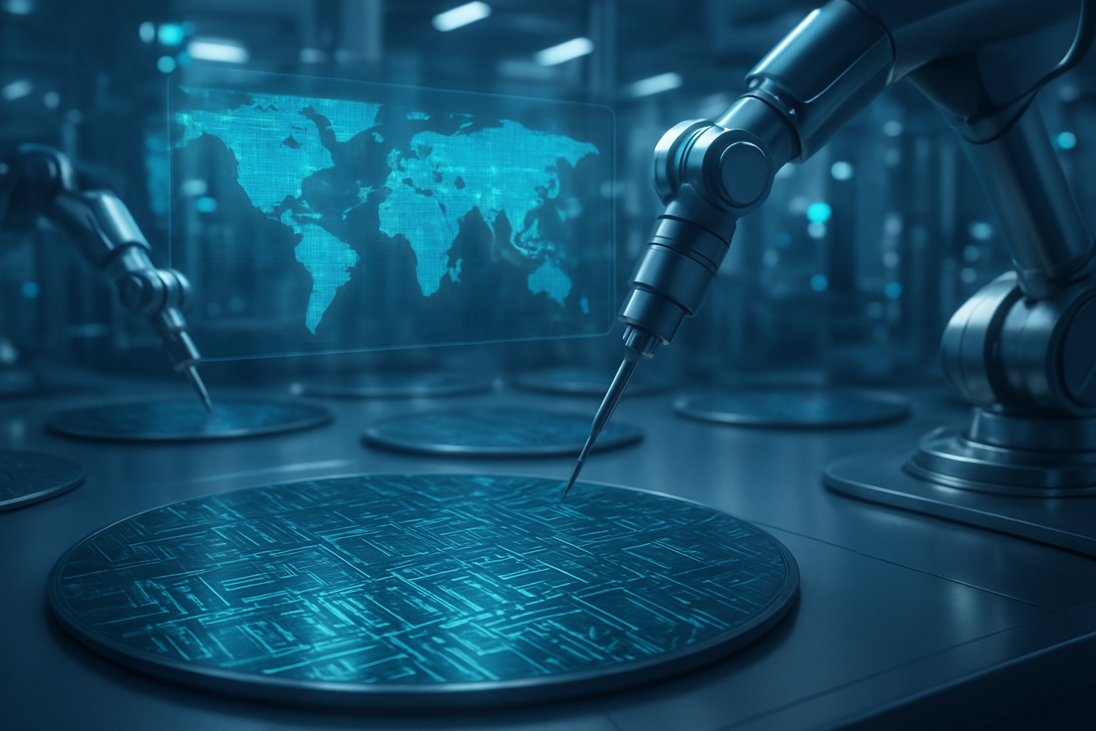
On the manufacturing front, AI is equally transformative. Predictive maintenance systems, powered by AI analytics, anticipate equipment failures in complex fabrication tools, drastically reducing unplanned downtime. Machine learning algorithms analyze vast production datasets to identify patterns leading to defects, improving overall yields and product quality, with some reports indicating up to a 30% reduction in yield detraction. Advanced defect detection systems, utilizing Convolutional Neural Networks (CNNs) and high-resolution imaging, can spot microscopic inconsistencies with up to 99% accuracy, surpassing human capabilities. Real-time process optimization, where AI models dynamically adjust manufacturing parameters, further enhances efficiency. Computational lithography, a critical step in chip production, has seen a 20x performance gain with the integration of NVIDIA's cuLitho library into platforms like Samsung's (KRX: 005930) Optical Proximity Correction (OPC) process. Moreover, the creation of "digital twins" for entire fabrication facilities, using platforms like NVIDIA Omniverse, allows for virtual simulation and optimization of production processes before physical implementation.
The initial reactions from the AI research community and industry experts have been overwhelmingly positive, albeit with a recognition of emerging challenges. The global semiconductor market is projected to grow by 15% in 2025, largely fueled by AI and high-performance computing (HPC), with the AI chip market alone expected to surpass $150 billion in 2025. This growth rate, dubbed "Hyper Moore's Law" by some, indicates that generative AI performance is doubling every six months. Major players like Synopsys, Intel (NASDAQ: INTC), AMD (NASDAQ: AMD), Samsung, and NVIDIA are making substantial investments, with collaborations such as Samsung and NVIDIA's plan to build a new "AI Factory" in October 2025, powered by over 50,000 NVIDIA GPUs. However, concerns persist regarding a critical talent shortfall, supply chain vulnerabilities exacerbated by geopolitical tensions, the concentrated economic benefits among a few top companies, and the immense power demands of AI workloads.
Reshaping the AI and Tech Landscape
The AI-driven growth in the semiconductor industry is profoundly reshaping the competitive landscape for AI companies, tech giants, and startups alike, creating new opportunities while intensifying existing rivalries in 2024 and 2025.
NVIDIA (NASDAQ: NVDA) remains the undisputed leader in AI hardware, particularly with its powerful GPUs (e.g., Blackwell GPUs), which are in high demand from major AI labs like OpenAI and tech giants such as Google (NASDAQ: GOOGL), Meta (NASDAQ: META), and Microsoft (NASDAQ: MSFT). Its comprehensive software ecosystem and networking capabilities further solidify its competitive edge. However, competitors are rapidly gaining ground. AMD (NASDAQ: AMD) is emerging as a strong challenger with its high-performance processors and MI300 series GPUs optimized for AI workloads, with OpenAI reportedly deploying AMD GPUs. Intel (NASDAQ: INTC) is heavily investing in its Gaudi 3 AI accelerators and adapting its CPU and GPU offerings for AI. TSMC (NYSE: TSM), as the leading pure-play foundry, is a critical enabler, producing advanced chips for nearly all major AI hardware developers and investing heavily in 3nm and 5nm production and CoWoS advanced packaging technology. Memory suppliers like Micron Technology (NASDAQ: MU), which produce High Bandwidth Memory (HBM), are also experiencing significant growth due to the immense bandwidth requirements of AI chips.
A significant trend is the rise of custom silicon among tech giants. Companies like Google (with its TPUs), Amazon (NASDAQ: AMZN) (with Inferentia and Trainium), and Microsoft are increasingly designing their own custom AI chips. This strategy aims to reduce reliance on external vendors, optimize performance for their specific AI workloads, and manage the escalating costs associated with procuring advanced GPUs. This move represents a potential disruption to traditional semiconductor vendors, as these hyperscalers seek greater control over their AI infrastructure. For startups, the landscape is bifurcated: specialized AI hardware startups like Groq (developing ultra-fast AI inference hardware) and Tenstorrent are attracting significant venture capital, while AI-driven design startups like ChipAgents are leveraging AI to automate chip-design workflows.
The competitive implications are clear: while NVIDIA maintains a strong lead, the market is becoming more diversified and competitive. The "silicon squeeze" means that economic profits are increasingly concentrated among a few top players, leading to pressure on others. Geopolitical factors, such as export controls on AI chips to China, continue to shape supply chain strategies and competitive positioning. The shift towards AI-optimized hardware means that companies failing to integrate these advancements risk falling behind. On-device AI processing, championed by edge AI startups and integrated by tech giants, promises to revolutionize consumer electronics, enabling more powerful, private, and real-time AI experiences directly on devices, potentially disrupting traditional cloud-dependent AI services and driving a major PC refresh cycle. The AI chip market, projected to surpass $150 billion in 2025, represents a structural transformation of how technology is built and consumed, with hardware re-emerging as a critical strategic differentiator.
A New Global Paradigm: Wider Significance
The AI-driven growth in the semiconductor industry is not merely an economic boom; it represents a new global paradigm with far-reaching societal impacts, critical concerns, and historical parallels that underscore its transformative nature in 2024 and 2025.
This era marks a symbiotic evolution where AI is not just a consumer of advanced chips but an active co-creator, fundamentally reshaping the very foundation upon which its future capabilities will be built. The demand for specialized AI chips—GPUs, ASICs, and NPUs—is soaring, driven by the need for parallel processing, lower latency, and reduced energy consumption. High-Bandwidth Memory (HBM) is seeing a surge, with its market revenue expected to reach $21 billion in 2025, a 70% year-over-year increase, highlighting its critical role in AI accelerators. This growth is pervasive, extending from hyperscale cloud data centers to edge computing devices like smartphones and autonomous vehicles, with half of all personal computers expected to feature NPUs by 2025. Furthermore, AI is revolutionizing the semiconductor value chain itself, with AI-driven Electronic Design Automation (EDA) tools compressing design cycles and AI in manufacturing enhancing process automation, yield optimization, and predictive maintenance.
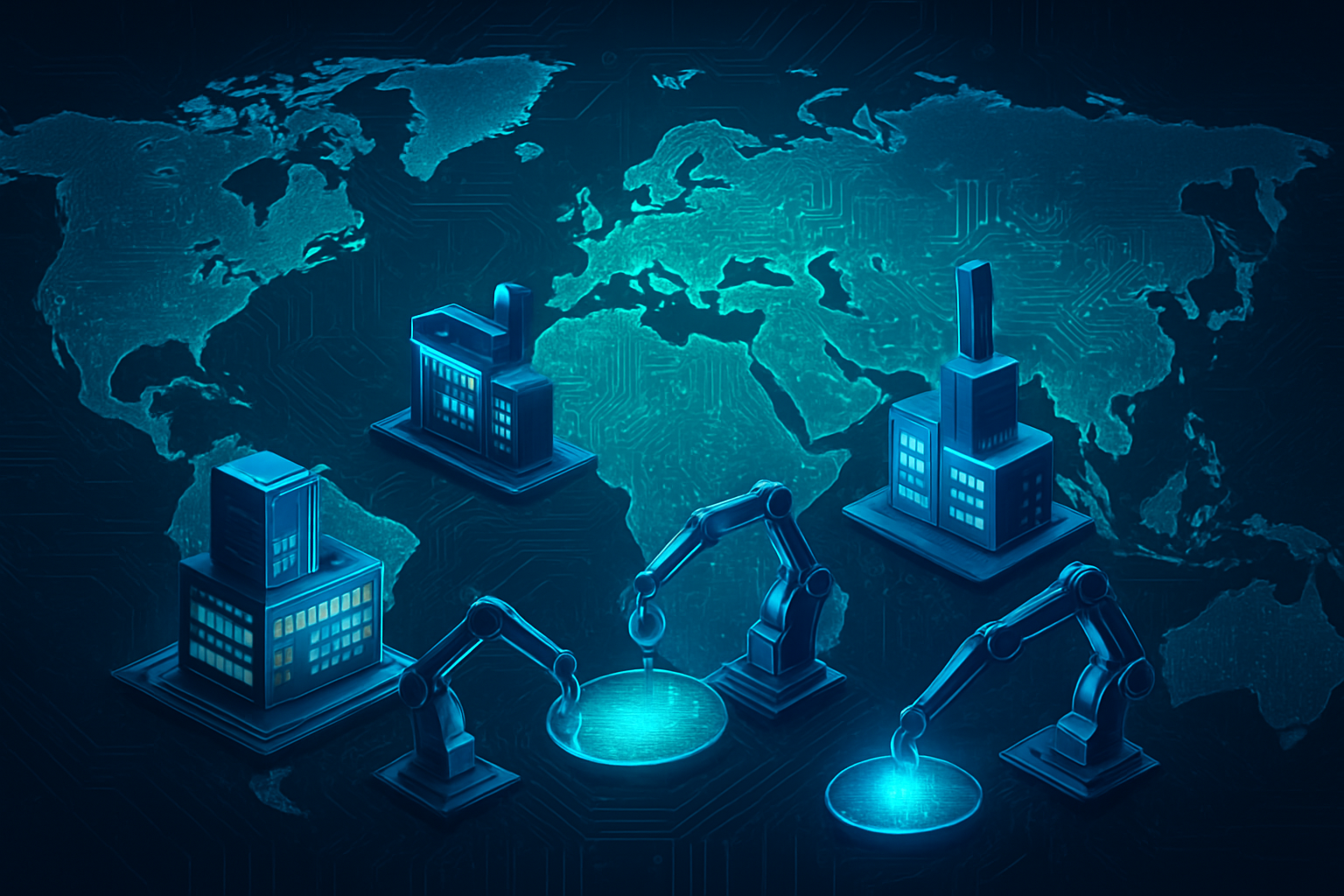
The wider societal impacts are profound. Economically, the integration of AI is expected to yield an annual increase of $85-$95 billion in earnings for the semiconductor industry by 2025, fostering new industries and job creation. However, geopolitical competition for technological leadership, particularly between the United States and China, is intensifying, with nations investing heavily in domestic manufacturing to secure supply chains. Technologically, AI-powered semiconductors are enabling transformative applications across healthcare (diagnostics, drug discovery), automotive (ADAS, autonomous vehicles), manufacturing (automation, predictive maintenance), and defense (autonomous drones, decision-support tools). Edge AI, by enabling real-time, low-power processing on devices, also has the potential to improve accessibility to advanced technology in underserved regions.
However, this rapid advancement brings critical concerns. Ethical dilemmas abound, including algorithmic bias, expanded surveillance capabilities, and the development of autonomous weapons systems (AWS), which pose profound questions regarding accountability and human judgment. Supply chain risks are magnified by the high concentration of advanced chip manufacturing in a few regions, primarily Taiwan and South Korea, coupled with escalating geopolitical tensions and export controls. The industry also faces a pressing shortage of skilled professionals. Perhaps one of the most significant concerns is energy consumption: AI workloads are extremely power-intensive, with estimates suggesting AI could account for 20% of data center power consumption in 2024, potentially rising to nearly half by the end of 2025. This raises significant sustainability concerns and strains electrical grids worldwide. Additionally, increased reliance on AI hardware introduces new security vulnerabilities, as attackers may exploit specialized hardware through side-channel attacks, and AI itself can be leveraged by threat actors for more sophisticated cyberattacks.
Comparing this to previous AI milestones, the current era is arguably as significant as the advent of deep learning or the development of powerful GPUs for parallel processing. It marks a "self-improving system" where AI acts as its own engineer, accelerating the very foundation upon which it stands. This phase differs from earlier technological breakthroughs where hardware primarily facilitated new applications; today, AI is driving innovation within the hardware development cycle itself, fostering a virtuous cycle of technological advancement. This shift signifies AI's transition from theoretical capabilities to practical, scalable, and pervasive intelligence, redefining the foundation of future AI.
The Horizon: Future Developments and Challenges
The symbiotic relationship between AI and semiconductors is poised to drive aggressive growth and innovation through 2025 and beyond, leading to a landscape of continuous evolution, novel applications, and persistent challenges. Experts anticipate a sustained "AI Supercycle" that will redefine technological capabilities.
In the near term, the global semiconductor market is projected to surpass $600 billion in 2025, with some forecasts reaching $697 billion. The AI semiconductor market specifically is expected to expand by over 30% in 2025. Generative AI will remain a primary catalyst, with its performance doubling every six months. This will necessitate continued advancements in specialized AI accelerators, custom silicon, and innovative memory solutions like HBM4, anticipated in late 2025. Data centers and cloud computing will continue to be major drivers, but there will be an increasing focus on edge AI, requiring low-power, high-performance chips for real-time processing in autonomous vehicles, industrial automation, and smart devices. Long-term, innovations like 3D chip stacking, chiplets, and advanced process nodes (e.g., 2nm) will become critical to enhance chip density, reduce latency, and improve power efficiency. AI itself will play an increasingly vital role in designing the next generation of AI chips, potentially discovering novel architectures beyond human engineers' current considerations.
Potential applications on the horizon are vast. Autonomous systems will heavily rely on edge AI chips for real-time decision-making. Smart devices and IoT will integrate more powerful and energy-efficient AI directly on the device. Healthcare and defense will see further AI-integrated applications driving demand for specialized chips. The emergence of neuromorphic computing, designed to mimic the human brain, promises ultra-energy-efficient processing for pattern recognition. While still long-term, quantum computing could also significantly impact semiconductors by solving problems currently beyond classical computers.
However, several significant challenges must be addressed. Energy consumption and heat dissipation remain critical issues, with AI workloads generating substantial heat and requiring advanced cooling solutions. TechInsights forecasts a staggering 300% increase in CO2 emissions from AI accelerators alone between 2025 and 2029, raising significant environmental concerns. Manufacturing complexity and costs are escalating, with modern fabrication plants costing up to $20 billion and requiring highly sophisticated equipment. Supply chain vulnerabilities, exacerbated by geopolitical tensions and the concentration of advanced chip manufacturing, continue to be a major risk. The industry also faces a persistent talent shortage, including AI and machine learning specialists. Furthermore, the high implementation costs for AI solutions and the challenge of data scarcity for effective AI model validation need to be overcome.
Experts predict a continued "AI Supercycle" with increased specialization and diversification of AI chips, moving beyond general-purpose GPUs to custom silicon for specific domains. Hybrid architectures and a blurring of the edge-cloud continuum are also expected. AI-driven EDA tools will further automate chip design, and AI will enable self-optimizing manufacturing processes. A growing focus on sustainability, including energy-efficient designs and renewable energy adoption, will be paramount. Some cloud AI chipmakers even anticipate the materialization of Artificial General Intelligence (AGI) around 2030, followed by Artificial Superintelligence (ASI), driven by the relentless performance improvements in AI hardware.
A New Era of Intelligent Computing
The AI-driven transformation of the semiconductor industry represents a monumental shift, marking a critical inflection point in the history of technology. This is not merely an incremental improvement but a fundamental re-architecture of how computing power is conceived, designed, and delivered. The unprecedented demand for specialized AI chips, coupled with AI's role as an active participant in its own hardware evolution, has created a "virtuous cycle of technological advancement" with few historical parallels.
The key takeaways are clear: explosive market expansion, driven by generative AI and data centers, is fueling demand for specialized chips and advanced memory. AI is revolutionizing every stage of the semiconductor value chain, from design automation to manufacturing optimization. This symbiotic relationship is extending computational boundaries and enabling next-generation AI capabilities across cloud and edge computing. Major players like NVIDIA, AMD, Intel, Samsung, and TSMC are at the forefront, but the landscape is becoming more competitive with the rise of custom silicon from tech giants and innovative startups.
The significance of this development in AI history cannot be overstated. It signifies AI's transition from a computational tool to a fundamental architect of its own future, pushing the boundaries of Moore's Law and enabling a world of ubiquitous intelligent computing. The long-term impact points towards a future where AI is embedded at every level of the hardware stack, fueling transformative applications across diverse sectors, and driving the global semiconductor market to unprecedented revenues, potentially reaching $1 trillion by 2030.
In the coming weeks and months, watch for continued announcements regarding new AI-powered design and manufacturing tools, including "ChipGPT"-like capabilities. Monitor developments in specialized AI accelerators, particularly those optimized for edge computing and low-power applications. Keep an eye on advancements in advanced packaging (e.g., 3D chip stacking) and material science breakthroughs. The demand for High-Bandwidth Memory (HBM) will remain a critical indicator, as will the expansion of enterprise edge AI deployments and the further integration of Neural Processing Units (NPUs) into consumer devices. Closely analyze the earnings reports of leading semiconductor companies for insights into revenue growth from AI chips, R&D investments, and strategic shifts. Finally, track global private investment in AI, as capital inflows will continue to drive R&D and market expansion in this dynamic sector. This era promises accelerated innovation, new partnerships, and further specialization as the industry strives to meet the insatiable computational demands of an increasingly intelligent world.
This content is intended for informational purposes only and represents analysis of current AI developments.
TokenRing AI delivers enterprise-grade solutions for multi-agent AI workflow orchestration, AI-powered development tools, and seamless remote collaboration platforms.
For more information, visit https://www.tokenring.ai/.