In a landmark strategic partnership announced on December 11-12, 2025, industrial titan Siemens (ETR: SIE) and leading specialty foundry GlobalFoundries (NASDAQ: GFS) revealed a groundbreaking collaboration aimed at integrating Artificial Intelligence (AI) to fundamentally transform chip manufacturing. This alliance is set to usher in a new era of enhanced efficiency, unprecedented automation, and heightened reliability across the semiconductor production lifecycle, from initial design to final product management.
The immediate significance of this announcement cannot be overstated. It represents a pivotal step in addressing the surging global demand for critical semiconductors, which are the bedrock of advanced technologies such as AI, autonomous systems, defense, energy, and connectivity. By embedding AI deeply into the fabrication process, Siemens and GlobalFoundries are not just optimizing production; they are strategically fortifying the global supercomputing ecosystem and bolstering regional chip independence, ensuring a more robust and predictable supply chain for the increasingly complex chips vital for national leadership in advanced technologies.
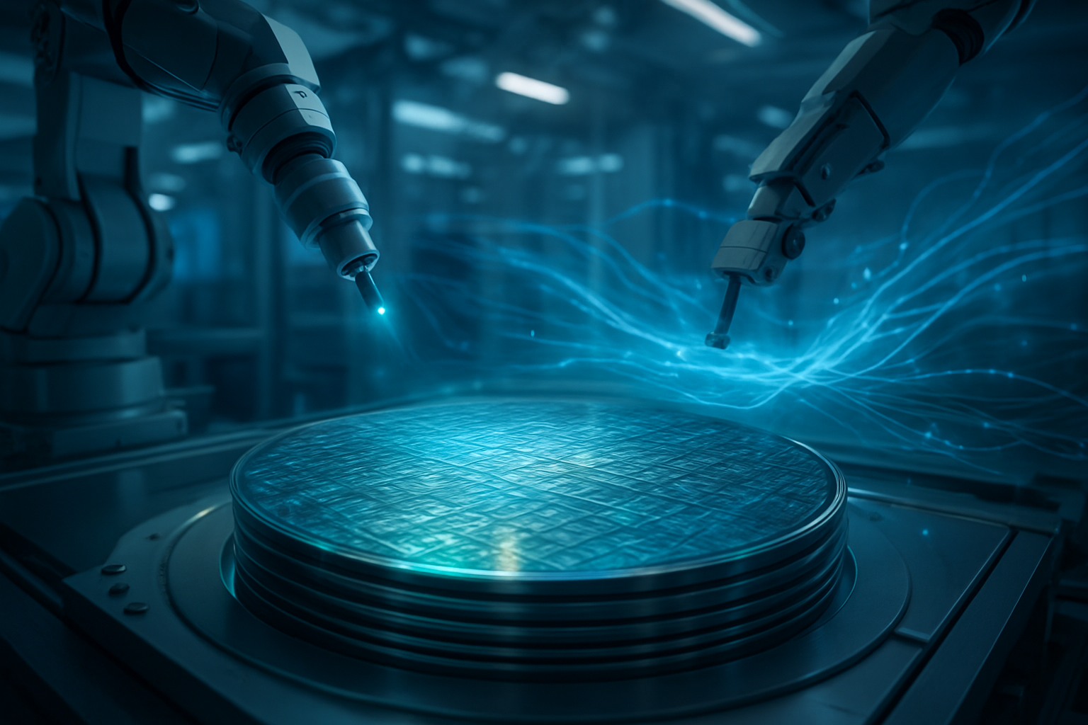
AI-Powered Precision: A New Era for Chip Production
This strategic collaboration between Siemens and GlobalFoundries is set to revolutionize semiconductor manufacturing through a deep integration of AI-driven technologies. At its core, the partnership will deploy AI-enabled software, sophisticated sensors, and real-time control systems directly into the heart of fabrication facilities. Key technical capabilities include "Smart Fab Automation" for real-time optimization of production lines, "Predictive Maintenance" utilizing machine learning to anticipate and prevent equipment failures, and extensive use of "Digital Twins" to simulate and optimize manufacturing processes virtually before physical implementation.
Siemens brings to the table its comprehensive suite of industrial automation, energy, and digitalization technologies, alongside advanced software for chip design, manufacturing execution systems (MES), and product lifecycle management (PLM). GlobalFoundries contributes its specialized process technology and design expertise, notably from its MIPS company, which specializes in RISC-V processor IP, to accelerate the development of custom semiconductor solutions. This integrated approach is a stark departure from previous methods, which largely relied on static automation and reactive problem-solving. The new AI systems are proactive and learning, capable of predicting failures, optimizing processes in real-time, and even self-correcting, thereby drastically reducing variability and minimizing production delays. Initial reactions from the AI research community and industry experts have been overwhelmingly positive, hailing the partnership as a "blueprint" for future fabs and a "pivotal transition from theoretical AI capabilities to tangible, real-world impact" on the foundational semiconductor industry.
Reshaping the Tech Landscape: Impact on AI Giants and Startups
The strategic partnership between Siemens and GlobalFoundries is poised to send ripples across the tech industry, impacting AI companies, tech giants, and startups alike. Both Siemens (ETR: SIE) and GlobalFoundries (NASDAQ: GFS) stand as primary beneficiaries, with Siemens solidifying its leadership in industrial AI and GlobalFoundries gaining a significant competitive edge through enhanced efficiency, reliability, and sustainability in its offerings. Customers of GlobalFoundries, particularly those in the high-growth AI, HPC, and automotive sectors, will benefit from improved production quality, predictability, and potentially lower costs of specialized semiconductors.
For major AI labs and tech companies, the competitive implications are substantial. Those leveraging the outputs of this partnership will gain a significant advantage through more reliable, energy-efficient, and high-yield semiconductor components. Conversely, competitors lacking similar AI-driven manufacturing strategies may find themselves at a disadvantage, pressured to make significant investments in AI integration to remain competitive. This collaboration also strengthens the foundational AI infrastructure by providing better hardware for training advanced AI models and deploying them at scale.
The partnership could disrupt existing products and services by setting a new benchmark for semiconductor manufacturing excellence. Less integrated fab management systems and traditional industrial automation solutions may face accelerated obsolescence. Furthermore, the availability of more reliable and high-performance chips could raise customer expectations for quality and lead times, pressing chip designers and foundries that cannot meet these new standards. Strategically, this alliance positions both companies to capitalize on the increasing global demand for localized and resilient semiconductor supply chains, bolstering regional chip independence and contributing to geopolitical advantages.
A Broader Horizon: AI's Role in Global Semiconductor Resilience
This Siemens GlobalFoundries partnership fits squarely within the broader AI landscape as a critical response to the escalating demand for AI chips and the increasing complexity of modern chip manufacturing. It signifies the maturation of industrial AI, moving beyond theoretical applications to practical, large-scale implementation in foundational industries. The collaboration also aligns perfectly with the Industry 4.0 movement, emphasizing smart manufacturing, comprehensive digitalization, and interconnected systems across the entire semiconductor lifecycle.
The wider impacts of this development are multifaceted. Technologically, it promises enhanced manufacturing efficiency and reliability, with projections of up to a 40% reduction in downtime and a 32% improvement in product quality. Economically, it aims to strengthen supply chain resilience and facilitate localized manufacturing, particularly in strategic regions like the US and Europe, thereby reducing geopolitical vulnerabilities. Furthermore, the integration of AI-guided energy systems in fabs will contribute to sustainability goals by lowering production costs and reducing the carbon footprint. This initiative also accelerates innovation, allowing for faster time-to-market for new chips and potentially extending AI-driven capabilities to other advanced industries like robotics and energy systems.
However, potential concerns include the technical complexity of integrating advanced AI with legacy infrastructure, the scarcity and security of proprietary manufacturing data, the need to address skill gaps in the workforce, and the substantial costs associated with this transition. Compared to previous AI milestones, such as AI in Electronic Design Automation (EDA) tools that reduced chip design times, this partnership represents a deeper, more comprehensive integration of AI into the physical manufacturing process itself. It marks a shift from reactive to proactive manufacturing and focuses on creating "physical AI chips at scale," where AI is used not only to make chips more efficiently but also to power the expansion of AI into the physical world.
The Road Ahead: Future Developments in Smart Fabs
In the near term, the Siemens GlobalFoundries AI partnership is expected to focus on the comprehensive deployment and optimization of AI-driven predictive maintenance and digital twin technologies within GlobalFoundries' fabrication plants. This will lead to tangible improvements in equipment uptime and overall manufacturing yield, with initial deployment results and feature announcements anticipated in the coming months. The immediate goals are to solidify smart fab automation, enhance process control, and establish robust, AI-powered systems for anticipating equipment failures.
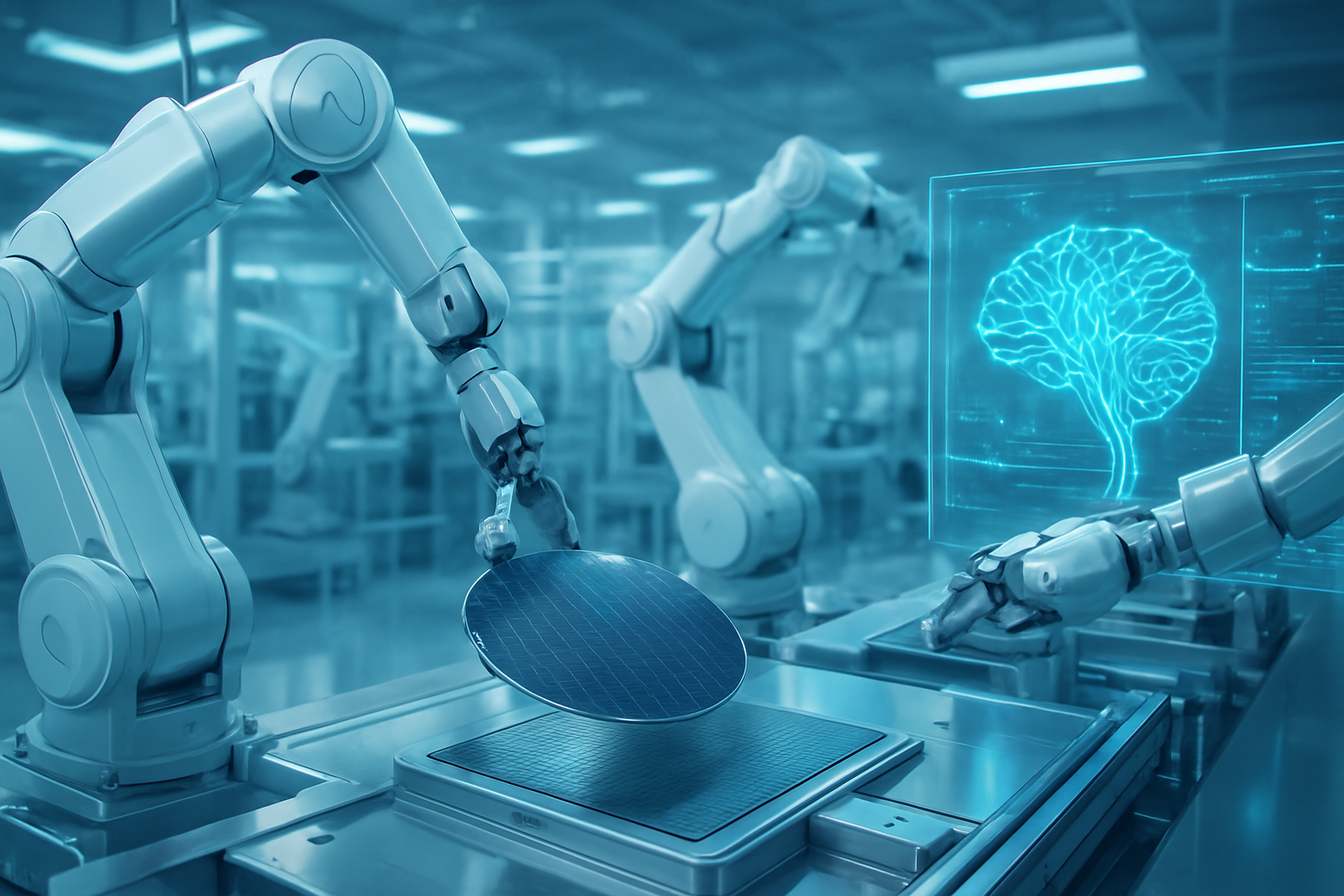
Looking further ahead, the long-term vision is to establish fully autonomous and intelligent fabs that operate with minimal human intervention, driven by AI-enabled software, real-time sensor feedback, and advanced robotics. This will lead to a more efficient, resilient, and sustainable global semiconductor ecosystem capable of meeting the escalating demands of an AI-driven future. Potential applications on the horizon include rapid prototyping and mass production of highly specialized AI accelerators, self-optimizing chips that dynamically adjust design parameters based on real-time feedback, and advanced AI algorithms for defect detection and quality control. Experts predict a continued surge in demand for AI-optimized facilities, driving accelerated investment and a new era of hardware-software co-design specifically tailored for AI.
Despite the immense potential, several challenges need to be addressed. These include the complex integration with legacy infrastructure, ensuring AI safety and standardization, developing a highly skilled workforce, mitigating cybersecurity vulnerabilities, and managing the extreme precision and cost associated with advanced process nodes. The industry will also need to focus on power and thermal management for high-performance AI chips and ensure the explainability and validation of AI models in critical manufacturing processes. Experts emphasize that AI will primarily augment human engineers, providing predictive insights and automated optimization tools, rather than entirely replacing human expertise.
A Defining Moment for AI in Industry
The strategic partnership between Siemens (ETR: SIE) and GlobalFoundries (NASDAQ: GFS) represents a defining moment in the application of AI to industrial processes, particularly within the critical semiconductor manufacturing sector. The key takeaways underscore a profound shift towards AI-driven automation, predictive maintenance, and comprehensive digitalization, promising unprecedented levels of efficiency, reliability, and supply chain resilience. This collaboration is not merely an incremental improvement; it signifies a fundamental re-imagining of how chips are designed and produced.
In the annals of AI history, this alliance will likely be remembered as a pivotal moment where AI transitioned from primarily data-centric applications to deeply embedded, real-world industrial transformation. Its long-term impact is expected to be transformative, fostering a more robust, sustainable, and regionally independent global semiconductor ecosystem. By setting a new benchmark for smart fabrication facilities, it has the potential to become a blueprint for AI integration across other advanced manufacturing sectors, accelerating innovation and strengthening national leadership in AI and advanced technologies.
In the coming weeks and months, industry observers should closely monitor the initial deployment results from GlobalFoundries' fabs, which will provide concrete evidence of the partnership's effectiveness. Further announcements regarding specific AI-powered tools and features are highly anticipated. It will also be crucial to observe how competing foundries and industrial automation firms respond to this new benchmark, as well as the ongoing efforts to address challenges such as workforce development and cybersecurity. The success of this collaboration will not only shape the future of chip manufacturing but also serve as a powerful testament to AI's transformative potential across the global industrial landscape.
This content is intended for informational purposes only and represents analysis of current AI developments.
TokenRing AI delivers enterprise-grade solutions for multi-agent AI workflow orchestration, AI-powered development tools, and seamless remote collaboration platforms.
For more information, visit https://www.tokenring.ai/.