Tag: Chip Quality

  • Cohu, Inc. Navigates Semiconductor Downturn with Strategic Focus on AI and Advanced Chip Quality Assurance

    Cohu, Inc. Navigates Semiconductor Downturn with Strategic Focus on AI and Advanced Chip Quality Assurance

    Cohu, Inc. (NASDAQ: COHU), a global leader in semiconductor test and inspection solutions, is demonstrating remarkable resilience and strategic foresight amidst a challenging cyclical downturn in the semiconductor industry. While recent financial reports reflect the broader market's volatility, Cohu's unwavering commitment to innovation in chip quality assurance, particularly in high-growth areas like Artificial Intelligence (AI) and High Bandwidth Memory (HBM) testing, underscores its critical importance to the future of technology. The company's strategic initiatives, including key acquisitions and new product launches, are not only bolstering its market position but also ensuring the reliability and performance of the next generation of semiconductors that power our increasingly AI-driven world.

    Cohu's indispensable role lies in providing the essential equipment and services that optimize semiconductor manufacturing yield and productivity. From advanced test handlers and burn-in equipment to sophisticated inspection and metrology platforms, Cohu’s technologies are the bedrock upon which chip manufacturers build trust in their products. As the demand for flawless, high-performance chips escalates across automotive, industrial, and data center sectors, Cohu's contributions to rigorous testing and defect detection are more vital than ever, directly impacting the quality and longevity of electronic devices globally.

    Precision Engineering for Flawless Silicon: Cohu's Technical Edge in Chip Verification

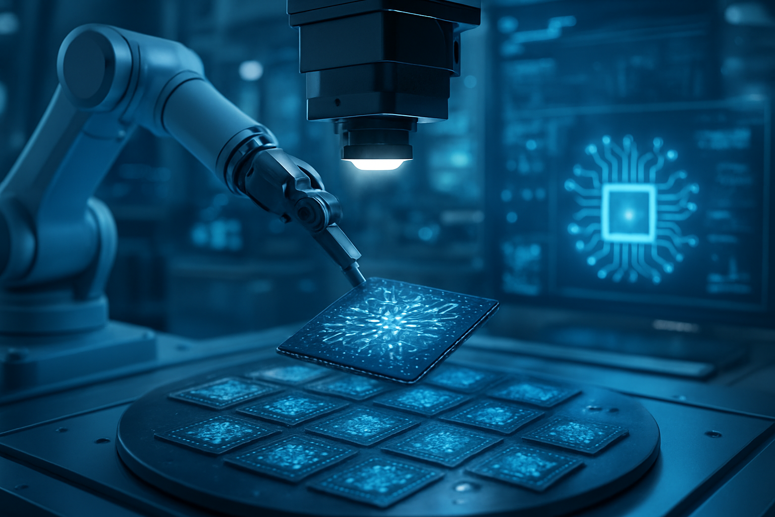
    Cohu's technological prowess is evident in its suite of advanced solutions designed to meet the escalating demands for chip quality and reliability. At the heart of its offerings are high-precision test and handling systems, which include sophisticated pick-and-place semiconductor test handlers, burn-in equipment, and thermal sub-systems. These systems are not merely components in a production line; they are critical gatekeepers, rigorously testing chips under diverse and extreme conditions to identify even the most minute defects and ensure flawless functionality before they reach end-user applications.

    A significant advancement in Cohu's portfolio is the Krypton inspection and metrology platform, launched in May 2024. This system represents a leap forward in optical inspection, capable of detecting defects as small as 1 µm with enhanced throughput and uptime. Its introduction is particularly timely, addressing the increasing quality demands from the automotive and industrial markets where even microscopic flaws can have catastrophic consequences. The Krypton platform has already secured an initial design-win, projecting an estimated $100 million revenue opportunity over the next five years. Furthermore, Cohu's Neon HBM inspection systems are gaining significant traction in the rapidly expanding AI data center markets, where the integrity of high-bandwidth memory is paramount for AI accelerators. The company projects these solutions to generate $10-$11 million in revenue in 2025, highlighting their direct relevance to the AI boom.

    Cohu differentiates itself from previous approaches and existing technologies through its integrated approach to thermal management and data analytics. The Eclipse platform, for instance, incorporates T-Core Active Thermal Control, providing precise thermal management up to an impressive 3kW dissipation with rapid ramp rates. This capability is crucial for testing high-performance devices, where temperature fluctuations can significantly impact test repeatability and overall yield. By ensuring stable and precise thermal environments, Eclipse improves the accuracy of testing and lowers the total cost of ownership for manufacturers. Complementing its hardware, Cohu's DI-Core™ Data Analytics suite offers real-time online performance monitoring and process control. This software platform is a game-changer, improving equipment utilization, enabling predictive maintenance, and integrating data from testers, handlers, and test contactors. Such integrated analytics are vital for identifying and resolving quality issues proactively, preventing significant production losses and safeguarding reputations in a highly competitive market. Initial reactions from the AI research community and industry experts emphasize the growing need for such robust, integrated test and inspection solutions, especially as chip complexity and performance demands continue to soar with the proliferation of AI.

    Cohu's Strategic Edge: Fueling the AI Revolution and Reshaping the Semiconductor Landscape

    Cohu's strategic advancements in semiconductor test and inspection are poised to significantly benefit a wide array of companies, particularly those at the forefront of the Artificial Intelligence revolution and high-performance computing. Chip designers like NVIDIA (NASDAQ: NVDA), AMD (NASDAQ: AMD), and Intel (NASDAQ: INTC), who are constantly pushing the boundaries of AI chip performance, stand to gain immensely from Cohu's enhanced quality assurance technologies. Their ability to deliver flawless, high-bandwidth memory and advanced processors directly relies on the precision and reliability of testing solutions like Cohu's Neon HBM inspection systems and the Eclipse platform. Furthermore, contract manufacturers and foundries such as TSMC (NYSE: TSM) and Samsung (KRX: 005930) will leverage Cohu's equipment to optimize their production yields and maintain stringent quality controls for their diverse client base, including major tech giants.

    The competitive implications for major AI labs and tech companies are substantial. As AI models become more complex and demand greater computational power, the underlying hardware must be impeccably reliable. Companies that can consistently source or produce higher-quality, more reliable AI chips will gain a significant competitive advantage in terms of system performance, energy efficiency, and overall innovation velocity. Cohu's offerings, by minimizing chip defects and ensuring optimal performance, directly contribute to this advantage. This development could potentially disrupt existing products or services that rely on less rigorous testing protocols, pushing the entire industry towards higher quality standards.

    In terms of market positioning and strategic advantages, Cohu is actively carving out a niche in the most critical and fastest-growing segments of the semiconductor market. Its acquisition of Tignis, Inc. in January 2025, a provider of AI process control and analytics software, is a clear strategic move to expand its analytics offerings and integrate AI directly into its quality control solutions. This acquisition is expected to significantly boost Cohu's software revenue, projecting 50% or more annual growth over the next three years. By focusing on AI and HBM testing, as well as the silicon carbide (SiC) markets driven by electric vehicles and renewable energy, Cohu is aligning itself with the mega-trends shaping the future of technology. Its recurring revenue model, comprising consumables, services, and software subscriptions, provides a stable financial base, acting as a crucial buffer against the inherent volatility of the semiconductor industry cycle and solidifying its strategic advantage.

    Cohu's Role in the Broader AI Landscape: Setting New Standards for Reliability

    Cohu's advancements in semiconductor test and inspection are not merely incremental improvements; they represent a fundamental strengthening of the foundation upon which the broader AI landscape is being built. As AI models become more sophisticated and pervasive, from autonomous vehicles to advanced robotics and enterprise-grade cloud computing, the demand for absolutely reliable and high-performance silicon is paramount. Cohu's technologies fit perfectly into this trend by ensuring that the very building blocks of AI – the processors, memory, and specialized accelerators – meet the highest standards of quality and functionality. This proactive approach to chip quality is critical, as even minor defects in AI hardware can lead to significant computational errors, system failures, and substantial financial losses, thereby impacting the trustworthiness and widespread adoption of AI solutions.

    The impacts of Cohu's work extend beyond just performance; they touch upon safety and ethical considerations in AI. For instance, in safety-critical applications like self-driving cars, where AI decisions have direct life-or-death implications, the reliability of every chip is non-negotiable. Cohu's rigorous testing and inspection processes contribute directly to mitigating potential concerns related to hardware-induced failures in AI systems. By improving yield and detecting defects early, Cohu helps reduce waste and increase the efficiency of semiconductor manufacturing, contributing to more sustainable practices within the tech industry. This development can be compared to previous AI milestones that focused on software breakthroughs; Cohu's work highlights the equally critical, albeit often less visible, hardware foundation that underpins all AI progress. It underscores a growing industry recognition that robust hardware is just as vital as innovative algorithms for the successful deployment of AI at scale.

    Potential concerns, however, might arise from the increasing complexity and cost of such advanced testing equipment. As chips become more intricate, the resources required for comprehensive testing also grow, potentially creating barriers for smaller startups or leading to increased chip costs. Nevertheless, the long-term benefits of enhanced reliability and reduced field failures likely outweigh these initial investments. Cohu's focus on recurring revenue streams through software and services also provides a pathway for managing these costs over time. This emphasis on chip quality assurance sets a new benchmark, demonstrating that as AI pushes the boundaries of computation, the industry must simultaneously elevate its standards for hardware integrity, ensuring that the promise of AI is built on a bedrock of unwavering reliability.

    The Road Ahead: Anticipating Cohu's Impact on Future AI Hardware

    Looking ahead, the trajectory of Cohu's innovations points towards several exciting near-term and long-term developments that will profoundly impact the future of AI hardware. In the near term, we can expect to see further integration of AI directly into Cohu's testing and inspection platforms. The acquisition of Tignis is a clear indicator of this trend, suggesting that AI-powered analytics will become even more central to predictive maintenance, real-time process control, and identifying subtle defect patterns that human operators or traditional algorithms might miss. This will lead to more intelligent, self-optimizing test environments that can adapt to new chip designs and manufacturing challenges with unprecedented speed and accuracy.

    In the long term, Cohu's focus on high-growth markets like HBM and SiC testing will solidify its position as a critical enabler for next-generation AI and power electronics. We can anticipate the development of even more advanced thermal management solutions to handle the extreme power densities of future AI accelerators, along with novel inspection techniques capable of detecting nanoscale defects in increasingly complex 3D-stacked architectures. Potential applications and use cases on the horizon include highly customized testing solutions for neuromorphic chips, quantum computing components, and specialized AI hardware designed for edge computing, where reliability and low power consumption are paramount.

    However, several challenges need to be addressed. The relentless pace of Moore's Law, combined with the increasing diversity of chip architectures (e.g., chiplets, heterogeneous integration), demands continuous innovation in test methodologies. The cost of testing itself could become a significant factor, necessitating more efficient and parallelized test strategies. Furthermore, the global talent pool for highly specialized test engineers and AI integration experts will need to grow to keep pace with these advancements. Experts predict that Cohu, along with its competitors, will increasingly leverage digital twin technology and advanced simulation to design and optimize test flows, further blurring the lines between virtual and physical testing. The industry will also likely see a greater emphasis on "design for testability" at the earliest stages of chip development to simplify the complex task of ensuring quality.

    A Cornerstone of AI's Future: Cohu's Enduring Significance

    In summary, Cohu, Inc.'s performance and strategic initiatives underscore its indispensable role in the semiconductor ecosystem, particularly as the world increasingly relies on Artificial Intelligence. Despite navigating the cyclical ebbs and flows of the semiconductor market, Cohu's unwavering commitment to innovation in test and inspection is ensuring the quality and reliability of the chips that power the AI revolution. Key takeaways include its strategic pivot towards high-growth segments like HBM and SiC, the integration of AI into its own process control through acquisitions like Tignis, and the continuous development of advanced platforms such as Krypton and Eclipse that set new benchmarks for defect detection and thermal management.

    Cohu's contributions represent a foundational element in AI history, demonstrating that the advancement of AI is not solely about software algorithms but equally about the integrity and reliability of the underlying hardware. Its work ensures that the powerful computations performed by AI systems are built on a bedrock of flawless silicon, thereby enhancing performance, reducing failures, and accelerating the adoption of AI across diverse industries. The significance of this development cannot be overstated; without robust quality assurance at the chip level, the promise of AI would remain constrained by hardware limitations and unreliability.

    Looking ahead, the long-term impact of Cohu's strategic direction will be evident in the continued proliferation of high-performance, reliable AI systems. What to watch for in the coming weeks and months includes further announcements regarding the integration of Tignis's AI capabilities into Cohu's product lines, additional design-wins for its cutting-edge Krypton and Eclipse platforms, and the expansion of its presence in emerging markets. Cohu's ongoing efforts to enhance chip quality assurance are not just about business growth; they are about building a more reliable and trustworthy future for artificial intelligence.


    This content is intended for informational purposes only and represents analysis of current AI developments.

    TokenRing AI delivers enterprise-grade solutions for multi-agent AI workflow orchestration, AI-powered development tools, and seamless remote collaboration platforms.
    For more information, visit https://www.tokenring.ai/.

  • The New Era of Silicon: AI, Advanced Packaging, and Novel Materials Propel Chip Quality to Unprecedented Heights

    The New Era of Silicon: AI, Advanced Packaging, and Novel Materials Propel Chip Quality to Unprecedented Heights

    October 6, 2025 – The semiconductor industry is in the midst of a profound transformation, driven by an insatiable global demand for increasingly powerful, efficient, and reliable chips. This revolution, fueled by the synergistic advancements in Artificial Intelligence (AI), sophisticated packaging techniques, and the exploration of novel materials, is fundamentally reshaping the quality and capabilities of semiconductors across every application, from the smartphones in our pockets to the autonomous vehicles on our roads. As traditional transistor scaling faces physical limitations, these innovations are not merely extending Moore's Law but are ushering in a new era of chip design and manufacturing, crucial for the continued acceleration of AI and the broader digital economy.

    The immediate significance of these developments is palpable. The global semiconductor market is projected to reach an all-time high of $697 billion in 2025, with AI technologies alone expected to account for over $150 billion in sales. This surge is a direct reflection of the breakthroughs in chip quality, which are enabling faster innovation cycles, expanding the possibilities for new applications, and ensuring the reliability and security of critical systems in an increasingly interconnected world. The industry is witnessing a shift where quality, driven by intelligent design and manufacturing, is as critical as raw performance.

    The Technical Core: AI, Advanced Packaging, and Materials Redefine Chip Excellence

    The current leap in semiconductor quality is underpinned by a trifecta of technical advancements, each pushing the boundaries of what's possible.

    AI's Intelligent Hand in Chipmaking: AI, particularly machine learning (ML) and deep learning (DL), has become an indispensable tool across the entire semiconductor lifecycle. In design, AI-powered Electronic Design Automation (EDA) tools, such as Synopsys' (NASDAQ: SNPS) DSO.ai system, are revolutionizing workflows by automating complex tasks like layout generation, design optimization, and defect prediction. This drastically reduces time-to-market; a 5nm chip's optimization cycle, for instance, has reportedly shrunk from six months to six weeks. AI can explore billions of possible transistor arrangements, creating designs that human engineers might not conceive, leading to up to a 40% reduction in power efficiency and a 3x to 5x improvement in design productivity. In manufacturing, AI algorithms analyze vast amounts of real-time production data to optimize processes, predict maintenance needs, and significantly reduce defect rates, boosting yield rates by up to 30% for advanced nodes. For quality control, AI, ML, and deep learning are integrated into visual inspection systems, achieving over 99% accuracy in detecting, classifying, and segmenting defects, even at submicron and nanometer scales. Purdue University's recent research, for example, integrates advanced imaging with AI to detect minuscule defects, moving beyond traditional manual inspections to ensure chip reliability and combat counterfeiting. This differs fundamentally from previous rule-based or human-intensive approaches, offering unprecedented precision and efficiency.

    Advanced Packaging: Beyond Moore's Law: As traditional transistor scaling slows, advanced packaging has emerged as a cornerstone of semiconductor innovation, enabling continued performance improvements and reduced power consumption. This involves combining multiple semiconductor chips (dies or chiplets) into a single electronic package, rather than relying on a single monolithic die. 2.5D and 3D-IC packaging are leading the charge. 2.5D places components side-by-side on an interposer, while 3D-IC vertically stacks active dies, often using through-silicon vias (TSVs) for ultra-short signal paths. Techniques like TSMC's (NYSE: TSM) CoWoS (chip-on-wafer-on-substrate) and Intel's (NASDAQ: INTC) EMIB (embedded multi-die interconnect bridge) exemplify this, achieving interconnection speeds of up to 4.8 TB/s (e.g., NVIDIA (NASDAQ: NVDA) Hopper H100 with HBM stacks). Hybrid bonding is crucial for advanced packaging, achieving interconnect pitches in the single-digit micrometer range, a significant improvement over conventional microbump technology (40-50 micrometers), and bandwidths up to 1000 GB/s. This allows for heterogeneous integration, where different chiplets (CPUs, GPUs, memory, specialized AI accelerators) are manufactured using their most suitable process nodes and then combined, optimizing overall system performance and efficiency. This approach fundamentally differs from traditional packaging, which typically packaged a single die and relied on slower PCB connections, offering increased functional density, reduced interconnect distances, and improved thermal management.

    Novel Materials: The Future Beyond Silicon: As silicon approaches its inherent physical limitations, novel materials are stepping in to redefine chip performance. Wide-Bandgap (WBG) Semiconductors like Gallium Nitride (GaN) and Silicon Carbide (SiC) are revolutionizing power electronics. GaN boasts a bandgap of 3.4 eV (compared to silicon's 1.1 eV) and a breakdown field strength ten times higher, allowing for 10-100 times faster switching speeds and operation at higher voltages and temperatures. SiC offers similar advantages with three times higher thermal conductivity than silicon, crucial for electric vehicles and industrial applications. Two-Dimensional (2D) Materials such as graphene and molybdenum disulfide (MoS₂) promise higher electron mobility (graphene can be 100 times greater than silicon) for faster switching and reduced power consumption, enabling extreme miniaturization. High-k Dielectrics, like Hafnium Oxide (HfO₂), replace silicon dioxide as gate dielectrics, significantly reducing gate leakage currents (by more than an order of magnitude) and power consumption in scaled transistors. These materials offer superior electrical, thermal, and scaling properties that silicon cannot match, opening doors for new device architectures and applications. The AI research community and industry experts have reacted overwhelmingly positively to these advancements, hailing AI as a "game-changer" for design and manufacturing, recognizing advanced packaging as a "critical enabler" for high-performance computing, and viewing novel materials as essential for overcoming silicon's limitations.

    Industry Ripples: Reshaping the Competitive Landscape

    The advancements in semiconductor chip quality are creating a fiercely competitive and dynamic environment, profoundly impacting AI companies, tech giants, and agile startups.

    Beneficiaries Across the Board: Chip designers and vendors like NVIDIA (NASDAQ: NVDA), AMD (NASDAQ: AMD), and Intel (NASDAQ: INTC) are direct beneficiaries, with NVIDIA continuing its dominance in AI acceleration through its GPU architectures (Hopper, Blackwell) and the robust CUDA ecosystem. AMD is aggressively challenging with its Instinct GPUs and EPYC server processors, securing partnerships with cloud providers like Microsoft (NASDAQ: MSFT) and Oracle (NYSE: ORCL). Intel is investing in AI-specific accelerators (Gaudi 3) and advanced manufacturing (18A process). Foundries like TSMC (NYSE: TSM) and Samsung (KRX: 005930) are exceptionally well-positioned due to their leadership in advanced process nodes (3nm, 2nm) and cutting-edge packaging technologies like CoWoS, with TSMC doubling its CoWoS capacity for 2025. Semiconductor equipment suppliers such as ASML (NASDAQ: ASML), Applied Materials (NASDAQ: AMAT), Lam Research (NASDAQ: LRCX), and KLA Corp (NASDAQ: KLAC) are also seeing increased demand for their specialized tools. Memory manufacturers like Micron Technology (NASDAQ: MU), Samsung, and SK Hynix (KRX: 000660) are experiencing a recovery driven by the massive data storage requirements for AI, particularly for High-Bandwidth Memory (HBM).

    Competitive Implications: The continuous enhancement of chip quality directly translates to faster AI training, more responsive inference, and significantly lower power consumption, allowing AI labs to develop more sophisticated models and deploy them at scale cost-effectively. Tech giants like Apple (NASDAQ: AAPL), Google (NASDAQ: GOOGL), and Microsoft are increasingly designing their own custom AI chips (e.g., Google's TPUs) to gain a competitive edge through vertical integration, optimizing performance, efficiency, and cost for their specific AI workloads. This reduces reliance on external vendors and allows for tighter hardware-software co-design. Advanced packaging has become a crucial differentiator, and companies mastering or securing access to these technologies gain a significant advantage in building high-performance AI systems. NVIDIA's formidable hardware-software ecosystem (CUDA) creates a strong lock-in effect, making it challenging for rivals. The industry also faces intense talent wars for specialized researchers and engineers.

    Potential Disruption: Less sophisticated chip design, manufacturing, and inspection methods are rapidly becoming obsolete, pressuring companies to invest heavily in AI and computer vision R&D. There's a notable shift from general-purpose to highly specialized AI silicon (ASICs, NPUs, neuromorphic chips) optimized for specific AI tasks, potentially disrupting companies relying solely on general-purpose CPUs or GPUs for certain applications. While AI helps optimize supply chains, the increasing concentration of advanced component manufacturing makes the industry potentially more vulnerable to disruptions. The surging demand for compute-intensive AI workloads also raises energy consumption concerns, driving the need for more efficient chips and innovative cooling solutions. Critically, advanced packaging solutions are dramatically boosting memory bandwidth and reducing latency, directly overcoming the "memory wall" bottleneck that has historically constrained AI performance, accelerating R&D and making real-time AI applications more feasible.

    Wider Significance: A Foundational Shift for AI and Society

    These semiconductor advancements are foundational to the "AI Gold Rush" and represent a critical juncture in the broader technological evolution.

    Enabling AI's Exponential Growth: Improved chip quality directly fuels the "insatiable hunger" for computational power demanded by generative AI, large language models (LLMs), high-performance computing (HPC), and edge AI. Specialized hardware, optimized for neural networks, is at the forefront, enabling faster and more efficient AI training and inference. The AI chip market alone is projected to surpass $150 billion in 2025, underscoring this deep interdependency.

    Beyond Moore's Law: As traditional silicon scaling approaches its limits, advanced packaging and novel materials are extending performance scaling, effectively serving as the "new battleground" for semiconductor innovation. This shift ensures the continued progress of computing power, even as transistor miniaturization becomes more challenging. These advancements are critical enablers for other major technological trends, including 5G/6G communications, autonomous vehicles, the Internet of Things (IoT), and data centers, all of which require high-performance, energy-efficient chips.

    Broader Impacts:

    • Technological: Unprecedented performance, efficiency, and miniaturization are being achieved, enabling new architectures like neuromorphic chips that offer up to 1000x improvements in energy efficiency for specific AI inference tasks.
    • Economic: The global semiconductor market is experiencing robust growth, projected to reach $697 billion in 2025 and potentially $1 trillion by 2030. This drives massive investment and job creation, with over $500 billion invested in the U.S. chip ecosystem since 2020. New AI-driven products and services are fostering innovation across sectors.
    • Societal: AI-powered applications, enabled by these chips, are becoming more integrated into consumer electronics, autonomous systems, and AR/VR devices, potentially enhancing daily life and driving advancements in critical sectors like healthcare and defense. AI, amplified by these hardware improvements, has the potential to drive enormous productivity growth.

    Potential Concerns: Despite the benefits, several concerns persist. Geopolitical tensions and supply chain vulnerabilities, particularly between the U.S. and China, continue to create significant challenges, increasing costs and risking innovation. The high costs and complexity of manufacturing advanced nodes require heavy investment, potentially concentrating power among a few large players. A critical talent shortage in the semiconductor industry threatens to impede innovation. Despite efforts toward energy efficiency, the exponential growth of AI and data centers still demands significant energy, raising environmental concerns. Finally, as semiconductors enable more powerful AI, ethical implications around data privacy, algorithmic bias, and job displacement become more pressing.

    Comparison to Previous AI Milestones: These hardware advancements represent a distinct, yet interconnected, phase compared to previous AI milestones. Earlier breakthroughs were often driven by algorithmic innovations (e.g., deep learning). However, the current phase is characterized by a "profound shift" in the physical hardware itself, becoming the primary enabler for the "next wave of AI innovation." While previous milestones initiated new AI capabilities, current semiconductor improvements amplify and accelerate these capabilities, pushing them into new domains and performance levels. This era is defined by a uniquely symbiotic relationship where AI development necessitates advanced semiconductors, while AI itself is an indispensable tool for designing and manufacturing these next-generation processors.

    The Horizon: Future Developments and What's Next

    The semiconductor industry is poised for unprecedented advancements, with a clear roadmap for both the near and long term.

    Near-Term (2025-2030): Expect advanced packaging technologies like 2.5D and 3D-IC stacking, FOWLP, and chiplet integration to become standard, driving heterogeneous integration. TSMC's CoWoS capacity will continue to expand aggressively, and Cu-Cu hybrid bonding for 3D die stacking will see increased adoption. Continued miniaturization through EUV lithography will push transistor performance, with new materials and 3D structures extending capabilities for at least another decade. Customization of High-Bandwidth Memory (HBM) and other memory innovations like GDDR7 will be crucial for managing AI's massive data demands. A strong focus on energy efficiency will lead to breakthroughs in power components for edge AI and data centers.

    Long-Term (Beyond 2030): The exploration of materials beyond silicon will intensify. Wide-bandband semiconductors (GaN, SiC) will become indispensable for power electronics in EVs and 5G/6G. Two-dimensional materials (graphene, MoS₂, InSe) are long-term solutions for scaling limits, offering exceptional electrical conductivity and potential for novel device architectures and neuromorphic computing. Hybrid approaches integrating 2D materials with silicon or WBG semiconductors are predicted as an initial pathway to commercialization. System-level integration and customization will continue, and high-stack 3D DRAM mass production is anticipated around 2030.

    Potential Applications: Advanced chips will underpin generative AI and LLMs in cloud data centers, PCs, and smartphones; edge AI in autonomous vehicles and IoT devices; 5G/6G communications; high-performance computing; next-generation consumer electronics (AR/VR); healthcare devices; and even quantum computing.

    Challenges Ahead: Realizing these future developments requires overcoming significant hurdles: the immense technological complexity and cost of miniaturization; supply chain disruptions and geopolitical tensions; a critical and intensifying talent shortage; and the growing energy consumption and environmental impact of AI and semiconductor manufacturing.

    Expert Predictions: Experts predict AI will play an even more transformative role, automating design, optimizing manufacturing, enhancing reliability, and revolutionizing supply chain management. Advanced packaging, with its market forecast to rise at a robust 9.4% CAGR, is considered the "hottest topic," with 2.5D and 3D technologies dominating HPC and AI. Novel materials like GaN and SiC are seen as indispensable for power electronics, while 2D materials are long-term solutions for scaling limits, with hybrid approaches likely paving the way for commercialization.

    Comprehensive Wrap-Up: A New Dawn for Computing

    The advancements in semiconductor chip quality, driven by AI, advanced packaging, and novel materials, represent a pivotal moment in technological history. The key takeaway is the symbiotic relationship between these three pillars: AI not only consumes high-quality chips but is also an indispensable tool in their creation and validation. Advanced packaging and novel materials provide the physical foundation for the increasingly powerful, efficient, and specialized AI hardware demanded today. This trifecta is pushing performance boundaries beyond traditional scaling limits, improving quality through unprecedented precision, and fostering innovation for future computing paradigms.

    This development's significance in AI history cannot be overstated. Just as GPUs catalyzed the Deep Learning Revolution, the current wave of hardware innovation is essential for the continued scaling and widespread deployment of advanced AI. It unlocks unprecedented efficiencies, accelerates innovation, and expands AI's reach into new applications and extreme environments.

    The long-term impact is transformative. Chiplet-based designs are set to become the standard for complex, high-performance computing. The industry is moving towards fully autonomous manufacturing facilities, reshaping global strategies. Novel AI-specific hardware architectures, like neuromorphic chips, will offer vastly more energy-efficient AI processing, expanding AI's reach into new applications and extreme environments. While silicon will remain dominant in the near term, new electronic materials are expected to gradually displace it in mass-market devices from the mid-2030s, promising fundamentally more efficient and versatile computing. These innovations are crucial for mitigating AI's growing energy footprint and enabling future breakthroughs in autonomous systems, 5G/6G communications, electric vehicles, and even quantum computing.

    What to watch for in the coming weeks and months (October 2025 context):

    • Advanced Packaging Milestones: Continued widespread adoption of 2.5D and 3D hybrid bonding for high-performance AI and HPC systems, along with the maturation of the chiplet ecosystem and interconnect standards like UCIe.
    • HBM4 Commercialization: The full commercialization of HBM4 memory, expected in late 2025, will deliver another significant leap in memory bandwidth for AI accelerators.
    • TSMC's 2nm Production and CoWoS Expansion: TSMC's mass production of 2nm chips in Q4 2025 and its aggressive expansion of CoWoS capacity are critical indicators of industry direction.
    • Real-time AI Testing Deployments: The collaboration between Advantest (OTC: ATEYY) and NVIDIA, with NVIDIA selecting Advantest's ACS RTDI for high-volume production of Blackwell and next-generation devices, highlights the immediate impact of AI on testing efficiency and yield.
    • Novel Material Research: New reports and studies, such as Yole Group's Q4 2025 publications on "Glass Materials in Advanced Packaging" and "Polymeric Materials for Advanced Packaging," which will offer insights into emerging material opportunities.
    • Global Investment and Geopolitics: Continued massive investments in AI infrastructure and the ongoing influence of geopolitical risks and new export controls on the semiconductor supply chain.
    • India's Entry into Packaged Chips: Kaynes SemiCon is on track to become the first company in India to deliver packaged semiconductor chips by October 2025, marking a significant milestone for India's semiconductor ambitions and global supply chain diversification.

    This content is intended for informational purposes only and represents analysis of current AI developments.

    TokenRing AI delivers enterprise-grade solutions for multi-agent AI workflow orchestration, AI-powered development tools, and seamless remote collaboration platforms. For more information, visit https://www.tokenring.ai/.