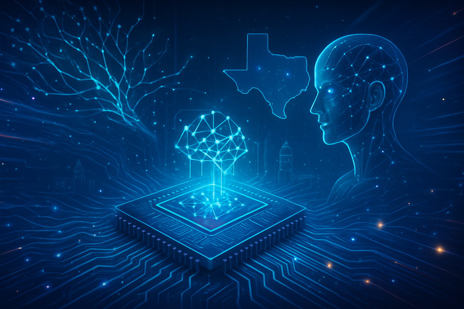
Texas universities are at the vanguard of a transformative movement, meticulously shaping the next generation of chip technology through an extensive network of semiconductor research and development initiatives. Bolstered by unprecedented state and federal investments, including monumental allocations from the CHIPS Act, these institutions are driving innovation in advanced materials, novel device architectures, cutting-edge manufacturing processes, and critical workforce development, firmly establishing Texas as an indispensable leader in the global resurgence of the U.S. semiconductor industry. This directly underpins the future capabilities of artificial intelligence and myriad other advanced technologies.
The immediate significance of these developments cannot be overstated. By focusing on domestic R&D and manufacturing, Texas is playing a crucial role in fortifying national security and economic resilience, reducing reliance on volatile overseas supply chains. The synergy between academic research and industrial application is accelerating the pace of innovation, promising a new era of more powerful, energy-efficient, and specialized chips that will redefine the landscape of AI, autonomous systems, and high-performance computing.
Unpacking the Technical Blueprint: Innovation from Lone Star Labs
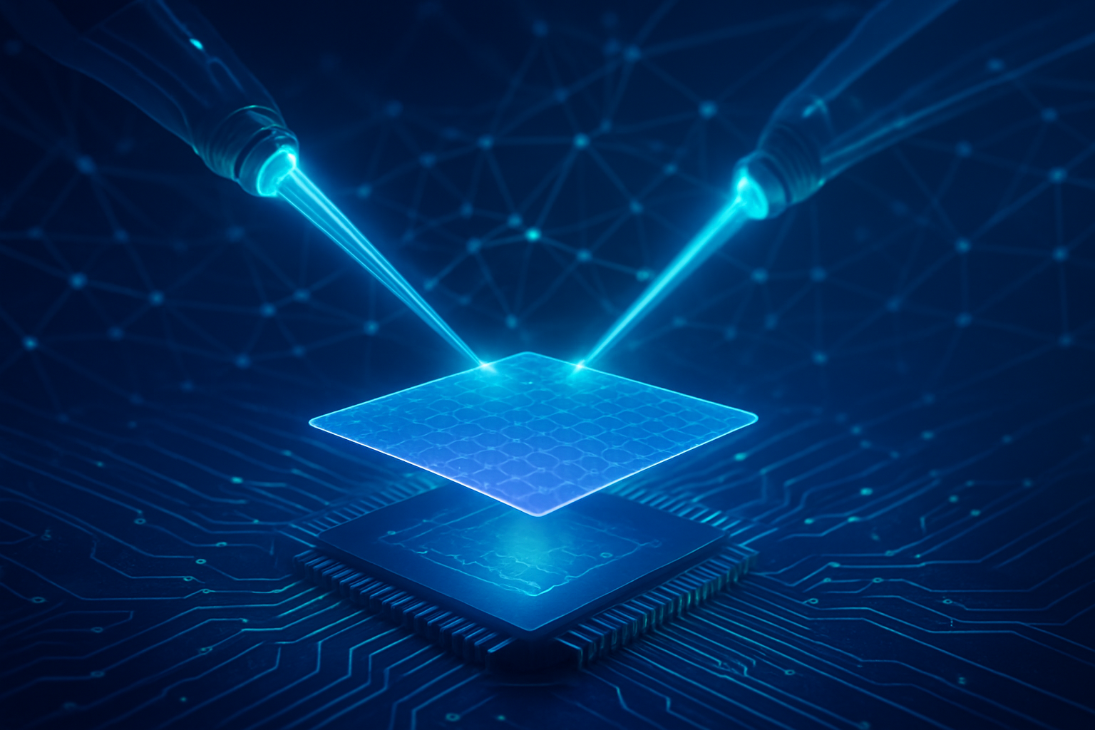
The technical depth of Texas universities' semiconductor research is both broad and groundbreaking, addressing fundamental challenges in chip design and fabrication. At the forefront is the University of Texas at Austin (UT Austin), which spearheads the Texas Institute for Electronics (TIE), a public-private consortium that secured an $840 million grant from the Defense Advanced Research Project Agency (DARPA). This funding is dedicated to developing next-generation high-performing semiconductor microsystems, with a particular emphasis on 3D Heterogeneous Integration (3DHI). This advanced fabrication technology allows for the precision assembly of diverse materials and components into a single microsystem, dramatically enhancing performance and efficiency compared to traditional planar designs. TIE is establishing a national open-access R&D and prototyping fabrication facility, democratizing access to cutting-edge tools.
UT Austin researchers have also unveiled Holographic Metasurface Nano-Lithography (HMNL), a revolutionary 3D printing technique for semiconductor components. This DARPA-supported project, with a $14.5 million award, promises to design and produce complex electronic structures at speeds and complexities previously unachievable, potentially shortening production cycles from months to days. Furthermore, UT Austin's "GENIE-RFIC" project, with anticipated CHIPS Act funding, is exploring AI-driven tools for rapid "inverse" designs of Radio Frequency Integrated Circuits (RFICs), optimizing circuit topologies for both Silicon CMOS and Gallium Nitride (GaN) Monolithic Microwave Integrated Circuits (MMICs). The establishment of the Quantum-Enhanced Semiconductor Facility (QLab), funded by a $4.8 million grant from the Texas Semiconductor Innovation Fund (TSIF), further highlights UT Austin's commitment to integrating quantum science into semiconductor metrology for advanced manufacturing.
Meanwhile, Texas A&M University is making significant strides in areas such as neuromorphic materials and scientific machine learning/AI for energy-efficient computing, including applications in robotics and biomedical devices. The Texas Semiconductor Institute, established in May 2023, coordinates responses to state and federal CHIPS initiatives, with research spanning CHIPS-in-Space, disruptive lithography, metrology, novel materials, and digital twins. The Texas A&M University System is slated to receive $226.4 million for chip fabrication R&D, focusing on new chemistry and processes, alongside an additional $200 million for quantum and AI chip fabrication.
Other institutions are contributing unique expertise. The University of North Texas (UNT) launched the Center for Microelectronics in Extreme Environments (CMEE) in March 2025, specializing in semiconductors for high-power electronic devices designed to perform in harsh conditions, crucial for defense and space applications. Rice University secured a $1.9 million National Science Foundation (NSF) grant for research on multiferroics to create ultralow-energy logic-in-memory computing devices, addressing the immense energy consumption of future electronics. The University of Texas at Dallas (UT Dallas) leads the North Texas Semiconductor Institute (NTxSI), focusing on materials and devices for harsh environments, and received a $1.9 million NSF FuSe2 grant to design indium-based materials for advanced Extreme Ultraviolet (EUV) lithography. Texas Tech University is concentrating on wide and ultra-wide bandgap semiconductors for high-power applications, securing a $6 million U.S. Department of Defense grant for advanced materials and devices targeting military systems. These diverse technical approaches collectively represent a significant departure from previous, often siloed, research efforts, fostering a collaborative ecosystem that accelerates innovation across the entire semiconductor value chain.
Corporate Crossroads: How Texas Research Reshapes the Tech Industry
The advancements emanating from Texas universities are profoundly reshaping the competitive landscape for AI companies, tech giants, and startups alike. The strategic investments and research initiatives are creating a fertile ground for innovation, directly benefiting key players and influencing market positioning.
Tech giants are among the most significant beneficiaries. Samsung Electronics (KRX: 005930) has committed over $45 billion to new and existing facilities in Taylor and Austin, Texas. These investments include advanced packaging capabilities essential for High-Bandwidth Memory (HBM) chips, critical for large language models (LLMs) and AI data centers. Notably, Samsung has secured a deal to manufacture Tesla's (NASDAQ: TSLA) AI6 chips using 2nm process technology at its Taylor facility, solidifying its pivotal role in the AI chip market. Similarly, Texas Instruments (NASDAQ: TXN), a major Texas-based semiconductor company, is investing $40 billion in a new fabrication plant in Sherman, North Texas. While focused on foundational chips, this plant will underpin the systems that house and power AI accelerators, making it an indispensable asset for AI development. NVIDIA (NASDAQ: NVDA) plans to manufacture up to $500 billion of its AI infrastructure in the U.S. over the next four years, with supercomputer manufacturing facilities in Houston and Dallas, further cementing Texas's role in producing high-performance GPUs and AI supercomputers.
The competitive implications for major AI labs and tech companies are substantial. The "reshoring" of semiconductor production to Texas, driven by federal CHIPS Act funding and state support, significantly enhances supply chain resilience, reducing reliance on overseas manufacturing and mitigating geopolitical risks. This creates a more secure and stable supply chain for companies operating in the U.S. Moreover, the robust talent pipeline being cultivated by Texas universities—through new degrees and specialized programs—provides companies with a critical competitive advantage in recruiting top-tier engineering and scientific talent. The state is evolving into a "computing innovation corridor" that encompasses GPUs, AI, mobile communications, and server System-on-Chips (SoCs), attracting further investment and accelerating the pace of innovation for companies located within the state or collaborating with its academic institutions.
For startups, the expanding semiconductor ecosystem in Texas, propelled by university research and initiatives like the Texas Semiconductor Innovation Fund (TSIF), offers a robust environment for growth. The North Texas Semiconductor Institute (NTxSI), led by UT Dallas, specifically aims to support semiconductor startups. Companies like Aspinity and Mythic AI, which focus on low-power AI chips and deep learning solutions, are examples of early beneficiaries. Intelligent Epitaxy Technology, Inc. (IntelliEPI), a domestic producer of epitaxy-based compound wafers, received a $41 million TSIF grant to expand its facility in Allen, Texas, further integrating the state into critical semiconductor manufacturing. This supportive environment, coupled with research into new chip architectures (like 3D HI and neuromorphic computing) and energy-efficient AI solutions, has the potential to disrupt existing product roadmaps and enable new services in IoT, automotive, and portable electronics, democratizing AI integration across various industries.
A Broader Canvas: AI's Future Forged in Texas
The wider significance of Texas universities' semiconductor research extends far beyond corporate balance sheets, touching upon the very fabric of the broader AI landscape, societal progress, and national strategic interests. This concentrated effort is not merely an incremental improvement; it represents a foundational shift that will underpin the next wave of AI innovation.
At its core, Texas's semiconductor research provides the essential hardware bedrock upon which all future AI advancements will be built. The drive towards more powerful, energy-efficient, and specialized chips directly addresses AI's escalating computational demands, enabling capabilities that were once confined to science fiction. This includes the proliferation of "edge AI," where AI processing occurs on local devices rather than solely in the cloud, facilitating real-time intelligence in applications ranging from autonomous vehicles to medical devices. Initiatives like UT Austin's QLab, integrating quantum science into semiconductor metrology, are crucial for accelerating AI computation, training large language models, and developing future quantum technologies. This focus on foundational hardware is a critical enabler, much like the development of general-purpose CPUs or later GPUs were for earlier AI milestones.
The societal and economic impacts are substantial. The Texas CHIPS Act, combined with federal funding and private sector investments (such as Texas Instruments' (NASDAQ: TXN) $40 billion plant in North Texas), is creating thousands of high-paying jobs in research, design, and manufacturing, significantly boosting the state's economy. Texas aims to become the top state for semiconductor workforce by 2030, a testament to its commitment to talent development. This robust ecosystem directly impacts numerous industries, from automotive (electric vehicles, autonomous driving) and defense systems to medical equipment and smart energy infrastructure, by providing more powerful and reliable chips. By strengthening domestic semiconductor manufacturing, Texas also enhances national security, ensuring a stable supply of critical components and reducing geopolitical risks.
However, this rapid advancement is not without its concerns. As AI systems become more pervasive, the potential for algorithmic bias, embedded from human biases in data, is a significant ethical challenge. Texas universities, through initiatives like UT Austin's "Good Systems" program, are actively researching ethical AI practices and promoting diverse representation in AI design to mitigate bias. Privacy and data security are also paramount, given AI's reliance on vast datasets. The Texas Department of Information Resources has proposed a statewide Code of Ethics for government use of AI, emphasizing principles like human oversight, fairness, accuracy, redress, transparency, privacy, and security. Workforce displacement due to automation and the potential misuse of AI, such as deepfakes, also necessitate ongoing ethical guidelines and legal frameworks. Compared to previous AI milestones, Texas's semiconductor endeavors represent a foundational enabling step, laying the groundwork for entirely new classes of AI applications and pushing the boundaries of what AI can achieve in efficiency, speed, and real-world integration for decades to come.
The Horizon Unfolds: Future Trajectories of Chip Innovation
The trajectory of Texas universities' semiconductor research points towards a future defined by heightened innovation, strategic self-reliance, and ubiquitous integration of advanced chip technologies across all sectors. Both near-term and long-term developments are poised to redefine the technological landscape.
In the near term (next 1-5 years), a primary focus will be the establishment and expansion of cutting-edge research and fabrication facilities. UT Austin's Texas Institute for Electronics (TIE) is actively constructing facilities for advanced packaging, particularly 3D heterogeneous integration (HI), which will serve as national open-access R&D and prototyping hubs. These facilities are crucial for piloting new products and training the future workforce, rather than mass commercial manufacturing. Similarly, Texas A&M University is investing heavily in new fabrication facilities specifically dedicated to quantum and AI chip development. The University of North Texas's (UNT) Center for Microelectronics in Extreme Environments (CMEE), launched in March 2025, will continue its work in advancing semiconductors for high-power electronics and specialized government applications. A significant immediate challenge being addressed is the acute workforce shortage; universities are launching new academic programs, such as UT Austin's Master of Science in Engineering with a major in semiconductor science and engineering, slated to begin in Fall 2025, in partnership with industry leaders like Apple (NASDAQ: AAPL) and Intel (NASDAQ: INTC).
Looking further ahead (beyond 5 years), the long-term vision is to cement Texas's status as a global hub for semiconductor innovation and production, attracting continuous investment and top-tier talent. This includes significantly increasing domestic manufacturing capacity, with some companies like Texas Instruments (NASDAQ: TXN) aiming for over 95% internal manufacturing by 2030. UT Austin's QLab, a quantum-enhanced semiconductor metrology facility, will leverage quantum science to further advance manufacturing processes, enabling unprecedented precision. A critical long-term challenge involves addressing the environmental impact of chip production, with ongoing research into novel materials, refined processes, and sustainable energy solutions to mitigate the immense power and chemical demands of fabrication.
The potential applications and use cases stemming from this research are vast. New chip designs and architectures will fuel the escalating demands of high-performance computing and AI, including faster, more efficient chips for data centers, advanced memory solutions, and improved cooling systems for GPUs. High-performing semiconductor microsystems are indispensable for defense and aerospace, supporting advanced computing, radar, and autonomous systems. The evolution of the Internet of Things (IoT), 5G, and eventually 6G will rely heavily on these advanced semiconductors for seamless connectivity and edge processing. Experts predict continued growth and diversification, with North Texas, in particular, solidifying its status as a burgeoning semiconductor cluster. There will be an intensifying global competition for talent and technological leadership, making strategic partnerships even more crucial. The demand for advanced semiconductors will continue to escalate, driving continuous innovation in design and materials, including advancements in optical interconnects, SmartNICs, Data Processing Units (DPUs), and the adoption of Wide Bandgap (WBG) materials for improved power efficiency.
The Texas Chip Renaissance: A Comprehensive Wrap-up
The concerted efforts of Texas universities in semiconductor research and development mark a pivotal moment in the history of technology, signaling a robust renaissance for chip innovation within the United States. Bolstered by over $1.4 billion in state funding through the Texas CHIPS Act and the Texas Semiconductor Innovation Fund (TSIF), alongside substantial federal grants like the $840 million DARPA award to UT Austin's Texas Institute for Electronics (TIE), the state has firmly established itself as a critical engine for the next generation of microelectronics.
Key takeaways underscore the breadth and depth of this commitment: from UT Austin's pioneering 3D Heterogeneous Integration (3DHI) and Holographic Metasurface Nano-Lithography (HMNL) to Texas A&M's focus on neuromorphic materials and quantum/AI chip fabrication, and UNT's specialization in extreme environment semiconductors. These initiatives are not only pushing the boundaries of material science and manufacturing processes but are also intrinsically linked to the advancement of artificial intelligence. The semiconductors being developed are the foundational hardware for more powerful, energy-efficient, and specialized AI systems, directly enabling future breakthroughs in machine learning, edge AI, and quantum computing. Strong industry collaborations with giants like Samsung Electronics (KRX: 005930), Texas Instruments (NASDAQ: TXN), NVIDIA (NASDAQ: NVDA), Apple (NASDAQ: AAPL), and Emerson (NYSE: EMR) ensure that academic research is aligned with real-world industrial needs, accelerating the commercialization of new technologies and securing a vital domestic supply chain.
The long-term impact of this "Texas Chip Renaissance" is poised to be transformative, solidifying the state's and the nation's leadership in critical technologies. It is fundamentally reshaping technological sovereignty, reducing U.S. reliance on foreign supply chains, and bolstering national security. Texas is rapidly evolving into a premier global hub for semiconductor innovation, attracting significant private investments and fostering a vibrant ecosystem of research, development, and manufacturing. The unwavering emphasis on workforce development, through new degree programs, minors, and research opportunities, is addressing a critical national talent shortage, ensuring a steady pipeline of highly skilled engineers and scientists. This continuous stream of innovation in semiconductor materials and fabrication techniques will directly accelerate the evolution of AI, quantum computing, IoT, 5G, and autonomous systems for decades to come.
As we look to the coming weeks and months, several milestones are on the horizon. The official inauguration of Texas Instruments' (NASDAQ: TXN) first $40 billion semiconductor fabrication plant in Sherman, North Texas, on December 17, 2025, will be a monumental event, symbolizing a significant leap in domestic chip production for foundational AI components. The launch of UT Austin's new Master of Science in Semiconductor Science and Engineering program in Fall 2025 will be a key indicator of success in industry-aligned education. Furthermore, keep an eye on the commercialization efforts of Texas Microsintering Inc., the startup founded to scale UT Austin's HMNL 3D printing technique, which could revolutionize custom electronic package manufacturing. Continued announcements of TSIF grants and the ongoing growth of UNT's CMEE will further underscore Texas's sustained commitment to leading the charge in semiconductor innovation. While the overall semiconductor market projects robust growth for 2025, particularly driven by generative AI chips, monitoring market dynamics and Texas Instruments' (NASDAQ: TXN) insights on recovery pace will provide crucial context for the industry's near-term health. The symbiotic relationship between Texas universities and the semiconductor industry is not just shaping the future of chips; it is architecting the very foundation of the next AI revolution.
This content is intended for informational purposes only and represents analysis of current AI developments.
TokenRing AI delivers enterprise-grade solutions for multi-agent AI workflow orchestration, AI-powered development tools, and seamless remote collaboration platforms.
For more information, visit https://www.tokenring.ai/.