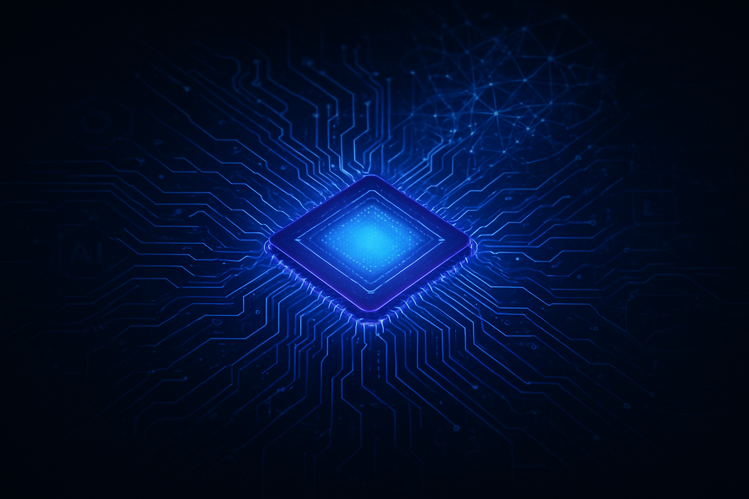
The relentless pursuit of greater computational power for artificial intelligence is driving a fundamental transformation in semiconductor manufacturing, with advanced packaging and lithography emerging as the twin pillars supporting the next era of AI innovation. As traditional silicon scaling, often referred to as Moore's Law, faces physical and economic limitations, these sophisticated technologies are not merely extending chip capabilities but are indispensable for powering the increasingly complex demands of modern AI, from colossal large language models to pervasive edge computing. Their immediate significance lies in enabling unprecedented levels of performance, efficiency, and integration, fundamentally reshaping the design and production of AI-specific hardware and intensifying the strategic competition within the global tech industry.
Innovations and Limitations: The Core of AI Semiconductor Evolution
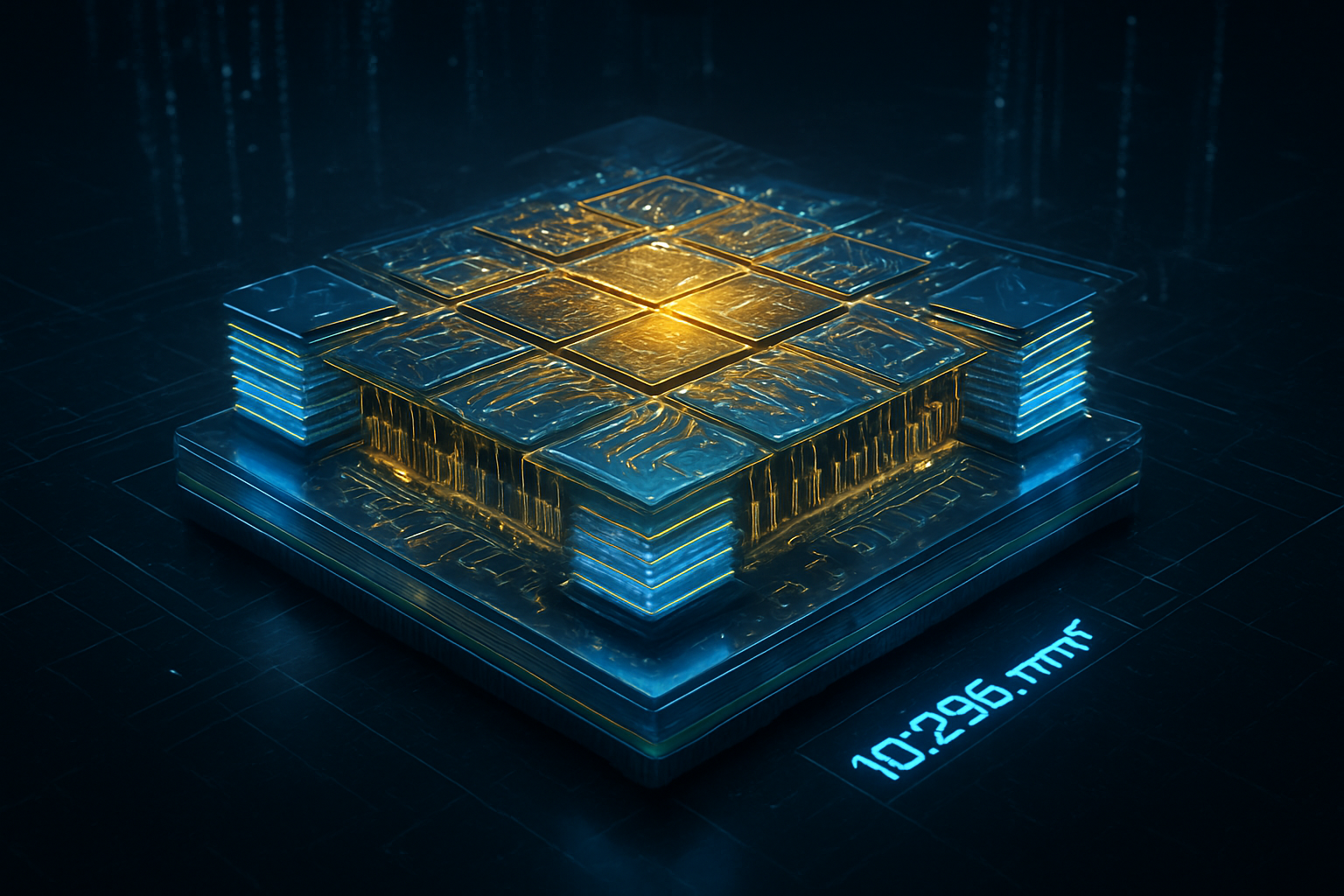
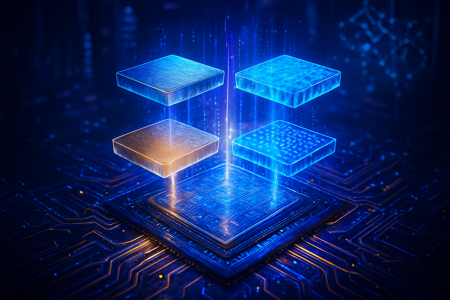
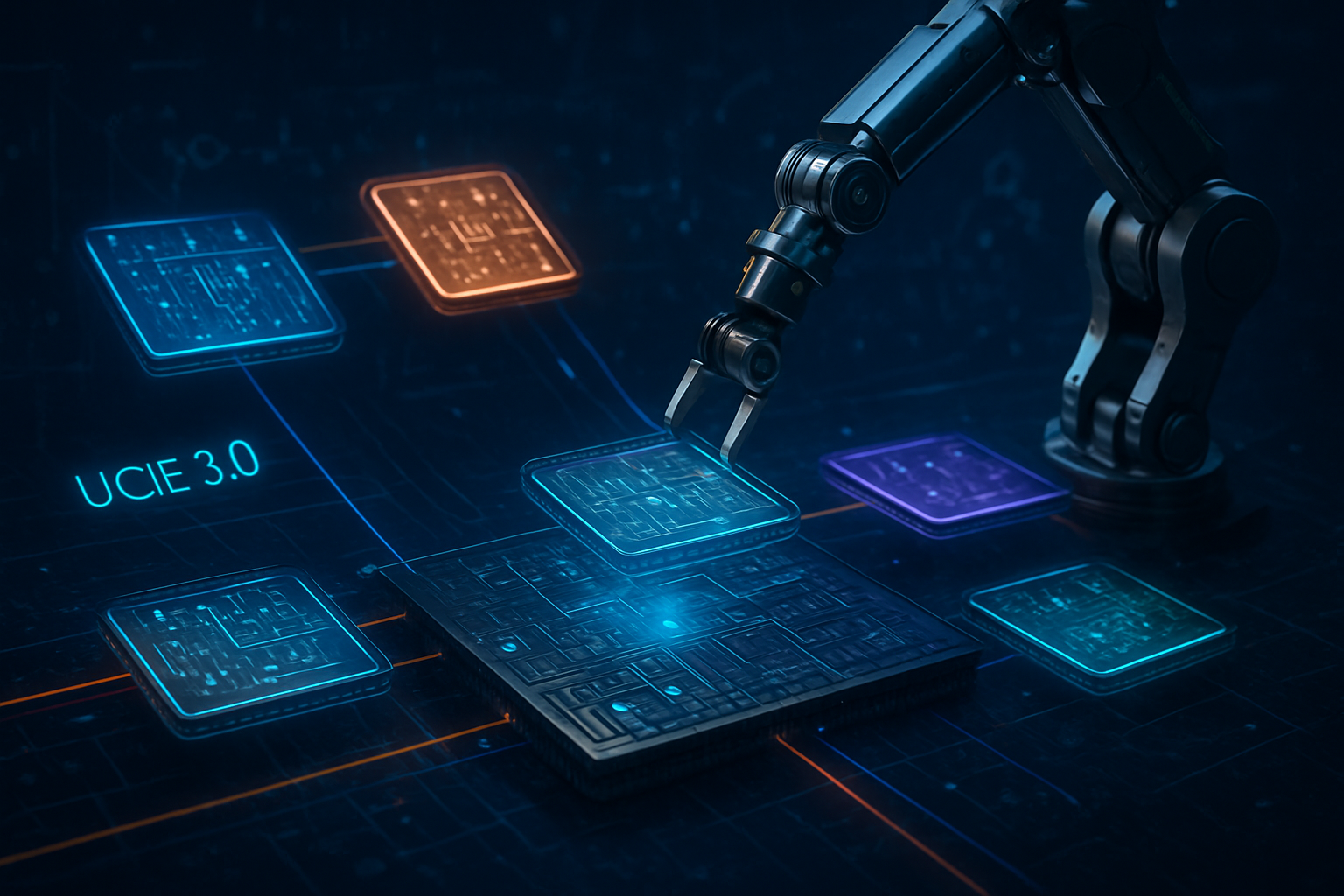
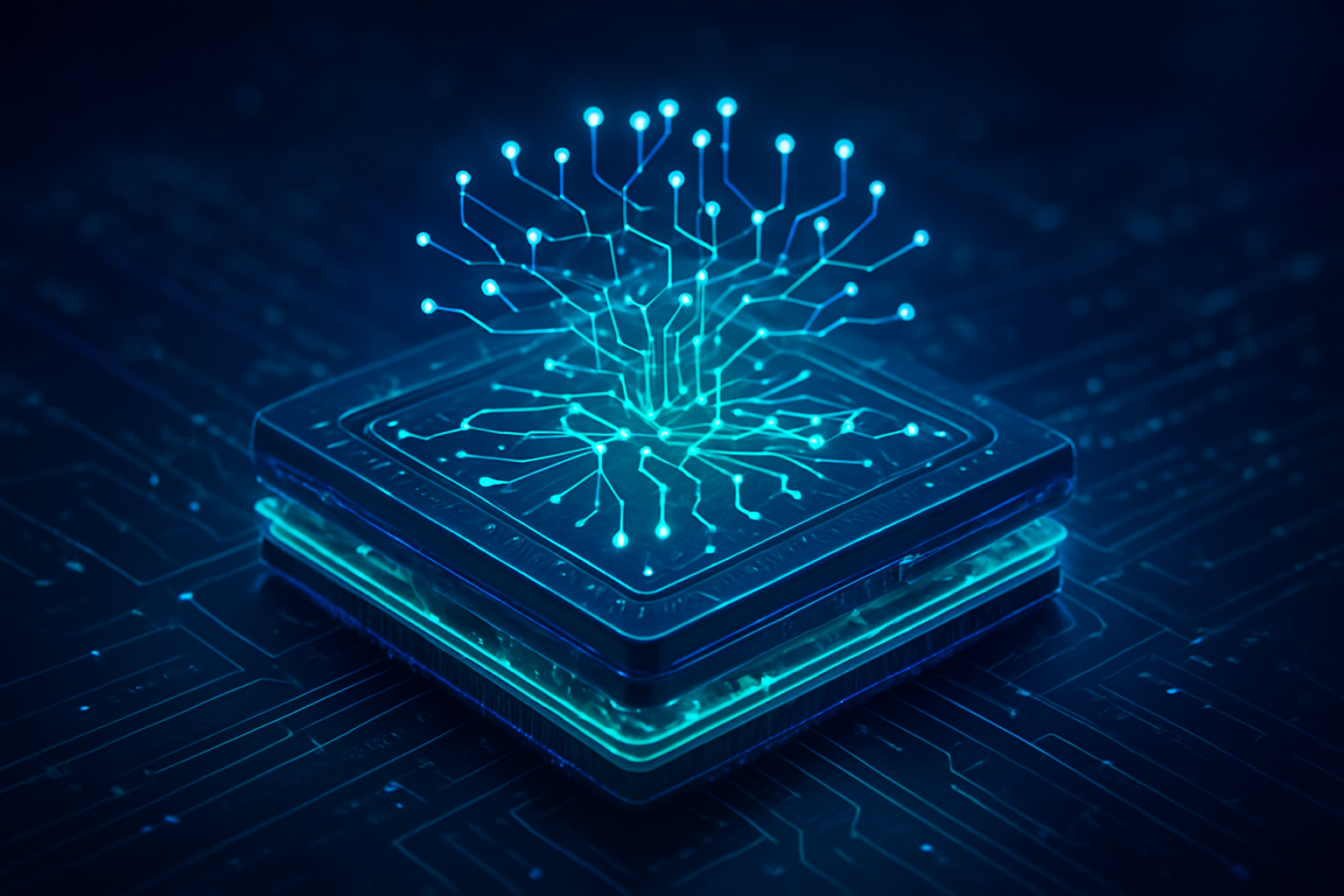
The AI semiconductor landscape is currently defined by a furious pace of innovation in both advanced packaging and lithography, each addressing critical bottlenecks while simultaneously presenting new challenges. In advanced packaging, the shift towards heterogeneous integration is paramount. Technologies such as 2.5D and 3D stacking, exemplified by Taiwan Semiconductor Manufacturing Company (TSMC) (TPE: 2330)'s CoWoS (Chip-on-Wafer-on-Substrate) variants, allow for the precise placement of multiple dies—including high-bandwidth memory (HBM) and specialized AI accelerators—on a single interposer or stacked vertically. This architecture dramatically reduces data transfer distances, alleviating the "memory wall" bottleneck that has traditionally hampered AI performance by ensuring ultra-fast communication between processing units and memory. Chiplet designs further enhance this modularity, enabling optimized cost and performance by allowing different components to be fabricated on their most suitable process nodes and improving manufacturing yields. Innovations like Intel Corporation (NASDAQ: INTC)'s EMIB (Embedded Multi-die Interconnect Bridge) and emerging Co-Packaged Optics (CPO) for AI networking are pushing the boundaries of integration, promising significant gains in efficiency and bandwidth by the late 2020s.
However, these advancements come with inherent limitations. The complexity of integrating diverse materials and components in 2.5D and 3D packages introduces significant thermal management challenges, as denser integration generates more heat. The precise alignment required for vertical stacking demands incredibly tight tolerances, increasing manufacturing complexity and potential for defects. Yield management for these multi-die assemblies is also more intricate than for monolithic chips. Initial reactions from the AI research community and industry experts highlight these trade-offs, recognizing the immense performance gains but also emphasizing the need for robust thermal solutions, advanced testing methodologies, and more sophisticated design automation tools to fully realize the potential of these packaging innovations.
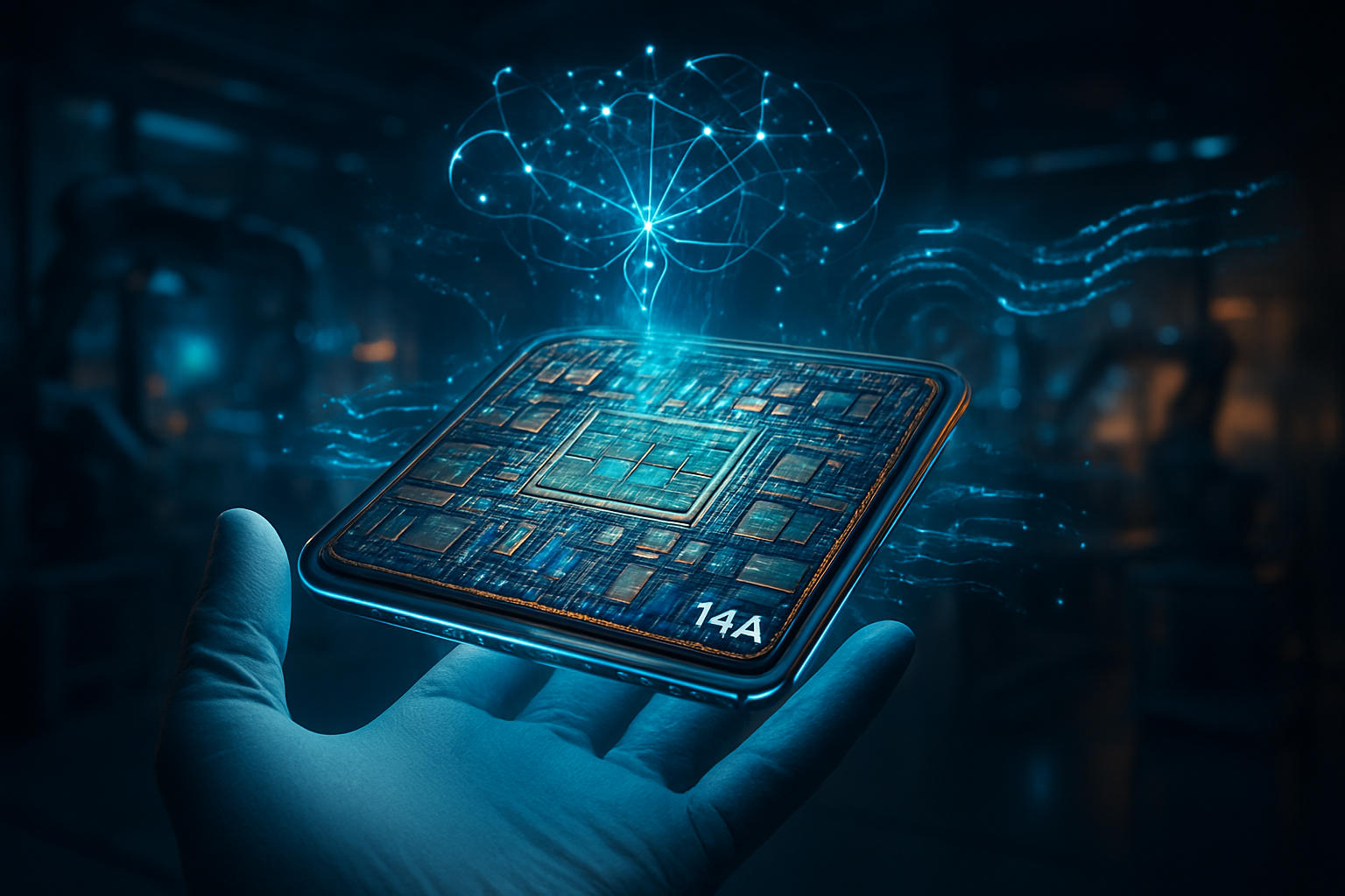
Concurrently, lithography continues its relentless march towards finer features, with Extreme Ultraviolet (EUV) lithography at the forefront. EUV, utilizing 13.5nm wavelength light, enables the fabrication of transistors at 7nm, 5nm, 3nm, and even smaller nodes, which are absolutely critical for the density and efficiency required by modern AI processors. ASML Holding N.V. (NASDAQ: ASML) remains the undisputed leader, holding a near-monopoly on these highly complex and expensive machines. The next frontier is High-NA EUV, with a larger numerical aperture lens (0.55), promising to push feature sizes below 10nm, crucial for future 2nm and 1.4nm nodes like TSMC's A14 process, expected around 2027. While Deep Ultraviolet (DUV) lithography still plays a vital role for less critical layers and memory, the push for leading-edge AI chips is entirely dependent on EUV and its subsequent generations.
The limitations in lithography primarily revolve around cost, complexity, and the fundamental physics of light. High-NA EUV systems, for instance, are projected to cost around $384 million each, making them an enormous capital expenditure for chip manufacturers. The extreme precision required, the specialized mask infrastructure, and the challenges of defect control at such minuscule scales contribute to significant manufacturing hurdles and impact overall yields. Emerging technologies like X-ray lithography (XRL) and nanoimprint lithography are being explored as potential long-term solutions to overcome some of these inherent limitations and to avoid the need for costly multi-patterning techniques at future nodes. Furthermore, AI itself is increasingly being leveraged within lithography processes, optimizing mask designs, predicting defects, and refining process parameters to improve efficiency and yield, demonstrating a symbiotic relationship between AI development and the tools that enable it.
The Shifting Sands of AI Supremacy: Who Benefits from the Packaging and Lithography Revolution
The advancements in advanced packaging and lithography are not merely technical feats; they are profound strategic enablers, fundamentally reshaping the competitive landscape for AI companies, tech giants, and burgeoning startups alike. At the forefront of benefiting are the major semiconductor foundries and Integrated Device Manufacturers (IDMs) like Taiwan Semiconductor Manufacturing Company (TSMC) (TPE: 2330), Intel Corporation (NASDAQ: INTC), and Samsung Electronics Co., Ltd. (KRX: 005930). TSMC's dominance in advanced packaging technologies such as CoWoS and InFO makes it an indispensable partner for virtually all leading AI chip designers. Similarly, Intel's EMIB and Foveros, and Samsung's I-Cube, are critical offerings that allow these giants to integrate diverse components into high-performance packages, solidifying their positions as foundational players in the AI supply chain. Their massive investments in expanding advanced packaging capacity underscore its strategic importance.
AI chip designers and accelerator developers are also significant beneficiaries. NVIDIA Corporation (NASDAQ: NVDA), the undisputed leader in AI GPUs, heavily leverages 2.5D and 3D stacking with High Bandwidth Memory (HBM) for its cutting-edge accelerators like the H100, maintaining its competitive edge. Advanced Micro Devices, Inc. (NASDAQ: AMD) is a strong challenger, utilizing similar packaging strategies for its MI300 series. Hyperscalers and tech giants like Alphabet Inc. (Google) (NASDAQ: GOOGL) with its TPUs and Amazon.com, Inc. (NASDAQ: AMZN) with its Graviton and Trainium chips are increasingly relying on custom silicon, optimized through advanced packaging, to achieve superior performance-per-watt and cost efficiency for their vast AI workloads. This trend signals a broader move towards vertical integration where software, silicon, and packaging are co-designed for maximum impact.
The competitive implications are stark. Advanced packaging has transcended its traditional role as a back-end process to become a core architectural enabler and a strategic differentiator. Companies with robust R&D and manufacturing capabilities in these areas gain substantial advantages, while those lagging risk being outmaneuvered. The shift towards modular, chiplet-based architectures, facilitated by advanced packaging, is a significant disruption. It allows for greater flexibility and could, to some extent, democratize chip design by enabling smaller startups to innovate by integrating specialized chiplets without the prohibitively high cost of designing an entire System-on-a-Chip (SoC) from scratch. However, this also introduces new challenges around chiplet interoperability and standardization. The "memory wall" – the bottleneck in data transfer between processing units and memory – is directly addressed by advanced packaging, which is crucial for the performance of large language models and generative AI.
Market positioning is increasingly defined by access to and expertise in these advanced technologies. ASML Holding N.V. (NASDAQ: ASML), as the sole provider of leading-edge EUV lithography systems, holds an unparalleled strategic advantage, making it one of the most critical companies in the entire semiconductor ecosystem. Memory manufacturers like SK Hynix Inc. (KRX: 000660), Micron Technology, Inc. (NASDAQ: MU), and Samsung are experiencing surging demand for HBM, essential for high-performance AI accelerators. Outsourced Semiconductor Assembly and Test (OSAT) providers such as ASE Technology Holding Co., Ltd. (NYSE: ASX) and Amkor Technology, Inc. (NASDAQ: AMKR) are also becoming indispensable partners in the complex assembly of these advanced packages. Ultimately, the ability to rapidly innovate and scale production of AI chips through advanced packaging and lithography is now a direct determinant of strategic advantage and market leadership in the fiercely competitive AI race.
A New Foundation for AI: Broader Implications and Looming Concerns
The current revolution in advanced packaging and lithography is far more than an incremental improvement; it represents a foundational shift that is profoundly impacting the broader AI landscape and shaping its future trajectory. These hardware innovations are the essential bedrock upon which the next generation of AI systems, particularly the resource-intensive large language models (LLMs) and generative AI, are being built. By enabling unprecedented levels of performance, efficiency, and integration, they allow for the realization of increasingly complex neural network architectures and greater computational density, pushing the boundaries of what AI can achieve. This scaling is critical for everything from hyperscale data centers powering global AI services to compact, energy-efficient AI at the edge in devices and autonomous systems.
This era of hardware innovation fits into the broader AI trend of moving beyond purely algorithmic breakthroughs to a symbiotic relationship between software and silicon. While previous AI milestones, such as the advent of deep learning algorithms or the widespread adoption of GPUs for parallel processing, were primarily driven by software and architectural insights, advanced packaging and lithography provide the physical infrastructure necessary to scale and deploy these innovations efficiently. They are directly addressing the "memory wall" bottleneck, a long-standing limitation in AI accelerator performance, by placing memory closer to processing units, leading to faster data access, higher bandwidth, and lower latency—all critical for the data-hungry demands of modern AI. This marks a departure from reliance solely on Moore's Law, as packaging has transitioned from a supportive back-end process to a core architectural enabler, integrating diverse chiplets and components into sophisticated "mini-systems."
However, this transformative period is not without its concerns. The primary challenges revolve around the escalating cost and complexity of these advanced manufacturing processes. Designing, manufacturing, and testing 2.5D/3D stacked chips and chiplet systems are significantly more complex and expensive than traditional monolithic designs, leading to increased development costs and longer design cycles. The exorbitant price of High-NA EUV tools, for instance, translates into higher wafer costs. Thermal management is another critical issue; denser integration in advanced packages generates more localized heat, demanding innovative and robust cooling solutions to prevent performance degradation and ensure reliability.
Perhaps the most pressing concern is the bottleneck in advanced packaging capacity. Technologies like TSMC's CoWoS are in such high demand that hyperscalers are pre-booking capacity up to eighteen months in advance, leaving smaller startups struggling to secure scarce slots and often facing idle wafers awaiting packaging. This capacity crunch can stifle innovation and slow the deployment of new AI technologies. Furthermore, geopolitical implications are significant, with export restrictions on advanced lithography machines to certain countries (e.g., China) creating substantial tensions and impacting their ability to produce cutting-edge AI chips. The environmental impact also looms large, as these advanced manufacturing processes become more energy-intensive and resource-demanding. Some experts even predict that the escalating demand for AI training could, in a decade or so, lead to power consumption exceeding globally available power, underscoring the urgent need for even more efficient models and hardware.
The Horizon of AI Hardware: Future Developments and Expert Predictions
The trajectory of advanced packaging and lithography points towards an even more integrated and specialized future for AI semiconductors. In the near-term, we can expect a continued rapid expansion of 2.5D and 3D integration, with a focus on improving hybrid bonding techniques to achieve even finer interconnect pitches and higher stack densities. The widespread adoption of chiplet architectures will accelerate, driven by the need for modularity, cost-effectiveness, and the ability to mix-and-match specialized components from different process nodes. This will necessitate greater standardization in chiplet interfaces and communication protocols to foster a more open and interoperable ecosystem. The commercialization and broader deployment of High-NA EUV lithography, particularly for sub-2nm process nodes, will be a critical near-term development, enabling the next generation of ultra-dense transistors.
Looking further ahead, long-term developments include the exploration of novel materials and entirely new integration paradigms. Co-Packaged Optics (CPO) will likely become more prevalent, integrating optical interconnects directly into advanced packages to overcome electrical bandwidth limitations for inter-chip and inter-system communication, crucial for exascale AI systems. Experts predict the emergence of "system-on-wafer" or "system-in-package" solutions that blur the lines between chip and system, creating highly integrated, application-specific AI engines. Research into alternative lithography methods like X-ray lithography and nanoimprint lithography could offer pathways beyond the physical limits of current EUV technology, potentially enabling even finer features without the complexities of multi-patterning.
The potential applications and use cases on the horizon are vast. More powerful and efficient AI chips will enable truly ubiquitous AI, powering highly autonomous vehicles with real-time decision-making capabilities, advanced personalized medicine through rapid genomic analysis, and sophisticated real-time simulation and digital twin technologies. Generative AI models will become even larger and more capable, moving beyond text and images to create entire virtual worlds and complex interactive experiences. Edge AI devices, from smart sensors to robotics, will gain unprecedented processing power, enabling complex AI tasks locally without constant cloud connectivity, enhancing privacy and reducing latency.
However, several challenges need to be addressed to fully realize this future. Beyond the aforementioned cost and thermal management issues, the industry must tackle the growing complexity of design and verification for these highly integrated systems. New Electronic Design Automation (EDA) tools and methodologies will be essential. Supply chain resilience and diversification will remain critical, especially given geopolitical tensions. Furthermore, the energy consumption of AI training and inference, already a concern, will demand continued innovation in energy-efficient hardware architectures and algorithms to ensure sustainability. Experts predict a future where hardware and software co-design becomes even more intertwined, with AI itself playing a crucial role in optimizing chip design, manufacturing processes, and even material discovery. The industry is moving towards a holistic approach where every layer of the technology stack, from atoms to algorithms, is optimized for AI.
The Indispensable Foundation: A Wrap-up on AI's Hardware Revolution
The advancements in advanced packaging and lithography are not merely technical footnotes in the story of AI; they are the bedrock upon which the future of artificial intelligence is being constructed. The key takeaway is clear: as traditional methods of scaling transistor density reach their physical and economic limits, these sophisticated hardware innovations have become indispensable for continuing the exponential growth in computational power required by modern AI. They are enabling heterogeneous integration, alleviating the "memory wall" with High Bandwidth Memory, and pushing the boundaries of miniaturization with Extreme Ultraviolet lithography, thereby unlocking unprecedented performance and efficiency for everything from generative AI to edge computing.
This development marks a pivotal moment in AI history, akin to the introduction of the GPU for parallel processing or the breakthroughs in deep learning algorithms. Unlike those milestones, which were largely software or architectural, advanced packaging and lithography provide the fundamental physical infrastructure that allows these algorithmic and architectural innovations to be realized at scale. They represent a strategic shift where the "back-end" of chip manufacturing has become a "front-end" differentiator, profoundly impacting competitive dynamics among tech giants, fostering new opportunities for innovation, and presenting significant challenges related to cost, complexity, and supply chain bottlenecks.
The long-term impact will be a world increasingly permeated by intelligent systems, powered by chips that are more integrated, specialized, and efficient than ever before. This hardware revolution will enable AI to tackle problems of greater complexity, operate with higher autonomy, and integrate seamlessly into every facet of our lives. In the coming weeks and months, we should watch for continued announcements regarding expanded advanced packaging capacity from leading foundries, further refinements in High-NA EUV deployment, and the emergence of new chiplet standards. The race for AI supremacy will increasingly be fought not just in algorithms and data, but in the very atoms and architectures that form the foundation of intelligent machines.
This content is intended for informational purposes only and represents analysis of current AI developments.
TokenRing AI delivers enterprise-grade solutions for multi-agent AI workflow orchestration, AI-powered development tools, and seamless remote collaboration platforms.
For more information, visit https://www.tokenring.ai/.