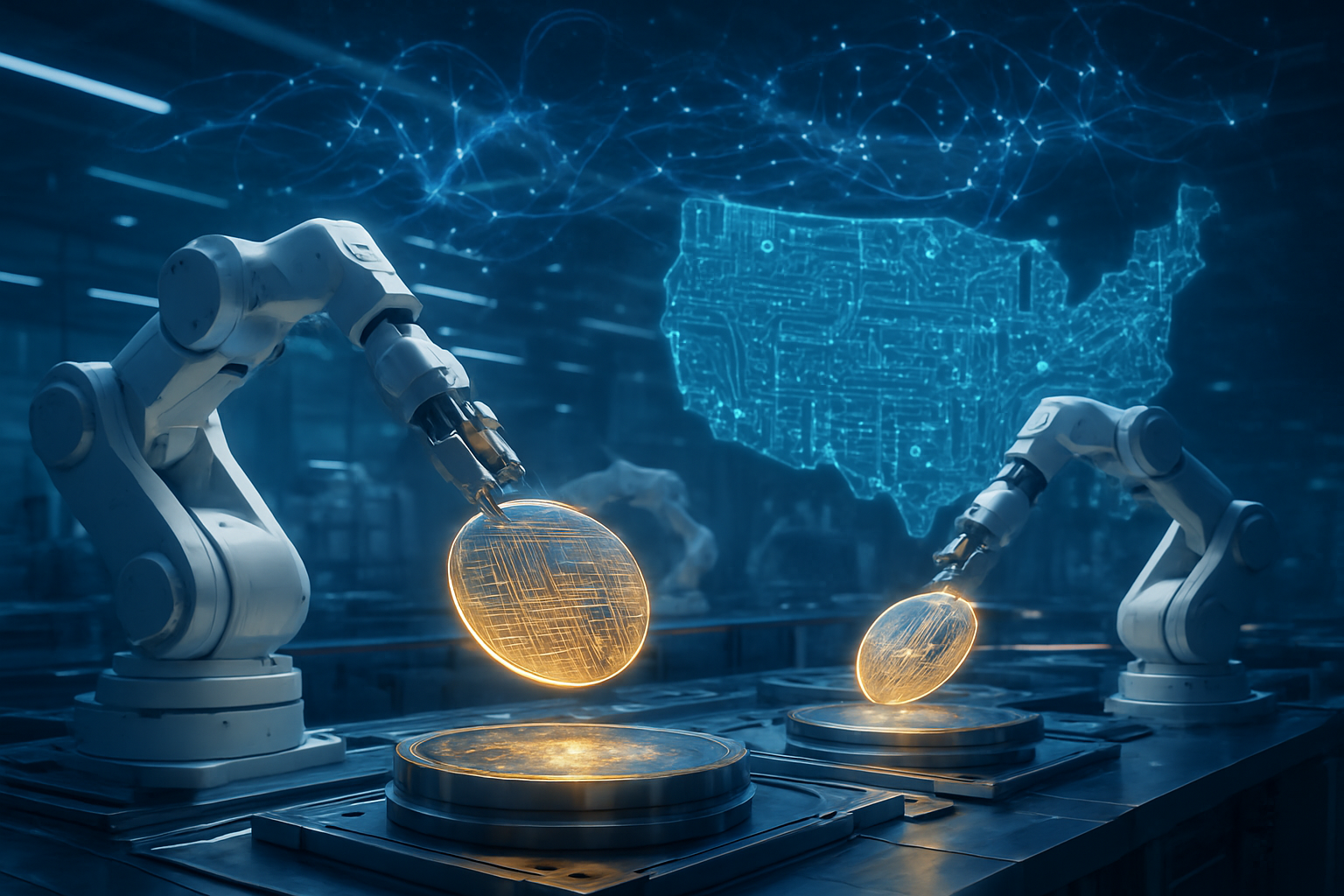
Tag: CHIPS Act

  • Micron’s $100 Billion New York Megafab: A Catalyst for U.S. Semiconductor Dominance and AI Innovation

    CLAY, NY – December 16, 2025 – In a monumental stride towards fortifying America's technological independence and securing its future in the global semiconductor landscape, Micron Technology (NASDAQ: MU) announced its plans on October 4, 2022, to construct a colossal new semiconductor megafab in Clay, New York. This ambitious project, projected to involve an investment of up to $100 billion over the next two decades, represents the largest private investment in New York state history and a critical pillar in the nation's strategy to re-shore advanced manufacturing. The megafab is poised to significantly bolster domestic production of leading-edge memory, specifically DRAM, and is a direct outcome of the bipartisan CHIPS and Science Act, underscoring a concerted effort to create a more resilient, secure, and geographically diverse semiconductor supply chain.

    The immediate significance of this endeavor cannot be overstated. By aiming to ramp up U.S.-based DRAM production to 40% of its global output within the next decade, Micron is not merely building a factory; it is laying the groundwork for a revitalized domestic manufacturing ecosystem. This strategic move is designed to mitigate vulnerabilities exposed by recent global supply chain disruptions, ensuring a stable and secure source of the advanced memory vital for everything from artificial intelligence and electric vehicles to 5G technology and national defense. The "Made in New York" microchips emerging from this facility will be instrumental in powering the next generation of technological innovation, strengthening both U.S. economic and national security.

    Engineering a New Era: Technical Prowess and Strategic Imperatives

    Micron's New York megafab is set to be a beacon of advanced semiconductor manufacturing, pushing the boundaries of what's possible in memory production. The facility will be equipped with state-of-the-art tools and processes, including the sophisticated extreme ultraviolet (EUV) lithography. This cutting-edge technology is crucial for producing the most advanced DRAM nodes, allowing for the creation of smaller, more powerful, and energy-efficient memory chips. Unlike older fabrication plants that rely on less precise deep ultraviolet (DUV) lithography, EUV enables higher transistor density and improved performance, critical for the demanding requirements of modern computing, especially in AI and high-performance computing (HPC) applications.

    This strategic investment marks a significant departure from the decades-long trend of outsourcing semiconductor manufacturing to East Asia. For years, the U.S. share of global semiconductor manufacturing capacity has dwindled, raising concerns about economic competitiveness and national security. Micron's megafab, alongside other CHIPS Act-supported initiatives, directly addresses this by bringing leading-edge process technology back to American soil. The facility is expected to drive industry leadership across multiple generations of DRAM, ensuring that the U.S. remains at the forefront of memory innovation. Initial reactions from the AI research community and industry experts have been overwhelmingly positive, highlighting the critical need for a diversified and secure supply of advanced memory to sustain the rapid pace of AI development and deployment. The ability to access domestically produced, high-performance DRAM will accelerate research, reduce time-to-market for AI products, and foster greater collaboration between chip manufacturers and AI developers.

    Reshaping the AI Landscape: Beneficiaries and Competitive Dynamics

    The implications of Micron's New York megafab for AI companies, tech giants, and startups are profound and far-reaching. Companies heavily reliant on advanced memory, such as NVIDIA (NASDAQ: NVDA), Google (NASDAQ: GOOGL), Amazon (NASDAQ: AMZN), and Microsoft (NASDAQ: MSFT), which power their AI models and cloud infrastructure with vast arrays of GPUs and high-bandwidth memory (HBM), stand to benefit immensely. A more secure, stable, and potentially faster supply of cutting-edge DRAM and future HBM variants from a domestic source will de-risk their supply chains, reduce lead times, and potentially even lower costs in the long run. This stability is crucial for the continuous innovation cycle in AI, where new models and applications constantly demand more powerful and efficient memory solutions.

    The competitive landscape for major AI labs and tech companies will also be subtly, yet significantly, altered. While the megafab won't directly produce AI accelerators, its output is the lifeblood of these systems. Companies with direct access or preferential agreements for domestically produced memory could gain a strategic advantage, ensuring they have the necessary components to scale their AI operations and deploy new services faster than competitors. This could lead to a competitive shift, favoring those who can leverage a more resilient domestic supply chain. Potential disruption to existing products or services is less about direct competition and more about enablement: a more robust memory supply could accelerate the development of entirely new AI applications that were previously constrained by memory availability or cost. For startups, this could mean easier access to the foundational components needed to innovate, fostering a vibrant ecosystem of AI-driven ventures.

    A Cornerstone in the Broader AI and Geopolitical Tapestry

    Micron's megafab in New York is not just a factory; it's a strategic national asset that fits squarely into the broader AI landscape and global geopolitical trends. It represents a tangible commitment to strengthening the U.S. position in the critical technology race against rivals, particularly China. By bringing leading-edge memory manufacturing back home, the U.S. enhances its national security posture, reducing reliance on potentially vulnerable foreign supply chains for components essential to defense, intelligence, and critical infrastructure. This move is a powerful statement about the importance of technological sovereignty and economic resilience in an increasingly complex world.

    The impacts extend beyond security to economic revitalization. The project is expected to create nearly 50,000 jobs in New York—9,000 high-paying Micron jobs and over 40,000 community jobs—transforming Central New York into a major hub for the semiconductor industry. This job creation and economic stimulus are critical, demonstrating how strategic investments in advanced manufacturing can foster regional growth. Potential concerns, however, include the significant demand for skilled labor, the environmental impact of such a large industrial facility, and the need for robust infrastructure development to support it. Comparisons to previous AI milestones, such as the development of foundational large language models or the breakthroughs in deep learning, highlight that while AI algorithms and software are crucial, their ultimate performance and scalability are intrinsically linked to the underlying hardware. Without advanced memory, the most sophisticated AI models would remain theoretical constructs.

    Charting the Future: Applications and Challenges Ahead

    Looking ahead, the Micron megafab promises a cascade of near-term and long-term developments. In the near term, we can expect a gradual ramp-up of construction and equipment installation, followed by initial production of advanced DRAM. This will likely be accompanied by a surge in local training programs and educational initiatives to cultivate the skilled workforce required for such a sophisticated operation. Long-term, the facility will become a cornerstone for future memory innovation, potentially leading to the development and mass production of next-generation memory technologies crucial for advanced AI, quantum computing, and neuromorphic computing architectures.

    The potential applications and use cases on the horizon are vast. Domestically produced advanced DRAM will fuel the expansion of AI data centers, enable more powerful edge AI devices, accelerate autonomous driving technologies, and enhance capabilities in fields like medical imaging and scientific research. It will also be critical for defense applications, ensuring secure and high-performance computing for military systems. Challenges that need to be addressed include attracting and retaining top talent in a competitive global market, managing the environmental footprint of the facility, and ensuring a continuous pipeline of innovation to maintain technological leadership. Experts predict that this investment will not only solidify the U.S. position in memory manufacturing but also catalyze further investments across the entire semiconductor supply chain, from materials to packaging, creating a more robust and self-sufficient domestic industry.

    A Defining Moment for American Tech

    Micron's $100 billion megafab in New York represents a defining moment for American technology and industrial policy. The key takeaway is a clear commitment to re-establishing U.S. leadership in semiconductor manufacturing, particularly in the critical domain of advanced memory. This development is not merely about building a factory; it's about building resilience, fostering innovation, and securing the foundational components necessary for the next wave of AI breakthroughs. Its significance in AI history will be seen as a crucial step in ensuring that the hardware infrastructure can keep pace with the accelerating demands of AI software.

    Final thoughts underscore the long-term impact: this megafab will serve as a powerful engine for economic growth, job creation, and national security for decades to come. It positions the U.S. to be a more reliable and independent player in the global technology arena. In the coming weeks and months, observers will be watching for updates on construction progress, hiring initiatives, and any further announcements regarding partnerships or technological advancements at the site. The successful realization of this megafab's full potential will be a testament to the power of strategic industrial policy and a harbinger of a more secure and innovative future for American AI.


    This content is intended for informational purposes only and represents analysis of current AI developments.

    TokenRing AI delivers enterprise-grade solutions for multi-agent AI workflow orchestration, AI-powered development tools, and seamless remote collaboration platforms.
    For more information, visit https://www.tokenring.ai/.

  • America’s Chip Gambit: The CHIPS Act Ignites a New Era of Domestic Semiconductor Production

    America’s Chip Gambit: The CHIPS Act Ignites a New Era of Domestic Semiconductor Production

    Washington D.C., December 12, 2025 – In a bold strategic move to reclaim global leadership in advanced technology and fortify critical supply chains, the United States has embarked on an ambitious journey to revitalize its domestic semiconductor manufacturing capabilities. The Creating Helpful Incentives to Produce Semiconductors (CHIPS) and Science Act of 2022, signed into law on August 9, 2022, stands as the cornerstone of this national endeavor. This landmark legislation, allocating approximately $280 billion, is designed to reverse decades of manufacturing decline, reduce perilous reliance on foreign chip production, and usher in a new era of American technological self-sufficiency.

    The immediate significance of the CHIPS Act cannot be overstated. It has acted as a powerful catalyst, spurring an unprecedented wave of private investment and project announcements across the nation. With substantial financial incentives, including grants, loans, and a crucial investment tax credit, the Act has transformed the landscape for semiconductor companies, prompting major players to commit billions to establish and expand advanced manufacturing facilities within U.S. borders. This concerted effort aims not only to secure the nation's economic future but also to safeguard its national security interests in an increasingly complex geopolitical environment.

    A Deep Dive into the CHIPS Act and Global Strategies

    The CHIPS Act represents a monumental shift in U.S. industrial policy, directly addressing the precipitous decline in America's share of global semiconductor manufacturing, which plummeted from 37% in 1990 to a mere 12% by 2020. At its core, the Act allocates approximately $52.7 billion specifically for semiconductor manufacturing, research and development (R&D), and workforce training. Of this, a substantial $39 billion is earmarked for direct financial incentives—grants, cooperative agreements, and loan guarantees—to companies that build, expand, or modernize semiconductor fabrication facilities (fabs) in the United States. Furthermore, a critical 25% investment tax credit for manufacturing equipment costs provides an additional, long-term incentive for capital-intensive projects. This comprehensive financial package is a stark departure from the largely hands-off approach of previous decades, signaling a proactive government role in strategic industries.

    The technical specifications of the CHIPS Act are designed to attract the most advanced manufacturing processes. Incentives are heavily weighted towards leading-edge logic and memory chip production, which are crucial for artificial intelligence, high-performance computing, and defense applications. Companies like Intel (NASDAQ: INTC), Taiwan Semiconductor Manufacturing Company (TSMC) (NYSE: TSM), and Samsung (KRX: 005930) have already committed to multi-billion-dollar investments, receiving or expecting significant federal support. For instance, Intel has been allocated $8.5 billion for projects across Arizona, New Mexico, Oregon, and Ohio, while TSMC and Samsung have received $6.6 billion and $6.4 billion, respectively, to bolster their U.S. manufacturing footprint. This targeted approach differs significantly from earlier, broader industrial policies by focusing on a specific, high-tech sector deemed vital for national security and economic competitiveness.

    Initial reactions from the AI research community and industry experts have been largely positive, albeit with some caveats. There is widespread agreement that strengthening domestic semiconductor supply chains is essential for innovation in AI, as access to cutting-edge chips is paramount for developing and deploying advanced AI models. However, some experts caution that the sheer scale and complexity of building a robust semiconductor ecosystem mean that the full benefits will take years, if not decades, to materialize. Concerns have also been raised about the potential for market distortions and the challenge of cultivating a sufficiently skilled workforce at the pace required by these ambitious projects.

    Comparing the CHIPS Act to national strategies reveals a global trend towards industrial policy in semiconductors. The European Union has launched its own "European Chips Act," aiming to double its share of global chip production to 20% by 2030, backed by €43 billion in public and private investment. Japan and South Korea have also introduced significant subsidy programs and tax incentives to attract and retain semiconductor manufacturing. While the U.S. CHIPS Act emphasizes national security and technological leadership, the EU's approach also prioritizes digital sovereignty and environmental sustainability. Japan's strategy often involves attracting foreign direct investment from leading foundries, while South Korea focuses on bolstering its existing domestic champions like Samsung and SK Hynix (KRX: 000660). The effectiveness of these strategies will depend on sustained political will, efficient allocation of funds, and the ability to attract and retain top talent in a highly competitive global market. The U.S. approach, with its substantial financial firepower and focus on leading-edge technology, appears to be rapidly gaining traction and attracting significant private sector commitments, positioning it as one of the most aggressive and potentially impactful national strategies to date.

    Reshaping the Competitive Landscape: Winners and Disruptors in the Chip Renaissance

    The CHIPS Act and its global counterparts are fundamentally redrawing the competitive map for both semiconductor manufacturers and the burgeoning AI industry. Direct beneficiaries of the U.S. legislation include a roster of industry giants and specialized players. Intel (NASDAQ: INTC) stands out as a primary recipient, securing $8.5 billion in grants and $11 billion in loans to fuel its ambitious $100 billion investment in new fabs in Arizona and Ohio, alongside expansions in Oregon and New Mexico. This massive infusion is critical for Intel's resurgence in process technology, aiming to regain leadership with its cutting-edge Intel 18A node. Similarly, Taiwan Semiconductor Manufacturing Company (TSMC) (NYSE: TSM), the world's leading contract chipmaker, has been allocated $6.6 billion to establish three advanced fabs in Arizona, representing a staggering $65 billion investment and ensuring a robust domestic supply of 4nm, 3nm, and 2nm chips for U.S. tech titans. Samsung (KRX: 005930) and Micron Technology (NASDAQ: MU) have also received significant grants, $6.4 billion and $6.1 billion respectively, to bolster their U.S. manufacturing capabilities in logic and memory chips.

    For major AI labs and tech companies, the competitive implications are profound. Guaranteed access to advanced semiconductor hardware is becoming as critical as software innovation itself. AI development, particularly for training large language models and other complex neural networks, is insatiably hungry for the latest GPUs and specialized AI accelerators. A stable, resilient domestic supply of these chips, fostered by the CHIPS Act, directly mitigates the risk of supply chain disruptions that can cripple research and delay product launches. Companies with robust supply chains, in-house chip design capabilities (like Apple's (NASDAQ: AAPL) M-series chips), or strategic partnerships with foundries will gain a distinct advantage, potentially leading to a consolidation of advanced AI development around well-resourced players.

    The potential for disruption to existing products and services is multifaceted. While the primary aim is to enhance supply chain resilience and prevent future shortages—a significant disruption experienced during the pandemic across sectors from automotive to consumer electronics—the accelerated development of next-generation chips could also spur entirely new product categories or significantly enhance existing ones. Companies that fail to adapt their sourcing strategies or invest in design flexibility might face delays or be forced to redesign products with less optimal components. Conversely, increased domestic production is projected to shorten lead times for chips by up to 30%, offering manufacturers better inventory management and greater agility in bringing new innovations to market.

    Strategically, companies that can demonstrate secure and resilient supply chains will gain a significant market positioning advantage, fostering greater customer loyalty and reducing geopolitical risks. The establishment of new domestic innovation hubs, such as the U.S. National Semiconductor Technology Center (NSTC), will also foster closer collaboration between industry, academia, and government, accelerating R&D. However, companies receiving CHIPS Act funding face restrictions, particularly concerning expanding advanced manufacturing operations in countries deemed a national security threat. This underscores a broader geopolitical reorientation, where technological self-sufficiency and reduced reliance on specific foreign nations are paramount, pushing companies to re-evaluate their global manufacturing and supply chain strategies.

    A New Geopolitical Chessboard: AI, Chips, and the Global Power Struggle

    The CHIPS Act and parallel global initiatives are not merely economic policies; they are strategic maneuvers that profoundly reconfigure the broader AI landscape and global geopolitical dynamics. The current era of AI, dominated by the insatiable computational demands of large language models (LLMs) and generative AI, has elevated advanced semiconductors from mere components to the very bedrock of technological supremacy. These governmental interventions signal a global recognition that continued AI advancement is inextricably linked to a stable, secure, and cutting-edge semiconductor supply chain. This strategic focus on hardware infrastructure represents a significant trend, emphasizing that the ability to design, manufacture, and access advanced chips is now a prerequisite for AI leadership, pushing the physical infrastructure to the forefront alongside algorithmic innovation.

    The impacts of this strategic pivot are far-reaching. Economically, the CHIPS Act aims to revitalize the U.S. semiconductor industry, targeting an increase in the U.S. share of global manufacturing from 12% to 20% by the decade's end. This is expected to generate high-paying jobs, spur economic growth, and mitigate the supply chain vulnerabilities starkly exposed during the COVID-19 pandemic. Technologically, by ensuring a steady flow of advanced semiconductors, these acts directly accelerate AI research and development, providing the essential compute power needed for training and deploying sophisticated AI models across critical sectors such as healthcare, national defense, and autonomous systems. Moreover, direct funding allocated to AI-specific research, quantum computing, and robotics further underscores the symbiotic relationship between advanced hardware and future AI breakthroughs.

    However, this ambitious undertaking is not without its concerns. The most prominent is the exacerbation of geopolitical tensions, particularly between the U.S. and China. The CHIPS Act is explicitly designed to counter China's growing influence in semiconductors, with export controls on advanced AI chips to China aiming to prevent adversaries from accessing critical technologies. This has intensified a "tech war," with China aggressively pursuing its own self-sufficiency through initiatives like "Made in China 2025." This rivalry risks fragmenting the global semiconductor market and could lead to a less efficient, more complex supply chain for companies navigating these restrictions. Additionally, the rapid expansion of domestic manufacturing under the CHIPS Act faces significant workforce challenges, with an estimated need for an additional 100,000 engineers by 2030, posing a potential bottleneck to implementation.

    Comparing this era to previous AI milestones reveals a fundamental shift. Past AI breakthroughs often centered on algorithmic advancements—from expert systems to deep learning architectures. While algorithmic innovation remains crucial, the current "AI supercycle" explicitly recognizes hardware as a primary bottleneck. The ability to reliably produce and access advanced chips, such as High Bandwidth Memory (HBM), is now a foundational element for continued AI progress, comparable to other foundational algorithmic breakthroughs. Furthermore, the scale and targeted nature of government intervention, directly incentivizing private semiconductor manufacturing with billions of dollars, is arguably unprecedented in the context of a specific technological race, reflecting the perceived national security and economic importance of AI in a way that previous AI milestones were not. This era is defined by the direct, intense intertwining of AI, chip supply, and national power, making the geopolitical dimension central to technological advancement.

    The Road Ahead: AI, Chips, and the Future of American Innovation

    The CHIPS Act, enacted in August 2022, is not a static policy but a dynamic foundation for the next chapter of American technological leadership. In the near term, the tangible effects are already evident: over $30 billion has been committed to 23 projects across 15 states, catalyzing more than $450 billion in private investment. This is translating into the rapid construction of new fabrication plants and the expansion of existing facilities by major players like GlobalFoundries (NASDAQ: GFS) and TSMC (NYSE: TSM), creating over 115,000 manufacturing and construction jobs. This immediate surge in domestic production capacity is accompanied by a projected 25% increase in U.S. semiconductor R&D spending by 2025, accelerating the development of next-generation chips crucial for AI, 5G, and quantum computing. Concurrently, significant investments are being made in workforce development, addressing a projected talent gap of 67,000 engineers and technicians by 2030 through enhanced STEM programs, apprenticeships, and university funding.

    Looking further ahead, the long-term vision of the CHIPS Act is nothing short of transformative. The U.S. aims to increase its share of global semiconductor manufacturing from 12% to 20% by the end of the decade, with an even more ambitious target of 20-30% for the most advanced logic chips, up from virtually zero in 2022. This endeavor seeks to establish a complete and resilient end-to-end semiconductor ecosystem within the U.S., from raw materials to final packaging. By securing a steady and advanced domestic chip supply, the U.S. intends to solidify its competitive edge in AI research and development, ensuring its status as a technological powerhouse. Many of the projects initiated under the Act are slated for completion by 2033, signaling a sustained, multi-decade commitment to this strategic industry.

    The advancements spurred by the CHIPS Act will unlock unprecedented potential for AI across a multitude of sectors. A reliable domestic supply of cutting-edge semiconductors will provide the vast computational resources essential for training increasingly complex AI models and deploying them efficiently. This will fuel innovation in healthcare, enabling more powerful AI for diagnostics, drug discovery, and personalized medicine. In national defense, advanced AI will power data centers, edge computing applications, and sophisticated autonomous systems. The automotive industry will see accelerated development in autonomous vehicles and advanced driver-assistance systems (ADAS), while aerospace will benefit from AI in advanced avionics and predictive maintenance. Beyond these, high-performance computing, quantum computing, and next-generation wireless networks like 5G and beyond will all be propelled forward by this renewed focus on foundational hardware.

    However, significant challenges remain. The talent gap, particularly for skilled engineers and technicians, is a persistent hurdle. Global competition, especially from Taiwan, South Korea, and China, remains fierce, with other nations also investing heavily in their domestic chip industries. Geopolitical risks, including the vulnerability of concentrated production in regions like Taiwan and the complexities introduced by export controls to countries like China, require careful navigation. Cybersecurity of highly integrated fabs and supply chains is also a critical concern. Experts, including John Neuffer of the Semiconductor Industry Association (SIA), emphasize the Act's role in catalyzing innovation and maintaining U.S. leadership. Yet, warnings from academics like Saikat Chaudhuri and Brett House highlight the risks of potential policy reversals or broad tariffs on imported chips, which could severely harm the industry and slow AI advancement. The future will likely see a continued focus on security and control, potentially leading to tighter regulations on export-controlled AI chips, alongside efforts to streamline regulatory requirements and foster international collaboration with allied nations to diversify supply chains.

    A Strategic Imperative: Securing the Future of AI

    The CHIPS Act represents a pivotal moment in the history of American industrial policy and a critical juncture for the global AI landscape. Its enactment on August 9, 2022, marked a decisive shift from a hands-off approach to a proactive, government-led strategy aimed at rebuilding domestic semiconductor manufacturing. The key takeaway is clear: advanced semiconductors are the indispensable foundation for the future of Artificial Intelligence, and securing their production is now a strategic imperative for national security, economic competitiveness, and technological leadership.

    This development signifies a profound re-assessment of the symbiotic relationship between hardware and software in the age of AI. While past AI milestones often celebrated algorithmic breakthroughs, the current "AI supercycle" underscores that the physical infrastructure—the chips themselves—is as crucial as the code they run. The billions of dollars committed through the CHIPS Act, alongside a wave of private investment exceeding $450 billion, are not just about creating jobs; they are about establishing a resilient, cutting-edge ecosystem that can reliably power the next generation of AI innovation. The U.S. is not merely aiming to catch up but to leapfrog, moving from negligible production of advanced logic chips to a significant global share within the decade.

    The long-term impact of the CHIPS Act will be measured not only in the number of fabs built or jobs created but in its ability to foster sustained innovation, mitigate geopolitical risks, and ensure the U.S. remains at the forefront of AI development. This initiative is a clear signal that governments worldwide are recognizing the strategic importance of technology sovereignty. While challenges such as workforce shortages, intense global competition, and the complexities of geopolitical tensions persist, the groundwork laid by the CHIPS Act positions the U.S. to build a more secure and robust technological future.

    In the coming weeks and months, observers will be watching for continued progress in facility construction, further announcements of funding allocations, and the tangible results of workforce development programs. The effectiveness of these initiatives will ultimately determine whether America's bold chip gambit successfully secures its technological destiny and maintains its leadership in the rapidly evolving world of artificial intelligence.


    This content is intended for informational purposes only and represents analysis of current AI developments.

    TokenRing AI delivers enterprise-grade solutions for multi-agent AI workflow orchestration, AI-powered development tools, and seamless remote collaboration platforms.
    For more information, visit https://www.tokenring.ai/.

  • The AI-Driven Data Center Boom: Igniting a Domestic Semiconductor Manufacturing Revolution

    The AI-Driven Data Center Boom: Igniting a Domestic Semiconductor Manufacturing Revolution

    The global technology landscape is undergoing a profound transformation, with the relentless expansion of the data center industry, fueled primarily by the insatiable demands of artificial intelligence (AI) and machine learning (ML), creating an unprecedented surge in demand for advanced semiconductors. This critical synergy is not merely an economic phenomenon but a strategic imperative, driving nations worldwide to prioritize and heavily invest in domestic semiconductor manufacturing, aiming for self-sufficiency and robust supply chain resilience. As of late 2025, this interplay is reshaping industrial policies, fostering massive investments, and accelerating innovation at a scale unseen in decades.

    The exponential growth of cloud computing, digital transformation initiatives across all sectors, and the rapid deployment of generative AI applications are collectively propelling the data center market to new heights. Valued at approximately $215 billion in 2023, the market is projected to reach $450 billion by 2030, with some estimates suggesting it could nearly triple to $776 billion by 2034. This expansion, particularly in hyperscale data centers, which have seen their capacity double since 2020, necessitates a foundational shift in how critical components, especially advanced chips, are sourced and produced. The implications are clear: the future of AI and digital infrastructure hinges on a secure and robust supply of cutting-edge semiconductors, sparking a global race to onshore manufacturing capabilities.

    The Technical Core: AI's Insatiable Appetite for Advanced Silicon

    The current data center boom is fundamentally distinct from previous cycles due to the unique and demanding nature of AI workloads. Unlike traditional computing, AI, especially generative AI, requires immense computational power, high-speed data processing, and specialized memory solutions. This translates into an unprecedented demand for a specific class of advanced semiconductors:

    Graphics Processing Units (GPUs) and AI Application-Specific Integrated Circuits (ASICs): GPUs remain the cornerstone of AI infrastructure, with one leading manufacturer capturing an astounding 93% of the server GPU revenue in 2024. GPU revenue is forecasted to soar from $100 billion in 2024 to $215 billion by 2030. Concurrently, AI ASICs are rapidly gaining traction, particularly as hyperscalers like Alphabet (NASDAQ: GOOGL), Amazon (NASDAQ: AMZN), and Microsoft (NASDAQ: MSFT) develop custom silicon to optimize performance, reduce latency, and lessen their reliance on third-party manufacturers. Revenue from AI ASICs is expected to reach almost $85 billion by 2030, marking a significant shift towards proprietary hardware solutions.

    Advanced Memory Solutions: To handle the vast datasets and complex models of AI, High Bandwidth Memory (HBM) and Graphics Double Data Rate (GDDR) are crucial. HBM, in particular, is experiencing explosive growth, with revenue projected to surge by up to 70% in 2025, reaching an impressive $21 billion. These memory technologies are vital for providing the necessary throughput to keep AI accelerators fed with data.

    Networking Semiconductors: The sheer volume of data moving within and between AI-powered data centers necessitates highly advanced networking components. Ethernet switches, optical interconnects, SmartNICs, and Data Processing Units (DPUs) are all seeing accelerated development and deployment, with networking semiconductor growth projected at 13% in 2025 to overcome latency and throughput bottlenecks. Furthermore, Wide Bandgap (WBG) materials like Silicon Carbide (SiC) and Gallium Nitride (GaN) are increasingly being adopted in data center power supplies. These materials offer superior efficiency, operate at higher temperatures and voltages, and significantly reduce power loss, contributing to more energy-efficient and sustainable data center operations.

    The initial reaction from the AI research community and industry experts has been one of intense focus on hardware innovation. The limitations of current silicon architectures for increasingly complex AI models are pushing the boundaries of chip design, packaging technologies, and cooling solutions. This drive for specialized, high-performance, and energy-efficient hardware represents a significant departure from the more generalized computing needs of the past, signaling a new era of hardware-software co-design tailored specifically for AI.

    Competitive Implications and Market Dynamics

    This profound synergy between data center expansion and semiconductor demand is creating significant shifts in the competitive landscape, benefiting certain companies while posing challenges for others.

    Companies Standing to Benefit: Semiconductor manufacturing giants like NVIDIA (NASDAQ: NVDA), a dominant player in the GPU market, and Intel (NASDAQ: INTC), with its aggressive foundry expansion plans, are direct beneficiaries. Similarly, contract manufacturers like Taiwan Semiconductor Manufacturing Company (TSMC) (NYSE: TSM), though facing pressure for geographical diversification, remain critical. Hyperscale cloud providers such as Alphabet, Amazon, Microsoft, and Meta (NASDAQ: META) are investing hundreds of billions in capital expenditure (CapEx) to build out their AI infrastructure, directly fueling chip demand. These tech giants are also strategically developing their custom AI ASICs, a move that grants them greater control over performance, cost, and supply chain, potentially disrupting the market for off-the-shelf AI accelerators.

    Competitive Implications: The race to develop and deploy advanced AI chips is intensifying competition among major AI labs and tech companies. Companies with strong in-house chip design capabilities or strategic partnerships with leading foundries gain a significant competitive advantage. This push for domestic manufacturing also introduces new players and expands existing facilities, leading to increased competition in fabrication. The market positioning is increasingly defined by access to advanced fabrication capabilities and a resilient supply chain, making geopolitical stability and national industrial policies critical factors.

    Potential Disruption: The trend towards custom silicon by hyperscalers could disrupt traditional semiconductor vendors who primarily offer standard products. While demand remains high for now, a long-term shift could alter market dynamics. Furthermore, the immense capital required for advanced fabrication plants (fabs) and the complexity of these operations mean that only a few nations and a handful of companies can realistically compete at the leading edge. This could lead to a consolidation of advanced chip manufacturing capabilities globally, albeit with a stronger emphasis on regional diversification than before.

    Wider Significance in the AI Landscape

    The interplay between data center growth and domestic semiconductor manufacturing is not merely an industry trend; it is a foundational pillar supporting the broader AI landscape and global technological sovereignty. This development fits squarely into the overarching trend of AI becoming the central nervous system of the digital economy, demanding purpose-built infrastructure from the ground up.

    Impacts: Economically, this synergy is driving unprecedented investment. Private sector commitments in the US alone to revitalize the chipmaking ecosystem have exceeded $500 billion by July 2025, catalyzed by the CHIPS and Science Act enacted in August 2022, which allocated $280 billion to boost domestic semiconductor R&D and manufacturing. This initiative aims to triple domestic chipmaking capacity by 2032. Similarly, China, through its "Made in China 2025" initiative and mandates requiring publicly owned data centers to source at least 50% of chips domestically, is investing tens of billions to secure its AI future and reduce reliance on foreign technology. This creates jobs, stimulates innovation, and strengthens national economies.

    Potential Concerns: While beneficial, this push also raises concerns. The enormous energy consumption of both data centers and advanced chip manufacturing facilities presents significant environmental challenges, necessitating innovation in green technologies and renewable energy integration. Geopolitical tensions exacerbate the urgency for domestic production, but also highlight the risks of fragmentation in global technology standards and supply chains. Comparisons to previous AI milestones, such as the development of deep learning or large language models, reveal that while those were breakthroughs in software and algorithms, the current phase is fundamentally about the hardware infrastructure that enables these advancements to scale and become pervasive.

    Future Developments and Expert Predictions

    Looking ahead, the synergy between data centers and domestic semiconductor manufacturing is poised for continued rapid evolution, driven by relentless innovation and strategic investments.

    Expected Near-term and Long-term Developments: In the near term, we can expect to see a continued surge in data center construction, particularly for AI-optimized facilities featuring advanced cooling systems and high-density server racks. Investment in new fabrication plants will accelerate, supported by government subsidies globally. For instance, OpenAI and Oracle (NYSE: ORCL) announced plans in July 2025 to add 4.5 gigawatts of US data center capacity, underscoring the scale of expansion. Long-term, the focus will shift towards even more specialized AI accelerators, potentially integrating optical computing or quantum computing elements, and greater emphasis on sustainable manufacturing practices and energy-efficient data center operations. The development of advanced packaging technologies, such as 3D stacking, will become critical to overcome the physical limitations of 2D chip designs.

    Potential Applications and Use Cases: The horizon promises even more powerful and pervasive AI applications, from hyper-personalized services and autonomous systems to advanced scientific research and drug discovery. Edge AI, powered by increasingly sophisticated but power-efficient chips, will bring AI capabilities closer to the data source, enabling real-time decision-making in diverse environments, from smart factories to autonomous vehicles.

    Challenges: Addressing the skilled workforce shortage in both semiconductor manufacturing and data center operations will be paramount. The immense capital expenditure required for leading-edge fabs, coupled with the long lead times for construction and ramp-up, presents a significant barrier to entry. Furthermore, the escalating energy consumption of these facilities demands innovative solutions for sustainability and renewable energy integration. Experts predict that the current trajectory will continue, with a strong emphasis on national self-reliance in critical technologies, leading to a more diversified but potentially more complex global semiconductor supply chain. The competition for talent and technological leadership will intensify, making strategic partnerships and international collaborations crucial for sustained progress.

    A New Era of Technological Sovereignty

    The burgeoning data center industry, powered by the transformative capabilities of artificial intelligence, is unequivocally driving a new era of domestic semiconductor manufacturing. This intricate interplay represents one of the most significant technological and economic shifts of our time, moving beyond mere supply and demand to encompass national security, economic resilience, and global leadership in the digital age.

    The key takeaway is that AI is not just a software revolution; it is fundamentally a hardware revolution that demands an entirely new level of investment and strategic planning in semiconductor production. The past few years, particularly since the enactment of initiatives like the US CHIPS Act and China's aggressive investment strategies, have set the stage for a prolonged period of growth and competition in chipmaking. This development's significance in AI history cannot be overstated; it marks the point where the abstract advancements of AI algorithms are concretely tied to the physical infrastructure that underpins them.

    In the coming weeks and months, observers should watch for further announcements regarding new fabrication plant investments, particularly in regions receiving government incentives. Keep an eye on the progress of custom silicon development by hyperscalers, as this will indicate the evolving competitive landscape. Finally, monitoring the ongoing geopolitical discussions around technology trade and supply chain resilience will provide crucial insights into the long-term trajectory of this domestic manufacturing push. This is not just about making chips; it's about building the foundation for the next generation of global innovation and power.


    This content is intended for informational purposes only and represents analysis of current AI developments.

    TokenRing AI delivers enterprise-grade solutions for multi-agent AI workflow orchestration, AI-powered development tools, and seamless remote collaboration platforms.
    For more information, visit https://www.tokenring.ai/.

  • Intel’s $3.5 Billion Investment in New Mexico Ignites U.S. Semiconductor Future

    Intel’s $3.5 Billion Investment in New Mexico Ignites U.S. Semiconductor Future

    Rio Rancho, NM – December 11, 2025 – In a strategic move poised to redefine the landscape of domestic semiconductor manufacturing, Intel Corporation (NASDAQ: INTC) has significantly bolstered its U.S. operations with a multiyear $3.5 billion investment in its Rio Rancho, New Mexico facility. Announced on May 3, 2021, this substantial capital infusion is dedicated to upgrading the plant for the production of advanced semiconductor packaging technologies, most notably Intel's groundbreaking 3D packaging innovation, Foveros. This forward-looking investment aims to establish the Rio Rancho campus as Intel's leading domestic hub for advanced packaging, creating hundreds of high-tech jobs and solidifying America's position in the global chip supply chain.

    The initiative represents a critical component of Intel's broader "IDM 2.0" strategy, championed by CEO Pat Gelsinger, which seeks to restore the company's manufacturing leadership and diversify the global semiconductor ecosystem. By focusing on advanced packaging, Intel is not only enhancing its own product capabilities but also positioning its Intel Foundry Services (IFS) as a formidable player in the contract manufacturing space, offering a crucial alternative to overseas foundries and fostering a more resilient and geographically balanced supply chain for the essential components driving modern technology.

    Foveros: A Technical Leap for AI and Advanced Computing

    Intel's Foveros technology is at the forefront of this investment, representing a paradigm shift from traditional chip manufacturing. First introduced in 2019, Foveros is a pioneering 3D face-to-face (F2F) die stacking packaging process that vertically integrates compute tiles, or chiplets. Unlike conventional 2D packaging, which places components side-by-side on a planar substrate, or even 2.5D packaging that uses passive interposers for side-by-side placement, Foveros enables true vertical stacking of active components like logic dies, memory, and FPGAs on top of a base logic die.

    The core of Foveros lies in its ultra-fine-pitched microbumps, typically 36 microns (µm), or even sub-10 µm in the more advanced Foveros Direct, which employs direct copper-to-copper hybrid bonding. This precision bonding dramatically shortens signal path distances between components, leading to significantly reduced latency and vastly improved bandwidth. This is a critical advantage over traditional methods, where wire parasitics increase with longer interconnects, degrading performance. Foveros also leverages an active interposer, a base die with through-silicon vias (TSVs) that can contain low-power components like I/O and power delivery, further enhancing integration. This heterogeneous integration capability allows the "mix and match" of chiplets fabricated on different process nodes (e.g., a 3nm CPU tile with a 14nm I/O tile) within a single package, offering unparalleled design flexibility and cost-effectiveness.

    Initial reactions from the AI research community and industry experts have been overwhelmingly positive. The move is seen as a strategic imperative for Intel to regain its competitive edge against rivals like Taiwan Semiconductor Manufacturing Company (TSMC) (TWSE: 2330) and Samsung Electronics Co., Ltd. (KRX: 005930), particularly in the high-demand advanced packaging sector. The ability to produce cutting-edge packaging domestically provides a secure and resilient supply chain for critical components, a concern that has been amplified by recent global events. Intel's commitment to Foveros in New Mexico, alongside other investments in Arizona and Ohio, underscores its dedication to increasing U.S. chipmaking capacity and establishing an end-to-end manufacturing process in the Americas.

    Competitive Implications and Market Dynamics

    This investment carries significant competitive implications for the entire AI and semiconductor industry. For major tech giants like Apple Inc. (NASDAQ: AAPL) and Qualcomm Incorporated (NASDAQ: QCOM), Intel's advanced packaging solutions, including Foveros, offer a crucial alternative to TSMC's CoWoS technology, which has faced supply constraints amidst surging demand for AI chips from companies like NVIDIA Corporation (NASDAQ: NVDA) and Advanced Micro Devices, Inc. (NASDAQ: AMD). Diversifying manufacturing paths reduces reliance on a single supplier, potentially shortening time-to-market for next-generation AI SoCs and mitigating supply chain risks. Intel's Gaudi 3 AI accelerator, for example, already leverages Foveros Direct 3D packaging to integrate with high-bandwidth memory, providing a critical edge in the competitive AI hardware market.

    For AI startups, Foveros could lower the barrier to entry for developing custom AI silicon. By enabling the "mix and match" of specialized IP blocks, memory, and I/O elements, Foveros offers design flexibility and potentially more cost-effective solutions. Startups can focus on innovating specific AI functionalities in chiplets, then integrate them using Intel's advanced packaging, rather than undertaking the immense cost and complexity of designing an entire monolithic chip from scratch. This modular approach fosters innovation and accelerates the development of specialized AI hardware.

    Intel is strategically positioning itself as a "full-stack provider of AI infrastructure and outsourced chipmaking." This involves differentiating its foundry services by highlighting its leadership in advanced packaging, actively promoting its capacity as an unconstrained alternative to competitors. The company is fostering ecosystem partnerships with industry leaders like Microsoft Corporation (NASDAQ: MSFT), Qualcomm, Synopsys, Inc. (NASDAQ: SNPS), and Cadence Design Systems, Inc. (NASDAQ: CDNS) to ensure broad adoption and support for its foundry services and packaging technologies. This comprehensive approach aims to disrupt existing product development paradigms, accelerate the industry-wide shift towards heterogeneous integration, and solidify Intel's market positioning as a crucial partner in the AI revolution.

    Wider Significance for the AI Landscape and National Security

    Intel's Foveros investment is deeply intertwined with the broader AI landscape, global supply chain resilience, and critical government initiatives. Advanced packaging technologies like Foveros are essential for continuing the trajectory of Moore's Law and meeting the escalating demands of modern AI workloads. The vertical stacking of chiplets provides significantly higher computing density, increased bandwidth, and reduced latency—all critical for the immense data processing requirements of AI, especially large language models (LLMs) and high-performance computing (HPC). Foveros facilitates the industry's paradigm shift toward disaggregated architectures, where chiplet-based designs are becoming the new standard for complex AI systems.

    This substantial investment in domestic advanced packaging facilities, particularly the $3.5 billion upgrade in New Mexico which led to the opening of Fab 9 in January 2024, is a direct response to the need for enhanced semiconductor supply chain management. It significantly reduces the industry's heavy reliance on packaging hubs predominantly located in Asia. By establishing high-volume advanced packaging operations in the U.S., Intel contributes to a more resilient global supply chain, mitigating risks associated with geopolitical events or localized disruptions. This move is a tangible manifestation of the U.S. CHIPS and Science Act, which allocated approximately $53 billion to revitalize the domestic semiconductor industry, foster American innovation, create jobs, and safeguard national security by reducing reliance on foreign manufacturing.

    The New Mexico facility, designated as Intel's leading advanced packaging manufacturing hub, represents a strategic asset for U.S. semiconductor sovereignty. It ensures that cutting-edge packaging capabilities are available domestically, providing a secure foundation for critical technologies and reducing vulnerability to external pressures. This investment is not merely about Intel's growth but about strengthening the entire U.S. technology ecosystem and ensuring its leadership in the age of AI.

    Future Developments and Expert Outlook

    In the near term (next 1-3 years), Intel is aggressively advancing Foveros. The company has already started high-volume production of Foveros 3D at the New Mexico facility for products like Core Ultra 'Meteor Lake' processors and Ponte Vecchio GPUs. Future iterations will feature denser interconnections with finer micro bump pitches (25-micron and 18-micron), and the introduction of Foveros Omni and Foveros Direct will offer enhanced flexibility and even greater interconnect density through direct copper-to-copper hybrid bonding. Intel Foundry is also expanding its offerings with Foveros-R and Foveros-B, and upcoming Clearwater Forest Xeon processors in 2025 will leverage Intel 18A process technology combined with Foveros Direct 3D and EMIB 3.5D packaging.

    Longer term, Foveros and advanced packaging are central to Intel's ambitious goal of placing one trillion transistors on a single chip package by 2030. Modular chiplet designs, specifically tailored for diverse AI workloads, are projected to become standard, alongside the integration of co-packaged optics (CPO) to drastically improve interconnect bandwidth. Future developments may include active interposers with embedded transistors, further enhancing in-package functionality. These advancements will support emerging fields such as quantum computing, neuromorphic systems, and biocompatible healthcare devices.

    Despite this promising outlook, challenges remain. Intel faces intense competition from TSMC and Samsung, and while its advanced packaging capacity is growing, market adoption and manufacturing complexity, including achieving optimal yield rates, are continuous hurdles. Experts, however, are optimistic. The advanced packaging market is projected to double its market share by 2030, reaching approximately $80 billion, with high-end performance packaging alone reaching $28.5 billion. This signifies a shift where advanced packaging is becoming a primary area of innovation, sometimes eclipsing the excitement previously reserved for cutting-edge process nodes. Expert predictions highlight the strategic importance of Intel's advanced packaging capacity for U.S. semiconductor sovereignty and its role in enabling the next generation of AI hardware.

    A New Era for U.S. Chipmaking

    Intel's $3.5 billion investment in its New Mexico facility for advanced Foveros 3D packaging marks a pivotal moment in the history of U.S. semiconductor manufacturing. This strategic commitment not only solidifies Intel's path back to leadership in chip technology but also significantly strengthens the domestic supply chain, creates high-value jobs, and aligns directly with national security objectives outlined in the CHIPS Act. By fostering a robust ecosystem for advanced packaging within the United States, Intel is building a foundation for future innovation in AI, high-performance computing, and beyond.

    The establishment of the Rio Rancho campus as a domestic hub for advanced packaging is a testament to the growing recognition that packaging is as critical as transistor scaling for unlocking the full potential of modern AI. The ability to integrate diverse chiplets into powerful, efficient, and compact packages will be the key differentiator in the coming years. As Intel continues to roll out more advanced iterations of Foveros and expands its foundry services, the industry will be watching closely for its impact on competitive dynamics, the development of next-generation AI accelerators, and the broader implications for technological sovereignty. This investment is not just about a facility; it's about securing America's technological future in an increasingly AI-driven world.


    This content is intended for informational purposes only and represents analysis of current AI developments.

    TokenRing AI delivers enterprise-grade solutions for multi-agent AI workflow orchestration, AI-powered development tools, and seamless remote collaboration platforms.
    For more information, visit https://www.tokenring.ai/.

  • CHIPS Act Ignites XLight’s Free-Electron Laser Ambition: A New Dawn for U.S. Semiconductor Manufacturing

    CHIPS Act Ignites XLight’s Free-Electron Laser Ambition: A New Dawn for U.S. Semiconductor Manufacturing

    A monumental $150 million in incentives from the CHIPS and Science Act is set to propel XLight, a U.S. startup, to the forefront of advanced semiconductor manufacturing through its groundbreaking free-electron laser (FEL) technology. This strategic investment, announced via a non-binding preliminary Letter of Intent from the Department of Commerce’s CHIPS Research and Development Office, marks a pivotal moment for American technological resurgence, aiming to redefine the limits of chipmaking and fortify domestic supply chains against global vulnerabilities. The funding underscores a resolute commitment to re-establishing U.S. leadership in a domain critical for national security and economic competitiveness.

    The immediate significance of this allocation extends far beyond XLight (privately held), signaling a decisive move to address current bottlenecks in Extreme Ultraviolet (EUV) lithography and accelerate the development of next-generation manufacturing capabilities within the United States. By backing XLight's innovative approach, the CHIPS Act aims to unlock unprecedented power and efficiency in chip production, ensuring that the foundational technology for future microprocessors is conceived and manufactured on American soil. This initiative is a cornerstone in the broader effort to secure a robust and resilient domestic semiconductor ecosystem.

    Rewriting the Limits of Chipmaking: XLight's Free-Electron Laser Breakthrough

    XLight's free-electron laser (FEL) technology represents a radical departure from conventional Extreme Ultraviolet (EUV) lithography, promising to shatter existing barriers in semiconductor manufacturing. Currently, advanced chip production, particularly for nodes below 7-nanometers, relies heavily on Laser-Produced Plasma (LPP) EUV sources. While effective, LPP sources are nearing their physical limits in terms of power output and efficiency, posing a significant bottleneck for the continued advancement of Moore's Law. XLight's FEL system, however, is poised to overcome these limitations with a suite of compelling advantages.

    Technically, XLight's FEL can produce up to four times more EUV power than existing LPP sources. This substantial increase in power translates directly into superior lithographic patterning, enabling the creation of smaller, more intricate, and more efficient transistors. Beyond sheer power, the programmable characteristics of XLight's lasers open the door to entirely new lithography techniques, including those utilizing even shorter wavelengths, which are indispensable for future generations of microchips. Furthermore, the economic and operational efficiencies are striking: a single XLight system could support up to 20 ASML Holding N.V. (AMS:ASML) wafer scanners, leading to a reduction of over three times in capital and operating expenses for semiconductor fabrication plants. The technology also boasts a fivefold improvement in energy efficiency and water consumption, yielding substantial cost savings and environmental benefits. Crucially, unlike LPP systems that require consumables like tin and hydrogen, FELs operate without such materials, further reducing operational costs and improving system availability.

    This innovative approach is not built from scratch; rather, it leverages decades of proven technology developed within the U.S. National Lab ecosystem, providing a robust foundation for high-volume manufacturing. XLight aims to have a feature-complete prototype operational and printing wafers by 2028, a timeline indicative of the technology's maturity and the urgency of its development. Initial reactions from the AI research community and industry experts are overwhelmingly positive, viewing XLight's FEL as a potential game-changer that could restore U.S. leadership in advanced lithography, a field where the nation has historically lagged behind companies like ASML. Secretary of Commerce Howard Lutnick has explicitly stated that that this partnership aims to "fundamentally rewrite the limits of chipmaking" and ensure that the "next generation of semiconductors is born in the United States."

    The $150 million CHIPS Act incentives, representing the first major R&D award from NIST under the Act, are specifically earmarked to accelerate the construction, build-out, and demonstration of XLight's FEL prototype. This direct funding and the Department of Commerce's equity stake in XLight signify a strong governmental commitment to nurturing breakthrough technologies. By fostering a U.S.-based source for next-generation EUV technology, the incentives directly contribute to reducing America's reliance on foreign suppliers for critical components in advanced chip manufacturing, thereby bolstering national security and mitigating vulnerabilities exposed by global supply chain disruptions. The planned construction of XLight's first FEL system at the Albany Nanotech Complex, a vital U.S. research and development hub, further leverages existing domestic infrastructure and expertise, fostering a collaborative environment for pioneering lithography research.

    Strategic Implications: Reshaping the Semiconductor Landscape

    The $150 million CHIPS Act incentives for XLight's free-electron laser technology carry profound strategic implications, poised to reshape the competitive landscape for AI companies, tech giants, and startups alike. The most direct beneficiary is, of course, XLight itself, which receives critical funding and governmental backing to accelerate its groundbreaking research and development. This support provides XLight with a significant advantage in a capital-intensive industry, enabling it to transition from prototype to commercial viability at an accelerated pace. The Department of Commerce's equity stake further aligns national interests with XLight's success, creating a powerful public-private partnership.

    For major AI labs and tech companies, particularly those heavily invested in advanced chip design and manufacturing—such as NVIDIA Corporation (NASDAQ:NVDA), Intel Corporation (NASDAQ:INTC), and Advanced Micro Devices, Inc. (NASDAQ:AMD)—this development signals a potential paradigm shift. Access to XLight's more powerful, efficient, and cost-effective EUV lithography could unlock new frontiers in chip architecture, allowing for the creation of even more complex and energy-efficient AI accelerators and processors. This could lead to a significant competitive advantage for companies that can leverage these advanced manufacturing capabilities, potentially disrupting existing product roadmaps and accelerating the pace of innovation in AI hardware. The prospect of reducing capital and operating expenses for fabs by more than three times, along with a fivefold improvement in energy efficiency, could also significantly lower the cost of producing cutting-edge AI chips, making advanced AI more accessible and scalable.

    The potential disruption extends to established players in the lithography market. While ASML Holding N.V. (AMS:ASML) currently dominates the EUV landscape, XLight's technology presents a formidable challenger. If XLight successfully commercializes its FEL, it could erode ASML's near-monopoly on advanced EUV systems, fostering greater competition and potentially driving down equipment costs for chip manufacturers. This competition could spur further innovation across the industry, benefiting the entire semiconductor ecosystem. For startups focused on novel chip designs or specialized AI hardware, the availability of more advanced and cost-efficient manufacturing processes could lower the barrier to entry, fostering a new wave of innovation and potentially creating new market niches. The ability to produce chips with unprecedented density and performance could fuel advancements in edge AI, quantum computing, and other emerging technologies.

    Strategically, this investment positions the United States to regain significant market share and technological leadership in a critical component of the global tech supply chain. By fostering a domestic source for next-generation lithography, the U.S. aims to reduce its reliance on foreign suppliers, enhancing national security and economic resilience. This move strengthens the U.S.'s market positioning as a hub for advanced semiconductor innovation and manufacturing, attracting further investment and talent. The collaboration between XLight and U.S. national research labs further reinforces this strategic advantage, demonstrating a cohesive national effort to leverage foundational scientific research for commercial breakthroughs. The anticipated unlocking of billions in additional revenue per scanner and reduced per-wafer costs will make U.S. semiconductor manufacturing significantly more competitive on a global scale.

    A Broader Horizon: Reshaping Global AI and Semiconductor Trends

    The $150 million CHIPS Act incentive for XLight's free-electron laser technology resonates deeply within the broader AI and semiconductor landscape, representing a significant inflection point in current trends. This development directly addresses the escalating demand for ever more powerful and efficient computing, a fundamental driver for advancements in artificial intelligence. As AI models grow in complexity and data intensity, the need for ever more cutting-edge semiconductors capable of processing vast amounts of information with minimal latency and power consumption becomes paramount. XLight's FEL technology, with its promise of superior patterning and increased EUV power, directly enables the fabrication of these next-generation AI accelerators and specialized processors.

    The implications for the global AI industry are substantial. By pushing the boundaries of chip manufacturing, XLight's technology could accelerate the development and deployment of more sophisticated AI applications across various sectors, from autonomous systems and advanced robotics to personalized medicine and scientific discovery. The anticipated reduction in manufacturing costs and improvements in energy efficiency could make advanced AI more accessible, fostering innovation in smaller startups and research institutions that might otherwise be constrained by the prohibitive costs of cutting-edge hardware. This initiative also reinforces the trend towards "AI everywhere," as more powerful and efficient chips enable AI capabilities to be embedded into a wider array of devices and systems.

    However, potential concerns also arise. The immense capital investment required for such advanced manufacturing technologies highlights the increasing concentration of power and resources within a few key players and nations. While the CHIPS Act aims to diversify the supply chain, the development of highly specialized and complex technologies like FELs could inadvertently create new dependencies. There are also environmental considerations; despite XLight's stated energy efficiency improvements, the sheer scale of semiconductor manufacturing still carries a significant carbon footprint. Comparisons to previous AI milestones, such as the development of deep learning architectures or the rise of transformer models, reveal a common thread: breakthroughs in underlying hardware often precede and enable revolutionary advancements in AI software. Just as GPUs fueled the deep learning revolution, XLight's FEL could ignite the next wave of AI innovation by providing the necessary computational bedrock.

    This initiative fits into a broader geopolitical trend of nations striving for technological sovereignty, particularly in critical sectors like semiconductors. The U.S. government's direct investment and equity stake in XLight underscore a national strategy to secure a competitive edge and reduce reliance on foreign entities for foundational technologies. This move could inspire similar investments in other countries, leading to an accelerated global race for advanced manufacturing capabilities. The potential for XLight's technology to unlock billions in additional revenue per scanner and reduce per-wafer costs will also significantly impact the economic competitiveness of the U.S. semiconductor industry, attracting further investment and talent, and reinforcing the nation's position as a leader in technological innovation.

    The Horizon Ahead: Unveiling Future Possibilities

    The successful development and commercialization of XLight's free-electron laser technology, bolstered by the $150 million CHIPS Act incentives, promises a cascade of near-term and long-term developments that will profoundly shape the future of advanced semiconductor manufacturing and, by extension, the entire technology landscape. In the near term, the immediate focus will be on the construction, build-out, and rigorous demonstration of XLight's FEL prototype at the Albany Nanotech Complex. Experts predict that achieving the goal of having a feature-complete prototype operational and printing wafers by 2028 will be a critical validation point, signaling the technology's readiness for high-volume manufacturing. This phase will involve extensive collaboration with U.S. national research labs such as Los Alamos, Fermilab, and Cornell, leveraging decades of scientific expertise to refine the system for industrial application.

    Looking further ahead, the potential applications and use cases on the horizon are vast and transformative. XLight's ability to produce up to four times more EUV power and enable programmable laser characteristics could unlock entirely new lithography techniques, potentially extending beyond current EUV wavelengths. This would allow for the fabrication of chips with even smaller features and higher densities, pushing Moore's Law well into the next decade. Such advancements are crucial for the continued evolution of artificial intelligence, enabling the creation of more powerful and energy-efficient AI processors, specialized quantum computing hardware, and advanced sensors for a myriad of applications, from autonomous vehicles to cutting-edge medical diagnostics. The anticipated reduction in capital and operating expenses, coupled with significant improvements in energy and water efficiency, could also make advanced chip manufacturing more sustainable and economically viable, fostering broader adoption of cutting-edge technologies.

    However, several challenges need to be addressed on this path. Scaling a complex scientific instrument like an FEL to meet the stringent demands of high-volume semiconductor manufacturing presents formidable engineering hurdles. Ensuring reliability, uptime, and precision at an industrial scale will require significant innovation and rigorous testing. Furthermore, integrating a fundamentally new lithography source into existing fab infrastructure will necessitate close collaboration with chip manufacturers and equipment suppliers. Experts predict that while the technical promise of XLight's FEL is immense, the transition from prototype to widespread commercial adoption will be a multi-year endeavor, requiring sustained investment, collaborative partnerships, and a highly skilled workforce. The ongoing global competition for semiconductor talent will also be a critical factor in the speed of development and deployment.

    What experts predict will happen next is a continued acceleration of R&D in advanced lithography, driven by both public and private investment. The success of XLight's initiative could serve as a blueprint for future CHIPS Act investments, encouraging further innovation in critical areas of semiconductor technology. We can expect to see increased strategic partnerships between governments, national labs, and private companies, all striving to secure a competitive edge in the foundational technologies that underpin the digital economy. The next few years will be crucial in demonstrating the practical viability and scalability of XLight's FEL, setting the stage for a new era in chip manufacturing.

    A New Chapter in American Innovation

    The $150 million CHIPS Act incentives for XLight's free-electron laser technology represent a pivotal moment in the ongoing narrative of American technological innovation and a significant leap forward in advanced semiconductor manufacturing. The key takeaway is the strategic commitment to re-establish U.S. leadership in a critical domain, moving beyond reliance on foreign suppliers and fostering a robust domestic ecosystem for next-generation chip production. XLight's FEL promises a transformative shift from existing EUV lithography, offering unprecedented power, efficiency, and cost reductions that could fundamentally alter the economics and capabilities of advanced chip fabrication. This investment is not merely about funding a company; it's about investing in the foundational technology that will power the future of AI, quantum computing, and countless other industries.

    Assessing this development's significance in AI history, it stands as a testament to the symbiotic relationship between hardware innovation and AI advancement. Just as breakthroughs in GPU technology fueled the deep learning revolution, XLight's FEL has the potential to unlock a new era of AI capabilities by enabling the creation of more powerful, efficient, and specialized AI accelerators. It underscores the understanding that true AI leadership requires not only cutting-edge algorithms but also the advanced manufacturing capabilities to bring those algorithms to life in silicon. The commitment to building this technology domestically further cements the U.S.'s strategic position in the global AI race.

    Looking at the long-term impact, XLight's success could lead to a more diversified and resilient global semiconductor supply chain, reducing geopolitical risks and fostering greater competition. The economic benefits for the U.S. could be substantial, attracting further investment, creating high-skilled jobs, and bolstering national security. The environmental advantages of XLight's more energy-efficient and consumable-free system also point towards a more sustainable future for chip manufacturing.

    In the coming weeks and months, what to watch for will be further details on XLight's progress at the Albany Nanotech Complex, including milestones related to prototype construction and initial testing. Industry analysts will closely monitor the reactions of established lithography players like ASML and their strategic responses to this emerging competition. Furthermore, observing how this initial CHIPS Act R&D award influences future allocations and partnerships will provide insight into the broader trajectory of U.S. efforts to revitalize its semiconductor industry. This is more than just a technological advancement; it is a declaration of intent for American leadership in the foundational technologies of the 21st century.


    This content is intended for informational purposes only and represents analysis of current AI developments.

    TokenRing AI delivers enterprise-grade solutions for multi-agent AI workflow orchestration, AI-powered development tools, and seamless remote collaboration platforms.
    For more information, visit https://www.tokenring.ai/.

  • From Public Setback to Private Surge: GSME Attracts Former NATCAST Leadership, Igniting CHIPS Act Vision

    From Public Setback to Private Surge: GSME Attracts Former NATCAST Leadership, Igniting CHIPS Act Vision

    The U.S. CHIPS and Science Act of 2022, a monumental legislative effort designed to rejuvenate American semiconductor manufacturing and innovation, continues to reshape the domestic tech landscape in unexpected ways. While the Act has spurred unprecedented investment in new fabrication facilities and research, its implementation has not been without its challenges. A significant development on December 1, 2025, highlights both the volatility and the enduring spirit of the CHIPS Act's mission: GS Microelectronics US Inc. (GSME), an emerging leader in bespoke semiconductor solutions, announced the strategic onboarding of a core team of executives and technical experts formerly from the now-defunct National Center for the Advancement of Semiconductor Technology (NATCAST).

    This pivotal talent migration underscores a critical inflection point for the U.S. semiconductor industry. Following the U.S. Commerce Department's August 2025 cancellation of its contract with NATCAST—an organization initially tasked with operating the National Semiconductor Technology Center (NSTC) under the CHIPS Act—the expertise cultivated within that public-private initiative is now finding a new home in the private sector. GSME's move is poised to not only accelerate its own growth but also demonstrate how the CHIPS Act's vision of fostering innovation and building a resilient semiconductor ecosystem can adapt and thrive, even amidst governmental shifts and reconfigurations.

    A Strategic Pivot in Domestic Semiconductor Development

    The abrupt dissolution of NATCAST earlier this year sent ripples through the nascent U.S. semiconductor R&D community. Established in April 2023 as a private nonprofit to manage the NSTC, NATCAST was envisioned as a central hub for U.S. chip R&D, prototyping, and workforce development, backed by significant funding—up to $7.4 billion—from the Biden administration. Its mission was to bridge the crucial "lab-to-fab" gap, fostering collaboration between industry, academia, and government to accelerate the development of advanced semiconductor technologies. However, in August 2025, the U.S. Commerce Department, under the new administration, voided its contract, citing a Justice Department opinion that NATCAST's formation violated federal law. This decision led to the layoff of over 90% of NATCAST's 110-strong staff and left numerous planned projects in limbo.

    Against this backdrop, GSME's announcement on December 1, 2025, marks a strategic coup. The company has successfully attracted a substantial portion of NATCAST's former leadership and technical team. This team brings with it invaluable, highly specialized experience in navigating public-private partnerships, defining semiconductor R&D roadmaps, and executing national strategies for American semiconductor leadership. Their decision to join GSME, an emerging private entity, signifies a powerful market validation of GSME's core mission and its commitment to tangible, high-impact development within the U.S. market.

    This influx of talent is expected to significantly bolster GSME's capabilities across several critical areas. Specifically, the former NATCAST team will enable GSME to rapidly scale its U.S. operations and accelerate investments in: Design Enablement, providing U.S. startups and established companies with access to cutting-edge design tools and Process Design Kits (PDKs); Advanced Packaging & Heterogeneous Integration, developing next-generation solutions vital for maximizing chip performance; Supply Chain Resilience, fostering collaboration with domestic partners to secure a robust and innovative supply chain for critical components; and Workforce Enablement, expanding high-skilled domestic technical capabilities across the United States. This direct migration of expertise allows the CHIPS Act's foundational goals to continue being pursued, albeit through a different operational model, bypassing the political and structural hurdles that ultimately led to NATCAST's demise.

    The move by GSME represents a pivot from a federally centralized R&D model to a more agile, privately-led approach that can still leverage the broader incentives of the CHIPS Act. While NATCAST aimed to be the singular nexus, GSME is now positioned to become a key private sector player, absorbing the intellectual capital and strategic direction that was being built within the public initiative. This differs significantly from previous approaches where such high-level talent might have been dispersed or absorbed by larger, established players. Instead, it consolidates expertise within an emerging bespoke semiconductor solutions provider, promising a more focused and potentially quicker path to market for innovative technologies. Initial reactions from industry observers suggest this is a pragmatic adaptation, ensuring that critical expertise remains within the domestic ecosystem.

    Competitive Dynamics and Market Implications

    The strategic acquisition of NATCAST's former talent by GSME has profound implications for the entire semiconductor and AI landscape. Foremost, GSME itself stands to gain an immense competitive advantage. By integrating a team with deep expertise in national semiconductor strategy and advanced R&D, GSME is now uniquely positioned to accelerate its development of bespoke semiconductor solutions that are critical for emerging AI applications. This enhances its ability to serve a diverse client base, from AI startups requiring specialized inference chips to larger tech companies seeking custom solutions for their machine learning infrastructure.

    For major AI labs and tech giants like Intel (NASDAQ: INTC), Taiwan Semiconductor Manufacturing Company (TSMC) (NYSE: TSM), and Samsung Electronics (KRX: 005930), the rise of a more robust domestic ecosystem for specialized chips, driven by companies like GSME, presents a dual scenario. On one hand, it strengthens the overall U.S. supply chain, reducing reliance on overseas manufacturing and R&D for certain critical components—a primary goal of the CHIPS Act. This could lead to more stable and secure access to advanced packaging and design enablement services within the U.S. On the other hand, it introduces a more formidable competitor in the niche, high-value segments of custom AI silicon and advanced packaging, areas where these giants often seek to maintain dominance or partner strategically.

    The talent migration also highlights a potential disruption to existing talent pools. The CHIPS Act has already intensified the competition for skilled semiconductor engineers and researchers. GSME's ability to attract a cohesive, high-caliber team from a federally backed initiative underscores the allure of agile, privately-funded ventures that can offer clear strategic direction and immediate impact. This could prompt other emerging semiconductor companies and even established players to rethink their talent acquisition strategies, potentially leading to a "talent war" for top-tier expertise, especially those with experience in complex public-private R&D frameworks.

    Ultimately, GSME's market positioning is significantly bolstered. It moves from being an emerging player to a potentially pivotal one, capable of delivering on the CHIPS Act's promise of domestic innovation and supply chain resilience. This strategic advantage, rooted in human capital, could enable GSME to become a key partner for companies developing next-generation AI hardware, offering specialized solutions that are less prone to geopolitical risks and more aligned with national security objectives. The move demonstrates that the private sector is ready and able to step in and drive innovation, even when public initiatives encounter hurdles.

    Broader AI Landscape and Strategic Significance

    This development involving GSME and the former NATCAST team fits squarely into the broader AI landscape, where the demand for specialized, high-performance semiconductors is escalating exponentially. AI, particularly large language models and advanced machine learning algorithms, relies heavily on cutting-edge chip architectures for efficient training and inference. The CHIPS Act's overarching goal of securing a domestic semiconductor ecosystem is therefore intrinsically linked to the future of U.S. leadership in AI. GSME's enhanced capabilities in design enablement and advanced packaging directly contribute to creating the foundational hardware necessary for the next generation of AI breakthroughs, ensuring that American AI innovation is not bottlenecked by external supply chain vulnerabilities or technological dependencies.

    The impacts extend beyond mere chip production. This event signifies a crucial validation of the CHIPS Act's long-term objective: fostering a resilient, innovative, and self-sufficient U.S. semiconductor industry. While the initial governmental approach with NATCAST faced structural challenges, the migration of its core talent to GSME demonstrates the adaptability of the American innovation engine. It suggests that even when federal initiatives encounter setbacks, the underlying capital and talent spurred by such legislation can find alternative, private sector avenues to achieve similar strategic goals. This ensures that the momentum for domestic semiconductor development, critical for national security and economic competitiveness in the AI era, is not lost.

    However, potential concerns also emerge. The NATCAST situation highlights the inherent risks and political complexities associated with large-scale government interventions in the tech sector. The abrupt cancellation of a major contract and the subsequent layoffs underscore the vulnerability of such initiatives to administrative changes and legal interpretations. This could lead to a degree of uncertainty for future public-private partnerships, potentially making some industry players hesitant to fully commit to federally backed programs. Furthermore, the intensified competition for talent, particularly for those with experience in advanced R&D and strategic planning, could create wage inflation and talent drain challenges for smaller entities that lack the resources to attract such high-caliber teams.

    Comparing this to previous AI milestones, the current situation is less about a singular technological breakthrough and more about the strategic infrastructure required to enable future breakthroughs. It echoes historical moments where government policies, like DARPA's funding for early internet research or NASA's space race initiatives, indirectly spurred private sector innovation. The CHIPS Act, despite its early bumps, is attempting to create a similar foundational shift for semiconductors. The GSME development, in particular, showcases the resilience of the U.S. tech ecosystem in adapting to policy changes, ensuring that the strategic objectives of technological leadership in AI and other critical areas remain firmly in sight.

    Envisioning Future Developments

    In the near term, the immediate focus will be on how GSME integrates its new talent and accelerates its product roadmap. We can expect GSME to make rapid strides in developing specialized Process Design Kits (PDKs) and advanced packaging solutions that cater directly to the burgeoning needs of AI hardware developers. This could manifest in new partnerships with AI startups and established tech firms (NASDAQ: INTC, NYSE: TSM, KRX: 005930) seeking custom silicon optimized for specific AI workloads, from edge AI processing to high-performance computing for large language models. The strategic advantage gained from this talent acquisition should allow GSME to quickly establish itself as a go-to provider for bespoke semiconductor solutions in the U.S.

    Looking further ahead, the long-term developments will likely see GSME expanding its footprint, potentially establishing new R&D facilities or even small-scale prototyping fabs within the U.S., leveraging the broader incentives of the CHIPS Act. The expertise in "Workforce Enablement" brought by the former NATCAST team could also lead to GSME playing a more significant role in training the next generation of semiconductor engineers and technicians, directly contributing to the CHIPS Act's workforce development goals. This could involve collaborations with universities and community colleges, creating a robust pipeline of talent for the entire domestic industry.

    Potential applications and use cases on the horizon are vast. With enhanced capabilities in advanced packaging and heterogeneous integration, GSME could facilitate the creation of highly specialized AI accelerators that combine different chiplets—processors, memory, and custom accelerators—into a single, high-performance package. This modular approach is critical for optimizing AI performance and power efficiency. We could see these bespoke solutions powering everything from autonomous vehicles and advanced robotics to next-generation data centers and secure government AI systems, all designed and produced within a strengthened U.S. supply chain.

    However, significant challenges still need to be addressed. Sustaining the talent pipeline remains paramount; while GSME has made a key acquisition, the broader industry still faces a projected shortage of tens of thousands of skilled workers. Additionally, avoiding future political disruptions to critical initiatives, as seen with NATCAST, will be crucial for maintaining investor confidence and long-term planning. Experts predict that the private sector will increasingly take the lead in driving specific CHIPS Act objectives, particularly in R&D and advanced manufacturing, where agility and market responsiveness are key. They anticipate a continued evolution of the CHIPS Act's implementation, with a greater emphasis on direct industry partnerships and less on large, centralized public entities for certain functions.

    A Resilient Path Forward for U.S. Semiconductor Leadership

    The strategic move by GSME to onboard former NATCAST leadership and technical team members on December 1, 2025, represents a pivotal moment in the ongoing narrative of the U.S. CHIPS Act. The key takeaway is the resilience and adaptability of the American semiconductor ecosystem: even when a significant public-private initiative like NATCAST faces an unforeseen dissolution due to political and legal challenges, the critical human capital and strategic vision it cultivated find new avenues for impact within the private sector. This talent migration underscores that the CHIPS Act's ultimate success may hinge not just on direct federal funding, but also on fostering an environment where innovation and expertise can thrive, regardless of the specific organizational structures.

    This development holds immense significance in AI history, particularly in the context of hardware enablement. It reinforces the understanding that AI's future is inextricably linked to advanced semiconductor capabilities. By strengthening domestic expertise in design enablement and advanced packaging, GSME is directly contributing to the foundational infrastructure required for next-generation AI models and applications. It serves as a powerful testament to the idea that securing the "brains" of AI—the chips—is as crucial as developing the algorithms themselves, and that this security can be achieved through diverse, evolving pathways.

    Our final thoughts on the long-term impact are optimistic yet cautious. The CHIPS Act has undeniably injected crucial momentum and capital into the U.S. semiconductor industry. The GSME-NATCAST talent transfer demonstrates that this momentum can persist and adapt. It suggests a future where a dynamic interplay between government incentives and private sector agility will define the trajectory of American technological leadership. The emphasis will increasingly be on efficient execution and tangible outcomes, regardless of whether they originate from large federal programs or targeted private initiatives.

    In the coming weeks and months, what to watch for will be GSME's announcements regarding new product developments, strategic partnerships, and any further expansion of its U.S. operations. We should also observe how the U.S. Commerce Department continues to refine its implementation of the CHIPS Act, particularly regarding the operation of the NSTC under NIST, and how it addresses the broader talent pipeline challenges. This event serves as a compelling case study of how a nation navigates the complex path toward technological self-reliance in a rapidly evolving global landscape.


    This content is intended for informational purposes only and represents analysis of current AI developments.

    TokenRing AI delivers enterprise-grade solutions for multi-agent AI workflow orchestration, AI-powered development tools, and seamless remote collaboration platforms.
    For more information, visit https://www.tokenring.ai/.

  • Geopolitical Fault Lines Deepen: US Bill Targets Chinese Semiconductor Tools, Reshaping Global Tech Landscape

    Geopolitical Fault Lines Deepen: US Bill Targets Chinese Semiconductor Tools, Reshaping Global Tech Landscape

    Washington D.C., November 20, 2025 – The geopolitical chessboard of semiconductor trade is experiencing another seismic shift with the recent introduction of the Semiconductor Technology Resilience, Integrity, and Defense Enhancement (STRIDE) Act (H.R. 6058). Proposed on November 17, 2025, this bipartisan bill aims to dramatically reshape the supply chain for American chipmakers by prohibiting recipients of CHIPS Act funding from purchasing Chinese chipmaking equipment for a decade. This aggressive legislative move escalates the ongoing technological rivalry between the United States and China, sending ripples of uncertainty and strategic realignment across the global tech landscape.

    The STRIDE Act is the latest in a series of stringent measures taken by the US to curb China's advancements in critical semiconductor technology, underscoring a deepening commitment to national security and technological leadership. Its immediate significance lies in its direct impact on domestic manufacturing initiatives, forcing companies benefiting from significant federal subsidies to sever ties with Chinese equipment suppliers, thereby accelerating a broader decoupling of the two tech superpowers.

    The STRIDE Act: A New Front in the Tech War

    The proposed STRIDE Act explicitly targets the foundation of semiconductor manufacturing: the tools and equipment used to produce advanced chips. Under its provisions, any company receiving funding from the landmark CHIPS and Science Act of 2022 – which allocates over $52 billion to boost domestic semiconductor manufacturing and R&D – would be barred for ten years from acquiring chipmaking equipment from China, as well as from Iran, Russia, and North Korea. While the bill includes potential waivers, its intent is clear: to fortify a secure, resilient, and domestically-focused semiconductor supply chain.

    This legislation builds upon and intensifies previous US export controls. In October 2022, the Biden administration enacted sweeping restrictions on China's access to advanced computing and semiconductor manufacturing items, including AI chips and design tools. These were further expanded in December 2024, limiting the export of 24 types of cutting-edge chip-making equipment and three critical software tools necessary for producing advanced semiconductors at 7nm or below. These earlier measures also saw 140 Chinese companies, including prominent firms like Piotech and SiCarrier, added to an entity list, severely restricting their access to American technology. The STRIDE Act takes this a step further by directly influencing the procurement decisions of federally-funded US entities.

    The primary objective behind these stringent US policies is multifaceted. At its core, it’s a national security imperative to prevent China from leveraging advanced semiconductors for military modernization. The US also aims to maintain its global leadership in the semiconductor industry and emerging technologies like artificial intelligence and quantum computing, thereby impeding China's development of competitive capabilities. Initial reactions from the industry have been mixed. While some view it as a necessary step for national security, US chip equipment manufacturers, who previously benefited from the vast Chinese market, have expressed concerns about potential reduced sales and R&D opportunities.

    Navigating the New Landscape: Impacts on CHIPS Act Recipients and Tech Giants

    The STRIDE Act's introduction directly impacts recipients of CHIPS Act funding, compelling them to re-evaluate their supply chain strategies. Companies like Intel (NASDAQ: INTC), Taiwan Semiconductor Manufacturing Company (NYSE: TSM) (for its US operations), and Samsung (KRX: 005930) (for its US fabs), all significant beneficiaries of CHIPS Act incentives, will need to ensure their procurement practices align with the new prohibitions. This will likely necessitate a shift towards American, European, Japanese, or other allied nation suppliers for critical manufacturing equipment, fostering greater collaboration among trusted partners.

    The competitive implications for major AI labs and tech companies are substantial. While the immediate focus is on manufacturing equipment, the broader restrictions on advanced chip technology will continue to affect AI development. Companies reliant on cutting-edge AI chips, whether for training large language models or deploying advanced AI applications, will need to secure their supply chains, potentially favoring US or allied-made components. This could provide a strategic advantage to companies with strong domestic manufacturing ties or those with diversified international partnerships that exclude restricted nations.

    Potential disruption to existing products or services could arise from the need to re-qualify new equipment or adjust manufacturing processes. However, for CHIPS Act recipients, the long-term benefit of a more secure and resilient domestic supply chain, backed by federal funding, is expected to outweigh these short-term adjustments. For US chip equipment makers like Lam Research (NASDAQ: LRCX) and Applied Materials (NASDAQ: AMAT), while losing access to the Chinese market due to broader export controls has been a challenge, the STRIDE Act could, paradoxically, stimulate demand for their equipment from CHIPS Act-funded facilities in the US, albeit within a more restricted sales environment.

    Wider Significance: Decoupling, Innovation, and Geopolitical Realignment

    The STRIDE Act and preceding export controls are not isolated incidents but integral components of a broader US strategy to decouple its critical technology sectors from China. This ongoing technological rivalry is reshaping global alliances and supply chains, pushing countries to choose sides in an increasingly bifurcated tech ecosystem. The US is actively encouraging allied nations, including Japan, South Korea, and the Netherlands, to adopt similar export controls, aiming to form a united front against China's technological ambitions.

    However, this push for decoupling carries significant potential concerns. US semiconductor companies face substantial revenue losses due to reduced access to the vast Chinese market, the world's largest semiconductor consumer. This can lead to decreased R&D investment capabilities and job losses in the short term. Furthermore, the restrictions have led to disruptions in global supply chains, increasing costs and uncertainty. China has already retaliated by restricting exports of critical rare earth metals such as gallium and germanium, causing global price surges and prompting firms to seek alternative suppliers.

    Paradoxically, these restrictions have also galvanized China's efforts toward achieving semiconductor self-reliance. Beijing is channeling massive financial resources into its domestic semiconductor industry, encouraging in-house innovation, and pressuring domestic companies to procure Chinese-made semiconductors and equipment. A notable example is Huawei, which, in partnership with SMIC, was able to produce a 7nm chip despite stringent Western technology restrictions, a feat previously thought impossible. This suggests that while the US policies may slow China's progress, they also accelerate its resolve to develop indigenous capabilities, potentially leading to a fragmented global innovation landscape where parallel ecosystems emerge.

    The Road Ahead: Future Developments and Expert Predictions

    In the near term, the passage of the STRIDE Act will be a critical development to watch. Its implementation will necessitate significant adjustments for CHIPS Act recipients, further solidifying the domestic focus of US semiconductor manufacturing. We can expect continued diplomatic efforts by the US to align its allies on similar export control policies, potentially leading to a more unified Western approach to restricting China's access to advanced technologies. Conversely, China is expected to double down on its indigenous innovation efforts, further investing in domestic R&D and manufacturing capabilities, potentially through state-backed initiatives and national champions.

    Potential applications and use cases on the horizon include a robust, secure domestic supply of leading-edge chips, which could fuel advancements in US-based AI, quantum computing, and advanced defense systems. The emphasis on secure supply chains could also spur innovation in new materials and manufacturing processes that are less reliant on geopolitical flashpoints. However, challenges remain significant, including balancing national security imperatives with the economic interests of US companies, managing potential retaliatory measures from China, and ensuring that domestic production can meet the diverse demands of a rapidly evolving tech sector.

    Experts predict a continued trend of technological decoupling, leading to the emergence of two distinct, albeit interconnected, global tech ecosystems. While this may slow overall global innovation in some areas, it will undoubtedly accelerate innovation within each bloc as nations strive for self-sufficiency. The long-term impact could see a significant reshaping of global trade routes, investment flows, and technological partnerships. The coming months will be crucial in observing how the STRIDE Act progresses through the legislative process and how both US and Chinese companies adapt to this increasingly complex and politicized technological environment.

    A New Era of Geopolitical Tech Rivalry

    The introduction of the STRIDE Act marks a pivotal moment in the ongoing geopolitical saga of semiconductor trade. It underscores the US's unwavering commitment to securing its technological future and maintaining its leadership in critical sectors, even at the cost of further decoupling from China. The key takeaways are clear: the US is prioritizing national security over unfettered global economic integration in the semiconductor sector, CHIPS Act recipients face new, stringent procurement rules, and China's drive for technological self-reliance will only intensify.

    This development is significant in AI history not just for its direct impact on chip supply, but for setting a precedent for how nations will navigate the intersection of technology, trade, and international relations in an era where AI and advanced computing are central to economic and military power. The long-term impact will likely be a more fragmented but potentially more resilient global tech ecosystem, with nations increasingly focusing on securing domestic and allied supply chains for critical technologies.

    What to watch for in the coming weeks and months includes the legislative progress of the STRIDE Act, any further announcements regarding export controls or retaliatory measures from China, and how major semiconductor companies and CHIPS Act recipients adjust their strategic plans. The geopolitical currents shaping the semiconductor industry are strong, and their effects will continue to ripple through the entire global tech landscape for years to come.


    This content is intended for informational purposes only and represents analysis of current AI developments.

    TokenRing AI delivers enterprise-grade solutions for multi-agent AI workflow orchestration, AI-powered development tools, and seamless remote collaboration platforms.
    For more information, visit https://www.tokenring.ai/.

  • US Chips for a New Era: Economic Nationalism and Tariffs Reshape Semiconductor Manufacturing

    US Chips for a New Era: Economic Nationalism and Tariffs Reshape Semiconductor Manufacturing

    The United States is in the midst of a profound strategic pivot, aggressively leveraging trade policies and economic nationalism to revitalize its domestic semiconductor manufacturing capabilities. This ambitious endeavor, primarily driven by concerns over national security, economic competitiveness, and the fragility of global supply chains, aims to reverse a decades-long decline in US chip production. As of November 2025, the landscape is marked by unprecedented governmental investment, a flurry of private sector commitments, and ongoing, often contentious, debates surrounding the implementation and impact of tariffs. The overarching goal is clear: to establish a resilient, self-sufficient, and technologically superior domestic semiconductor ecosystem, safeguarding America's digital future and economic sovereignty.

    The CHIPS Act and the Tariff Tightrope: A Deep Dive into Policy and Production

    The cornerstone of this nationalistic push is the CHIPS and Science Act of 2022, a landmark bipartisan legislative effort allocating a staggering $280 billion. This includes $52.7 billion in direct grants and incentives, coupled with a crucial 25% investment tax credit designed to catalyze domestic semiconductor production and research and development. The impact has been immediate and substantial; since the Act's enactment, over $450 billion in private investment has been pledged across 28 states. Giants like Intel (NASDAQ: INTC), Taiwan Semiconductor Manufacturing Company (TSMC) (NYSE: TSM), and Samsung Electronics (KRX: 005930) are among the major players set to receive billions for the construction of new fabrication plants (fabs) and the expansion of existing facilities. These incentives are strategically structured to encourage localization, not only to boost domestic capacity but also to mitigate geopolitical risks and circumvent potential future import duties.

    Beyond direct financial incentives, the CHIPS Act explicitly addresses supply chain vulnerabilities, a lesson painfully learned during the COVID-19 pandemic. It aims to reduce reliance on foreign manufacturing, particularly from Asia, by fostering US-driven capabilities across the entire value chain—from manufacturing to advanced packaging and testing. The vision includes establishing robust regional manufacturing clusters, enhancing distributed networks, and bolstering resilience against geopolitical disruptions. In a further move to secure the ecosystem, November 2025 saw the introduction of the bipartisan "Strengthening Essential Manufacturing and Industrial (SEMI) Investment Act." This proposed legislation seeks to expand the CHIPS tax credit to critical upstream materials, such as substrates, thin films, and process chemicals, acknowledging that true supply chain security extends beyond the chip itself to its foundational components, many of which currently see significant reliance on Chinese production.

    While the CHIPS Act provides a carrot, tariffs represent a more contentious stick in the US trade policy arsenal. Former President Trump had previously signaled intentions to impose tariffs of approximately 100% on imported semiconductors, with exemptions for companies manufacturing or planning to manufacture within the US. The USTR had also proposed lifting duties under Section 301 to 50% in 2025 on select semiconductor customs subheadings. However, as of November 2025, there are strong indications that the Trump administration may delay the implementation of these long-promised tariffs. Reasons for this potential delay include concerns over provoking China and risking a renewed trade war, which could jeopardize the supply of critical rare earth minerals essential for various US industries. Officials are also reportedly weighing the potential impact of such tariffs on domestic consumer prices and inflation. If fully implemented, a 10% tariff scenario, for instance, could add an estimated $6.4 billion to a $100 billion fab expansion project, potentially undermining the economic viability of reshoring efforts and leading to higher costs for consumers. Alongside tariffs, the US has also aggressively utilized export controls to restrict China's access to advanced semiconductors and associated manufacturing equipment, a measure intended to limit technology transfer but one that also carries the risk of lost revenue for US firms and impacts economies of scale.

    Corporate Fortunes in Flux: Winners, Losers, and the AI Race

    The assertive stance of US trade policies and burgeoning economic nationalism is fundamentally reshaping the fortunes of semiconductor companies, creating distinct winners and losers while profoundly influencing the competitive landscape for major AI labs and tech giants. The CHIPS and Science Act of 2022 stands as the primary catalyst, channeling billions into domestic manufacturing and R&D.

    Foremost among the beneficiaries are companies committing significant investments to establish or expand fabrication facilities within the United States. Intel (NASDAQ: INTC) is a prime example, slated to receive an unprecedented $8.5 billion in grants and potentially an additional $11 billion in government loans, alongside a 25% investment tax credit. This massive injection supports its $100 billion plan for new fabs in Arizona and Ohio, as well as upgrades in Oregon and New Mexico, solidifying its position as a key domestic chipmaker. Similarly, the world's largest contract chipmaker, Taiwan Semiconductor Manufacturing Company (TSMC) (NYSE: TSM), has committed $65 billion to new US facilities, receiving $6.6 billion in grants, with its first Arizona plant expected to commence production in the first half of 2025. South Korean titan Samsung (KRX: 005930) is also building a 4nm EUV facility in Taylor, Texas, backed by $6.4 billion in grants. Micron Technology (NASDAQ: MU), the sole US-based memory chip manufacturer, is set to receive $6.1 billion for its $50 billion investment in new factories in New York. These companies benefit not only from direct financial incentives but also from enhanced supply chain resilience and access to a growing domestic talent pool, fostered by initiatives like Purdue University's semiconductor degrees program.

    Conversely, US semiconductor equipment and design firms heavily reliant on the Chinese market face significant headwinds. Export controls, particularly those restricting the sale of advanced AI chips and manufacturing equipment to China, directly curtail market access and revenue. Companies like Nvidia (NASDAQ: NVDA) and Advanced Micro Devices (AMD) (NASDAQ: AMD) have encountered reduced access to the lucrative Chinese market, compelling them to develop modified AI chips for the region, often through complex revenue-sharing agreements. An economic model suggests a full decoupling from the Chinese market could lead to a $77 billion loss in sales for US firms in the initial year and a reduction of over 80,000 industry jobs. Chinese semiconductor companies themselves are the primary targets of these controls, facing immense pressure to innovate domestically and reduce reliance on foreign technology, a situation that has galvanized Beijing's industrial policy to achieve semiconductor independence. Furthermore, any widespread imposition of the proposed tariffs on semiconductor imports (which could range from 25% to 300% under certain scenarios) would significantly escalate costs for virtually every company relying on imported chips, impacting hardware startups, consumer electronics manufacturers, and the automotive sector.

    The implications for major AI labs and tech companies are equally profound. The CHIPS Act's push for increased domestic supply of leading-edge chips is critical for advancing AI research and development. US-based AI labs and tech giants such as Google (NASDAQ: GOOGL), Microsoft (NASDAQ: MSFT), Meta Platforms (NASDAQ: META), and OpenAI could benefit from more secure and potentially faster access to domestically produced advanced semiconductors, essential for their data centers and AI infrastructure. However, the specter of significant tariffs on semiconductor imports could substantially raise the cost of AI model training and data center expansion, potentially slowing AI innovation and increasing operational expenses for cloud service providers, costs that would likely be passed on to startups and end-users. This geopolitical bifurcation in AI hardware development, driven by export controls, is forcing a divergence, with US companies designing specific chips for China while Chinese AI labs are incentivized to innovate domestically or seek non-US alternatives. This could lead to fragmented AI hardware ecosystems, impacting global collaboration and potentially hindering overall AI progress due to fragmented R&D efforts. The combined effect of these policies is a complex recalibration of market positioning, with the US striving to re-establish itself as a manufacturing hub for advanced nodes, while the broader industry navigates a path toward diversification, regionalization, and, for China, aggressive self-sufficiency.

    A New Global Order: AI, National Security, and the Fragmented Tech Landscape

    The aggressive US trade policies and burgeoning economic nationalism in the semiconductor sector transcend mere industrial protectionism; they are fundamentally reshaping the global artificial intelligence (AI) landscape, ushering in an era where technological supremacy is inextricably linked to national security and economic power. As of November 2025, this strategic pivot is driving a complex interplay of technological advancement, intense geopolitical competition, and a reorientation of global supply chains.

    The foundation of this shift lies in stringent export controls, progressively tightened since 2018, primarily targeting China's access to advanced semiconductors and manufacturing equipment. These measures, which have seen significant refinements through October 2023, December 2024, and January 2025, aim to impede China's indigenous chip industry and preserve US leadership in the high-performance computing essential for cutting-edge AI. Specific targets include high-end AI chips like Nvidia's (NASDAQ: NVDA) A100 and H100, and critical extreme ultraviolet (EUV) lithography machines. Complementing these controls, the CHIPS and Science Act of 2022 represents a massive industrial policy initiative, dedicating over $70 billion directly to semiconductor manufacturing incentives and R&D, alongside an additional $200 billion for AI, quantum computing, and robotics research. A crucial "guardrails" provision within the CHIPS Act prohibits funding recipients from materially expanding advanced semiconductor manufacturing in "countries of concern" for ten years, explicitly linking economic incentives to national security objectives. While there were indications in May 2025 of a potential shift towards a more "due diligence"-focused system for AI development in allied nations, the overarching trend points to a hardening "techno-nationalism," where advanced technologies are viewed as strategic assets, and domestic capabilities are prioritized to reduce dependencies and project power.

    The impacts on the AI landscape are profound. The US currently holds a commanding lead in total AI compute capacity, possessing roughly ten times more advanced AI chips for research, training, and deployment than China, a direct consequence of these export controls. The insatiable demand for AI is projected to drive nearly half of the semiconductor industry's capital expenditure by 2030, fueling sustained growth in AI-driven cloud infrastructure. Moreover, AI itself is becoming a critical enabler for semiconductor innovation, with AI-driven Electronic Design Automation (EDA) tools accelerating chip design, improving energy efficiency, and pushing beyond traditional Moore's Law limits. In response, China has intensified its pursuit of technological self-sufficiency, pouring hundreds of billions into domestic chip production and focusing on indigenous innovation. Chinese companies are developing competitive AI chips, such as Huawei's Ascend series, and advanced large language models, often by prioritizing efficiency and utilizing workarounds. As of November 2025, China is further solidifying its localization efforts by mandating the use of domestically produced AI chips in state-funded data center projects.

    However, this strategic realignment comes with significant concerns. The extreme geographic concentration of advanced chip manufacturing, particularly with TSMC (NYSE: TSM) in Taiwan and Samsung (KRX: 005930) in South Korea dominating, presents inherent vulnerabilities to geopolitical disruptions or natural disasters. The rise of "chip nationalism" introduces further friction, potentially increasing production costs and slowing the diffusion of innovation across the global industry. The US-China semiconductor rivalry has escalated into a high-stakes "chip war," fundamentally restructuring global supply chains and exacerbating geopolitical tensions, with China retaliating with its own export controls on critical rare earth minerals. This unilateral approach risks fragmenting the global AI ecosystem, potentially making it harder for the US to maintain overall technological leadership if other nations develop independent and possibly divergent tech stacks. A concerning unintended consequence is that countries unable to access advanced US chips might be compelled to rely on less capable Chinese alternatives, potentially increasing global dependence on Beijing's technology and hindering overall AI development.

    Comparing this era to previous AI milestones reveals a distinct shift. Unlike earlier periods where software algorithms often outpaced hardware (e.g., early expert systems or even the initial deep learning revolution relying on general-purpose GPUs), the current wave of AI breakthroughs is actively driven by hardware innovation. Purpose-built AI accelerators and the integration of AI into the chip design process itself are defining this era, with AI chip development reportedly outpacing traditional Moore's Law. Crucially, the strategic importance of semiconductors and AI is now viewed through a critical national security and economic resilience lens, akin to how essential resources like steel, oil, or aerospace capabilities were perceived in previous eras. This represents a fundamental shift from primarily economic protectionism to policies directly tied to technological sovereignty in high-tech sectors. The current landscape is a "geopolitical chessboard," with nations actively leveraging economic tools like export controls and subsidies to gain strategic advantage, a level of direct state intervention and explicit linkage of advanced technology to military and national security objectives not as prominent in earlier AI booms.

    The Road Ahead: Navigating Tariffs, Talent, and the AI Revolution

    The trajectory of US semiconductor policy and its profound impact on artificial intelligence in the coming years is poised for continuous evolution, shaped by a delicate interplay of economic nationalism, strategic trade policies, and an unyielding drive for technological supremacy. As of November 2025, the near-term landscape is characterized by cautious policy adjustments and significant investment, while the long-term vision aims for robust domestic capabilities and strategic independence.

    In the near term (the next 1-3 years), US trade policies for semiconductors and AI will navigate a complex path. While the Trump administration had previously signaled a 100% tariff on imported semiconductors, reports in November 2025 suggest a potential delay in their implementation. This postponement is reportedly influenced by concerns over rising consumer prices and a desire to avoid escalating trade tensions with China, which could disrupt crucial rare earth mineral supplies. However, the threat of triple-digit tariffs remains, particularly for imports from companies not actively manufacturing or committed to manufacturing domestically. A notable policy shift in 2025 was the rescission of the Biden administration's "Export Control Framework for Artificial Intelligence (AI) Diffusion," replaced by a more flexible "deal-by-deal" strategy under the Trump administration. This approach, exemplified by recent approvals for advanced AI chip exports to allies like Saudi Arabia and the UAE (including significant quantities of Nvidia's (NASDAQ: NVDA) Blackwell chips), seeks to balance Washington's leverage with preserving commercial opportunities for US firms, though some lawmakers express unease about the potential spread of advanced chips.

    Looking further ahead (3-10+ years), US policy is expected to cement its economic nationalism through sustained investment in domestic capabilities and strategic decoupling from rivals in critical technology sectors. The CHIPS and Science Act remains the cornerstone, aiming to revitalize American semiconductor manufacturing and fortify supply chain resilience. The bipartisan "Strengthening Essential Manufacturing and Industrial (SEMI) Investment Act," introduced in November 2025, further reinforces this by expanding the CHIPS Act tax credit to include upstream materials crucial for semiconductor production, such as substrates and lithography materials. This aims to secure every link of the semiconductor ecosystem and reduce dependence on countries like China, with the ultimate long-term goal of achieving technological sovereignty and solidifying the US's position as a leader in AI and advanced technologies.

    The CHIPS Act has already catalyzed substantial progress in domestic semiconductor manufacturing, with over $200 billion committed and 90 new semiconductor projects announced across the US since 2022. By early 2025, 18 new fabrication facilities (fabs) were under construction, reversing a long-running decline in domestic wafer output. Companies like Intel (NASDAQ: INTC), TSMC (NYSE: TSM), Samsung (KRX: 005930), and Micron (NASDAQ: MU) are spearheading these efforts, with TSMC and Nvidia specifically collaborating on producing Blackwell wafers and expanding advanced packaging capabilities on US soil. Despite this momentum, significant challenges persist, including a persistent talent gap requiring a million new skilled workers by 2030, the increasing costs of building and operating advanced fabs, and continued supply chain vulnerabilities. Potential US government shutdowns, as experienced in 2025, also pose a risk by delaying grant processing and R&D partnerships.

    The looming threat of new tariffs on semiconductors, if fully implemented, could significantly impact the AI sector. Experts predict such tariffs could increase semiconductor costs by 5-25%, potentially raising the cost of end goods by as much as $3 for every $1 increase in chip prices. This would translate to higher prices for consumer electronics, automotive systems, and enterprise-grade hardware, including the critical infrastructure needed to power AI applications. TechNet, a bipartisan network of technology CEOs, has formally warned that semiconductor tariffs would undermine American innovation, jeopardize global competitiveness in AI, and stall progress in building a resilient domestic semiconductor supply chain, making it harder for companies to build the data centers and processing capacity essential for next-generation AI.

    Looking ahead, the demand for AI-driven chips is expected to see double-digit growth through 2030, fueling advancements across diverse sectors. Key applications include data centers and high-performance computing (HPC), where AI is driving significant capital expenditure for advanced GPUs, high-bandwidth memory (HBM), and optical interconnects. AI capabilities are also expanding to edge computing and endpoint devices, enabling more localized and responsive applications. The automotive sector, particularly Electric Vehicles (EVs) and autonomous driving systems, will see a tripling of semiconductor demand by 2030. Defense, healthcare, and industrial automation will also benefit from AI-enabled chips, and AI itself is transforming chip design and manufacturing processes, improving quality and increasing yields.

    However, challenges abound. Geopolitical tensions, particularly the US-China "chip war," remain a central concern, impacting global trade and supply chains. The persistent shortage of skilled talent, despite significant investment, continues to challenge the industry's growth. Maintaining a technological lead requires sustained and coordinated R&D investment, while regulatory hurdles and fragmentation, especially in AI, create compliance challenges. Experts predict the global semiconductor market will continue its rebound, with sales projected to reach $728 billion in 2025 and approximately $800 billion in 2026, putting the industry on track towards a $1 trillion milestone before the decade's end. AI is expected to drive nearly half of the semiconductor industry's capital expenditure by 2030, with the market for AI accelerator chips alone potentially reaching $500 billion by 2028. The US is reinforcing its role as a gatekeeper in the global semiconductor supply chain, balancing national security objectives with the commercial viability of its domestic industry, emphasizing resilient operations and public-private partnerships.

    Conclusion: A New Era of Techno-Nationalism

    The United States is currently navigating a complex and transformative period in semiconductor trade policy and economic nationalism, significantly impacting domestic manufacturing and the global AI landscape as of November 2025. This era is defined by a bipartisan commitment to re-establish U.S. leadership in critical technology, reduce reliance on foreign supply chains, and secure a competitive edge in artificial intelligence.

    Key Takeaways:

    • Aggressive Reshoring, Complex Implementation: The CHIPS Act is driving substantial domestic and foreign investment in U.S. semiconductor manufacturing. However, it grapples with challenges such as workforce development, project delays (e.g., Micron's New York plant now projected for 2030), and the potential for increased costs from tariffs.
    • Tariff Volatility and Strategic Nuance: While the Trump administration has signaled strong intentions for semiconductor tariffs, there is ongoing internal debate and a cautious approach due to geopolitical sensitivities and domestic economic concerns. The actual implementation of steep tariffs on semiconductors themselves is currently in flux, though tariffs on products containing semiconductors are in effect.
    • AI as the Driving Force: The insatiable demand for AI chips is the primary engine of growth and strategic competition in the semiconductor industry. Policies are increasingly tailored to ensure U.S. leadership in AI infrastructure, with proposals from entities like OpenAI to expand the CHIPS Act to include AI servers as critical infrastructure.
    • Geopolitical Balancing Act: The U.S. is employing a dual strategy: imposing restrictions on China while also engaging in selective trade deals and loosening some export controls in exchange for concessions (e.g., rare earth minerals). Concurrently, it is forging new tech alliances, particularly in the Middle East, to counter Chinese influence, exemplified by significant U.S. semiconductor exports of advanced AI chips to Saudi Arabia and the UAE.

    Final Thoughts on Long-Term Impact:

    The long-term impact of these policies points towards a more fragmented and regionalized global semiconductor supply chain. Experts predict an era of "techno-nationalism" and a potential bifurcation into two distinct technological ecosystems – one dominated by the U.S. and its allies, and another by China – possibly by 2035. This will compel companies and countries to align, increasing trade complexity. While the CHIPS Act aims for U.S. self-sufficiency and resilience, the introduction of tariffs could ironically undermine these goals by increasing the cost of building and operating fabs in the U.S., which is already more expensive than in Asia. The U.S. government's ability to balance national security objectives with the commercial viability of its domestic industry will be critical. The "policy, not just innovation," approach in 2025 is fundamentally reshaping global competitiveness, with flexible sourcing and strong global partnerships becoming paramount for industry players.

    What to Watch For in the Coming Weeks and Months:

    • Tariff Implementation Details: Keep a close watch on any official announcements regarding the 100% semiconductor tariffs and the proposed "1:1 domestic-to-import ratio" for chipmakers. The White House's final decision on these policies will have significant ripple effects.
    • U.S.-China Trade Dynamics: The fragile trade truce and the specifics of the recent agreements (e.g., permanent lifting of rare earth export bans versus temporary suspensions, actual impact of loosened U.S. chip export controls) will be crucial. Any renewed tit-for-tat actions could disrupt global supply chains.
    • CHIPS Act Rollout and Funding: Monitor the progress of CHIPS Act-funded projects, especially as some, like Micron's, face delays. The speed of grant distribution, effectiveness of workforce development initiatives, and any further revisions to the Act will be important indicators of its success.
    • AI Investment and Adoption Trends: Continued aggressive investment in AI infrastructure and the market's ability to sustain demand for advanced AI chips will determine the trajectory of the semiconductor industry. Any slowdown in AI investment is considered a significant risk.
    • Geopolitical Alliances and Export Controls: Observe how U.S. partnerships, particularly with countries like Saudi Arabia and the UAE, evolve in terms of AI chip exports and technological cooperation. Also, pay attention to China's progress in achieving domestic chip self-sufficiency and any potential retaliatory measures it might take in response to U.S. policies.

    This content is intended for informational purposes only and represents analysis of current AI developments.

    TokenRing AI delivers enterprise-grade solutions for multi-agent AI workflow orchestration, AI-powered development tools, and seamless remote collaboration platforms.
    For more information, visit https://www.tokenring.ai/.

  • Global Tech Race Intensifies: Governments Pour Billions into Semiconductors and AI for National Sovereignty

    Global Tech Race Intensifies: Governments Pour Billions into Semiconductors and AI for National Sovereignty

    In an unprecedented global push, governments across the United States, Europe, Asia, and beyond are channeling hundreds of billions of dollars into securing their technological futures, with a laser focus on semiconductor manufacturing and artificial intelligence (AI). This massive strategic investment, unfolding rapidly over the past two years and continuing through 2025, signifies a fundamental shift in national industrial policy, driven by geopolitical tensions, critical supply chain vulnerabilities, and the undeniable recognition that leadership in these foundational technologies is paramount for national development, economic prosperity, and defense capabilities. The immediate significance of these initiatives is the reshaping of global tech supply chains, fostering domestic innovation ecosystems, and a concerted effort to achieve technological sovereignty, ensuring nations control their destiny in an increasingly digital and AI-driven world.

    A New Era of Strategic Investment: The Technical Blueprint for Sovereignty

    The core of these governmental efforts lies in a multifaceted approach to bolster domestic capabilities across the entire technology stack, from advanced chip fabrication to cutting-edge AI research. The U.S. Creating Helpful Incentives to Produce Semiconductors (CHIPS) and Science Act, signed in August 2022, stands as a monumental commitment, allocating approximately $280 billion to the tech sector, with over $70 billion directly targeting the semiconductor industry through subsidies and tax incentives. This includes $39 billion for chip manufacturing, $11 billion for R&D via agencies like NIST, and a 25% investment tax credit. Crucially, it earmarks an additional $200 billion for AI, quantum computing, and robotics research, aiming to increase the U.S. share of global leading-edge chip manufacturing to nearly 30% by 2032. The "guardrails" within the Act explicitly prohibit recipients of CHIPS funding from expanding advanced semiconductor manufacturing in "countries of concern," directly addressing national security interests and supply chain resilience for defense systems and critical infrastructure.

    Similarly, the European Chips Act, which formally entered into force in September 2023, is mobilizing over €43 billion in public investments and more than €100 billion of policy-driven investment by 2030. Its "Chips for Europe Initiative," with a budget of €3.3 billion, focuses on enhancing design tools, establishing pilot lines for prototyping advanced and quantum chips, and supporting innovative startups. Recent calls for proposals in late 2023 and 2024 have seen hundreds of millions of Euros directed towards research and innovation in microelectronics, photonics, heterogeneous integration, and neuromorphic computing, including a €65 million funding call in September 2024 for quantum chip technology. These initiatives represent a stark departure from previous hands-off industrial policies, actively steering investment to build a resilient, self-sufficient semiconductor ecosystem, reducing reliance on external markets, and strengthening Europe's technological leadership.

    Across the Pacific, Japan, under Prime Minister Shigeru Ishiba, announced a transformative $65 billion investment plan in November 2024, targeting its semiconductor and AI sectors by fiscal year 2030. This plan provides significant funding for ventures like Rapidus, a collaboration with IBM and Belgium's Imec, which aims to commence mass production of advanced chips in Hokkaido by 2027. Japan is also providing substantial subsidies to Taiwan Semiconductor Manufacturing Company (NYSE: TSM) for its fabrication plants in Kumamoto, including $4.6 billion for a second plant. China, meanwhile, continues its aggressive, state-backed push through the third installment of its National Integrated Circuit Industry Investment Fund (the "Big Fund") in 2024, an approximately $48 billion vehicle to boost its semiconductor industry. Chinese venture capital investments in chips totaled $22.2 billion in 2023, more than double 2022, largely driven by the "Big Fund" and municipal authorities, focusing on advanced packaging and R&D for advanced node manufacturing to counter U.S. export restrictions. The UK Ministry of Defence's "Defence Artificial Intelligence Strategy" further underscores this global trend, committing significant investment to AI research, development, and deployment for defense applications, recognizing AI as a "force multiplier" to maintain a competitive advantage against adversaries.

    Reshaping the Landscape: Implications for Tech Giants and Startups

    These unprecedented government investments are fundamentally reshaping the competitive landscape for AI companies, tech giants, and nascent startups. Major semiconductor manufacturers like Intel Corporation (NASDAQ: INTC), Taiwan Semiconductor Manufacturing Company (NYSE: TSM), Samsung Electronics Co., Ltd. (KRX: 005930), and STMicroelectronics N.V. (NYSE: STM) are direct beneficiaries, receiving billions in subsidies and tax credits to build new fabrication plants and expand R&D. Intel, for example, is a key recipient of CHIPS Act funding for its ambitious manufacturing expansion plans in the U.S. Similarly, STMicroelectronics received a €2 billion Italian state aid measure in May 2024 to set up a new manufacturing facility. These incentives drive significant capital expenditure, creating a more geographically diverse and resilient global supply chain, but also intensifying competition for talent and resources.

    For AI companies and tech giants such as Google (NASDAQ: GOOGL), Microsoft Corporation (NASDAQ: MSFT), Amazon.com, Inc. (NASDAQ: AMZN), and NVIDIA Corporation (NASDAQ: NVDA), these initiatives present both opportunities and challenges. Government R&D funding and partnerships, like DARPA's "AI Forward" initiative in the U.S., provide avenues for collaboration and accelerate the development of advanced AI capabilities crucial for national security. However, "guardrails" and restrictions on technology transfer to "countries of concern" impose new constraints on global operations and supply chain strategies. Startups in critical areas like AI hardware, specialized AI software for defense, and quantum computing are experiencing a boom in venture capital and direct government support, especially in China where the "Big Fund" and companies like Alibaba Group Holding Limited (NYSE: BABA) are pouring hundreds of millions into AI startups like Moonshot AI. This surge in funding could foster a new generation of indigenous tech leaders, but also raises concerns about market fragmentation and the potential for technological balkanization.

    The competitive implications are profound. While established players gain significant capital injections, the emphasis on domestic production and R&D could lead to a more regionalized tech industry. Companies that can align with national strategic priorities, demonstrate robust domestic manufacturing capabilities, and secure their supply chains will gain a significant market advantage. This environment could also disrupt existing product cycles, as new, domestically sourced components and AI solutions emerge, potentially challenging the dominance of incumbent technologies. For instance, the push for indigenous advanced packaging and node manufacturing in China, as seen with companies like SMIC and its 7nm node in the Huawei Mate Pro 60, directly challenges the technological leadership of Western chipmakers.

    Wider Significance: A New Geopolitical and Economic Paradigm

    These government-led investments signify a profound shift in the broader AI landscape, moving beyond purely commercial competition to a state-backed race for technological supremacy. The strategic importance of semiconductors and AI is now viewed through the lens of national security and economic resilience, akin to previous eras' focus on steel, oil, or aerospace. This fits into a broader trend of "techno-nationalism," where nations prioritize domestic technological capabilities to reduce dependencies and project power. The U.S. Executive Order on AI (October 2023) and the UK's Defence AI Strategy highlight the ethical and safety implications of AI, recognizing that responsible development is as crucial as technological advancement, especially in defense applications.

    The impacts are far-reaching. On the one hand, these initiatives promise to diversify global supply chains, making them more resilient to future shocks and geopolitical disruptions. They also stimulate massive economic growth, create high-skill jobs, and foster innovation ecosystems in regions that might not have otherwise attracted such investment. The emphasis on workforce development, such as the U.S. CHIPS Act's focus on training 67,000 engineers and technicians, is critical for sustaining this growth. On the other hand, potential concerns include market distortion due to heavy subsidies, the risk of inefficient allocation of resources, and the potential for an escalating "tech cold war" that could stifle global collaboration and innovation. The "guardrails" in the CHIPS Act, while aimed at national security, also underscore a growing decoupling in critical technology sectors.

    Comparisons to previous AI milestones reveal a shift from purely scientific breakthroughs to a more integrated, industrial policy approach. Unlike the early days of AI research driven largely by academic institutions and private companies, the current phase sees governments as primary architects and funders of the next generation of AI and semiconductor capabilities. This state-driven investment is reminiscent of the space race or the development of the internet, where national interests spurred massive public funding and coordination. The scale of investment and the explicit link to national security and sovereignty mark this as a new, more intense phase in the global technology race.

    The Horizon: Future Developments and Emerging Challenges

    Looking ahead, the near-term will see the continued rollout of funding and the establishment of new manufacturing facilities and R&D centers globally. We can expect to see the first tangible outputs from these massive investments, such as new chip foundries coming online in the U.S., Europe, and Japan, and advanced AI systems emerging from government-backed research initiatives. The EU's quantum chip technology funding, for instance, signals a future where quantum computing moves closer to practical applications, potentially revolutionizing areas from cryptography to materials science. Experts predict a heightened focus on specialized AI for defense, cybersecurity, and critical infrastructure protection, as governments leverage AI to enhance national resilience.

    Potential applications and use cases on the horizon are vast, ranging from AI-powered autonomous defense systems and advanced cyber warfare capabilities to AI-driven drug discovery and climate modeling, all underpinned by a secure and resilient semiconductor supply. The U.S. Department of Defense's 2023 National Defense Science & Technology Strategy emphasizes new investment pathways for critical defense capabilities, indicating a strong pipeline of AI-driven military applications. However, significant challenges remain. Workforce development is a critical hurdle; attracting and training enough skilled engineers, scientists, and technicians to staff these new fabs and AI labs will be crucial. Furthermore, ensuring ethical AI development and deployment, particularly in defense contexts, will require robust regulatory frameworks and international cooperation to prevent unintended consequences and maintain global stability.

    Experts predict that the current trajectory will lead to a more distributed global semiconductor manufacturing base, reducing the concentration of production in any single region. This diversification, while costly, is seen as essential for long-term stability. The integration of AI into every facet of defense and critical infrastructure will accelerate, demanding continuous investment in R&D and talent. What happens next will largely depend on the ability of governments to sustain these long-term investments, adapt to rapidly evolving technological landscapes, and navigate the complex geopolitical implications of a global tech race.

    A Defining Moment in AI and Semiconductor History

    The current surge in government investment into semiconductors and AI represents a defining moment in technological history, signaling a paradigm shift where national security and economic sovereignty are inextricably linked to technological leadership. The key takeaways are clear: governments are no longer spectators in the tech arena but active participants, shaping the future of critical industries through strategic funding and policy. The scale of capital deployed, from the U.S. CHIPS Act to the European Chips Act and Japan's ambitious investment plans, underscores the urgency and perceived existential importance of these sectors.

    This development's significance in AI history cannot be overstated. It marks a transition from a largely private-sector-driven innovation cycle to a hybrid model where state intervention plays a crucial role in accelerating research, de-risking investments, and directing technological trajectories towards national strategic goals. It's a recognition that AI, like nuclear power or space exploration, is a dual-use technology with profound implications for both prosperity and power. The long-term impact will likely include a more resilient, though potentially fragmented, global tech ecosystem, with enhanced domestic capabilities in key regions.

    In the coming weeks and months, watch for further announcements regarding funding allocations, groundbreaking ceremonies for new manufacturing facilities, and the emergence of new public-private partnerships. The success of these initiatives will hinge on effective execution, sustained political will, and the ability to foster genuine innovation while navigating the complex ethical and geopolitical challenges inherent in this new era of techno-nationalism. The global race for technological sovereignty is fully underway, and its outcomes will shape the geopolitical and economic landscape for decades to come.


    This content is intended for informational purposes only and represents analysis of current AI developments.

    TokenRing AI delivers enterprise-grade solutions for multi-agent AI workflow orchestration, AI-powered development tools, and seamless remote collaboration platforms.
    For more information, visit https://www.tokenring.ai/.

  • Revitalizing American Ingenuity: Government Incentives Fueling a Semiconductor Renaissance in Arizona

    Revitalizing American Ingenuity: Government Incentives Fueling a Semiconductor Renaissance in Arizona

    The United States is witnessing a pivotal moment in its industrial policy, as robust government incentives, spearheaded by the landmark CHIPS and Science Act, are catalyzing a dramatic resurgence in domestic semiconductor manufacturing. This strategic pivot, enacted in August 2022, is designed to reverse decades of decline in U.S. chip production, bolster national security, and fortify economic resilience by bringing critical manufacturing capabilities back to American soil. Nowhere is this transformation more evident than in Arizona, which has rapidly emerged as a burgeoning hub for advanced chip fabrication, attracting unprecedented levels of private investment and setting the stage for a new era of technological independence.

    The immediate significance of these incentives cannot be overstated. The COVID-19 pandemic laid bare the perilous vulnerabilities of a globally concentrated semiconductor supply chain, causing widespread disruptions across virtually every industry. By offering substantial financial backing, including grants, loans, and significant tax credits, the U.S. government is directly addressing the economic disparities that previously made domestic manufacturing less competitive. This initiative is not merely about constructing new factories; it's a comprehensive effort to cultivate an entire ecosystem, from cutting-edge research and development to a highly skilled workforce, ensuring the U.S. maintains its technological leadership in an increasingly competitive global landscape.

    The CHIPS Act: A Blueprint for High-Tech Manufacturing Revival

    The CHIPS and Science Act stands as the cornerstone of America's renewed commitment to semiconductor sovereignty. This bipartisan legislation authorizes approximately $280 billion in new funding, with a substantial $52.7 billion specifically appropriated to supercharge domestic chip research, development, and manufacturing. Key allocations include $39 billion in subsidies for chip manufacturing on U.S. soil, complemented by a crucial 25% investment tax credit for manufacturing equipment costs. Furthermore, $13 billion is earmarked for semiconductor research and workforce training, with an additional $11 billion dedicated to advanced semiconductor R&D, including the establishment of the National Semiconductor Technology Center (NSTC) – a public-private consortium aimed at fostering innovation.

    This robust financial framework is meticulously designed to offset the higher operational costs associated with building and running fabs in the U.S., which can be 30-50% more expensive than in Asian counterparts. The Act also includes "guardrails" that prohibit recipients of CHIPS funding from expanding certain advanced semiconductor manufacturing operations in "countries of concern" for at least a decade, thereby safeguarding national security interests. This represents a significant departure from previous laissez-faire approaches, marking a proactive industrial policy aimed at strategic technological self-sufficiency. Initial reactions from the AI research community and industry experts have been largely positive, recognizing the long-term benefits of a diversified and secure chip supply for advancements in AI, high-performance computing, and other critical technologies. They emphasize that a stable domestic supply chain is crucial for accelerating innovation and mitigating future risks.

    The technical specifications of the fabs being built or expanded under these incentives are at the leading edge of semiconductor technology. Companies like Taiwan Semiconductor Manufacturing Company (TSMC) (NYSE: TSM) and Intel Corporation (NASDAQ: INTC) are constructing facilities capable of producing advanced nodes, including 4-nanometer and eventually 3-nanometer chips. These nodes are vital for the next generation of AI processors, high-performance computing, and advanced mobile devices, requiring highly complex lithography techniques, extensive cleanroom environments, and sophisticated automation. The shift from older, larger nodes to these smaller, more efficient transistors allows for greater computational power and energy efficiency, which are critical for demanding AI workloads. This level of advanced manufacturing was virtually non-existent in the U.S. just a few years ago, highlighting the transformative impact of the CHIPS Act.

    Arizona's Ascent: A New Silicon Desert

    The ripple effects of the CHIPS Act are profoundly reshaping the landscape for AI companies, tech giants, and startups. Major players like Intel and TSMC stand to benefit immensely, leveraging the substantial government support to expand their manufacturing footprints. Intel, a long-standing fixture in Arizona, has received $8.5 billion from the CHIPS Act, fueling significant expansions at its Chandler campus, bringing its total investment in the state to over $50 billion. This enables Intel to strengthen its IDM 2.0 strategy, which aims to become a major foundry player while continuing its own product innovation.

    TSMC's commitment to Arizona is even more staggering, with up to $6.6 billion in grants and approximately $5 billion in loans under the CHIPS Act supporting its ambitious plans for three fabrication plants in Phoenix. This represents a total investment exceeding $65 billion, making it the largest foreign direct investment in Arizona's history. These facilities are projected to create around 6,000 high-paying manufacturing jobs and 20,000 construction jobs, creating a robust local economy. The presence of these titans creates a magnet effect, attracting an ecosystem of ancillary suppliers, equipment manufacturers, and logistics providers, all of whom stand to gain from the burgeoning chip industry.

    For smaller AI labs and startups, a secure and diverse domestic chip supply chain means greater reliability and potentially faster access to advanced components, reducing reliance on potentially volatile international markets. This could foster greater innovation by lowering barriers to entry for hardware-intensive AI applications. While the competitive landscape will intensify, with increased domestic production, it also creates opportunities for specialized companies in areas like chip design, packaging, and testing. The strategic advantages include reduced lead times, enhanced intellectual property protection, and a more resilient supply chain, all of which are critical for companies operating at the cutting edge of AI development.

    Broader Implications: National Security, Economic Resilience, and Global Leadership

    The revitalization of domestic chip production through government incentives extends far beyond economic benefits, fitting squarely into a broader strategic push for national security and technological self-reliance. Semiconductors are the bedrock of modern society, underpinning everything from advanced military systems and critical infrastructure to the burgeoning field of artificial intelligence. The concentration of advanced chip manufacturing in East Asia, particularly Taiwan, has long been identified as a significant geopolitical vulnerability. By reshoring this critical capability, the U.S. is proactively mitigating supply chain risks and strengthening its defense posture against potential disruptions or conflicts.

    Economically, the investments are projected to create hundreds of thousands of high-paying jobs, not just in direct semiconductor manufacturing but also across the wider economy in supporting industries, research, and development. This surge in economic activity contributes to a more robust and resilient national economy, less susceptible to global shocks. The focus on advanced R&D, including the NSTC, ensures that the U.S. remains at the forefront of semiconductor innovation, which is crucial for maintaining global leadership in emerging technologies like AI, quantum computing, and advanced communications. This mirrors historical government investments in foundational technologies that have driven past industrial revolutions, positioning the current efforts as a critical milestone for future economic and technological dominance.

    While the benefits are substantial, potential concerns include the immense capital expenditure required, the challenge of cultivating a sufficiently skilled workforce, and the risk of over-subsidization distorting market dynamics. However, the prevailing sentiment is that the strategic imperative outweighs these concerns. The comparisons to previous AI milestones underscore the foundational nature of this effort: just as breakthroughs in algorithms and computing power have propelled AI forward, securing the hardware supply chain is a fundamental requirement for the next wave of AI innovation. The long-term impact on the broader AI landscape is a more stable, secure, and innovative environment for developing and deploying advanced AI systems.

    The Road Ahead: Sustaining Momentum and Addressing Challenges

    Looking ahead, the near-term developments will focus on the accelerated construction and operationalization of these new and expanded fabrication facilities, particularly in Arizona. We can expect further announcements regarding specific production timelines and technology nodes. In the long term, the goal is to establish a robust, self-sufficient semiconductor ecosystem capable of meeting both commercial and defense needs. This includes not only manufacturing but also advanced packaging, materials science, and equipment production. Potential applications and use cases on the horizon include more powerful and energy-efficient AI accelerators, specialized chips for edge AI, and secure semiconductors for critical infrastructure.

    However, significant challenges remain. The most pressing is the development of a highly skilled workforce. While initiatives like the Arizona CHIPS consortium are expanding apprenticeship and training programs, the demand for engineers, technicians, and researchers will be immense. Sustaining the momentum of private investment beyond the initial CHIPS Act funding will also be crucial, requiring continued policy stability and a competitive business environment. Experts predict that while the initial phase is about building capacity, the next phase will focus on integrating these new capabilities into the broader tech ecosystem, fostering innovation, and ensuring the U.S. remains competitive on a global scale. Continued collaboration between government, industry, and academia will be paramount.

    A New Chapter for American Innovation

    In summary, the U.S. government's strategic investment in domestic chip production, particularly through the CHIPS and Science Act, marks a critical turning point for American innovation and national security. The rapid transformation seen in Arizona, with massive investments from industry giants like TSMC and Intel, underscores the immediate and tangible impact of these incentives. This initiative is not merely about economic stimulus; it's a profound commitment to rebuilding a vital industrial base, securing critical supply chains, and ensuring the nation's technological leadership in an era increasingly defined by artificial intelligence.

    The significance of this development in AI history is profound, as a stable and advanced domestic semiconductor supply chain is foundational for future AI breakthroughs. Without reliable access to cutting-edge chips, the pace of AI innovation would be severely hampered. As these new fabs come online and the semiconductor ecosystem matures, the long-term impact will be a more resilient, secure, and innovative environment for developing and deploying advanced AI systems across all sectors. In the coming weeks and months, all eyes will be on the progress of construction, the success of workforce development initiatives, and further announcements from major chip manufacturers as they solidify America's position as a global leader in semiconductor technology.


    This content is intended for informational purposes only and represents analysis of current AI developments.

    TokenRing AI delivers enterprise-grade solutions for multi-agent AI workflow orchestration, AI-powered development tools, and seamless remote collaboration platforms.
    For more information, visit https://www.tokenring.ai/.