Tag: CoWoS

  • TSMC to Quadruple Advanced Packaging Capacity: Reaching 130,000 CoWoS Wafers Monthly by Late 2026

    TSMC to Quadruple Advanced Packaging Capacity: Reaching 130,000 CoWoS Wafers Monthly by Late 2026

    In a move set to redefine the global AI supply chain, Taiwan Semiconductor Manufacturing Company (NYSE: TSM) has finalized plans to aggressively expand its advanced packaging capacity. By late 2026, the company aims to produce 130,000 Chip-on-Wafer-on-Substrate (CoWoS) wafers per month, nearly quadrupling its output from late 2024 levels. This massive industrial pivot is designed to shatter the persistent hardware bottlenecks that have constrained the growth of generative AI and large-scale data center deployments over the past two years.

    The significance of this expansion cannot be overstated. As AI models grow in complexity, the industry has hit a wall where traditional chip manufacturing is no longer the primary constraint; instead, the sophisticated "packaging" required to connect high-speed memory with powerful processing units has become the critical missing link. By committing to this 130,000-wafer-per-month target, TSMC is signaling its intent to remain the undisputed kingmaker of the AI era, providing the necessary throughput for the next generation of silicon from industry leaders like NVIDIA and AMD.

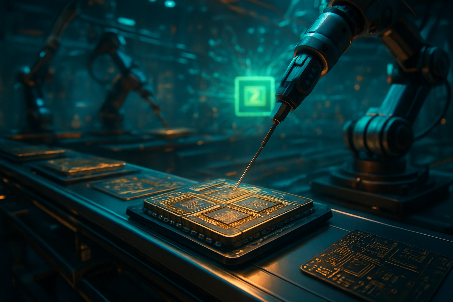
    The Engine of AI: Understanding the CoWoS Breakthrough

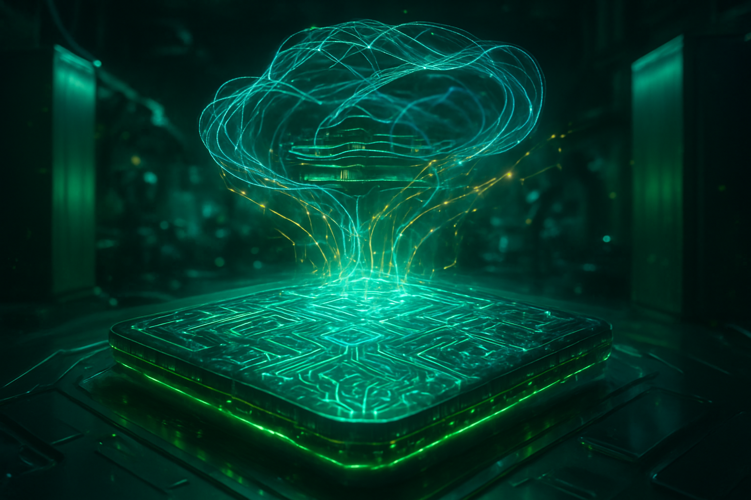
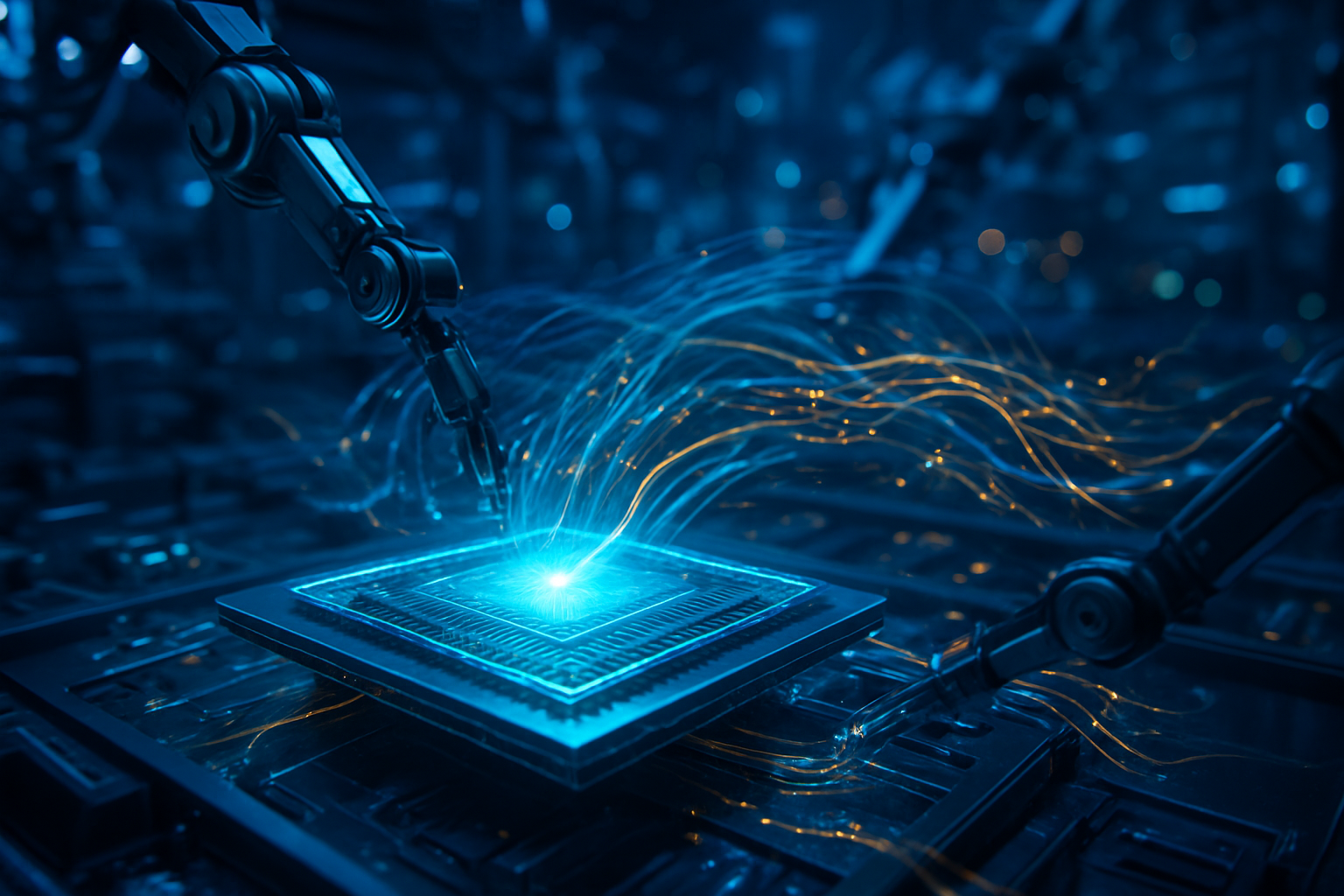
    At the heart of TSMC’s expansion is CoWoS (Chip-on-Wafer-on-Substrate), a 2.5D and 3D packaging technology that allows multiple silicon dies—such as a GPU and several stacks of High Bandwidth Memory (HBM)—to be integrated onto a single interposer. This proximity allows for massive data transfer speeds that are impossible with traditional PCB-based connections. Specifically, TSMC is ramping up production of CoWoS-L (Local Silicon Interconnect), which uses tiny silicon "bridges" to link massive dies that exceed the physical limits of a single lithography exposure, known as the reticle limit.

    This technical shift is essential for the latest generation of AI hardware. For example, the Blackwell architecture from NVIDIA (NASDAQ: NVDA) utilizes two massive GPU dies linked via CoWoS-L to act as a single, unified processor. Early production of these chips faced challenges due to a "Coefficient of Thermal Expansion" (CTE) mismatch, where the different materials in the chip warped at high temperatures. TSMC has since refined the manufacturing process at its Advanced Backend (AP) facilities, particularly at the AP6 site in Zhunan and the newly acquired AP8 facility in Tainan, to improve yields and ensure the structural integrity of these complex multi-die systems.

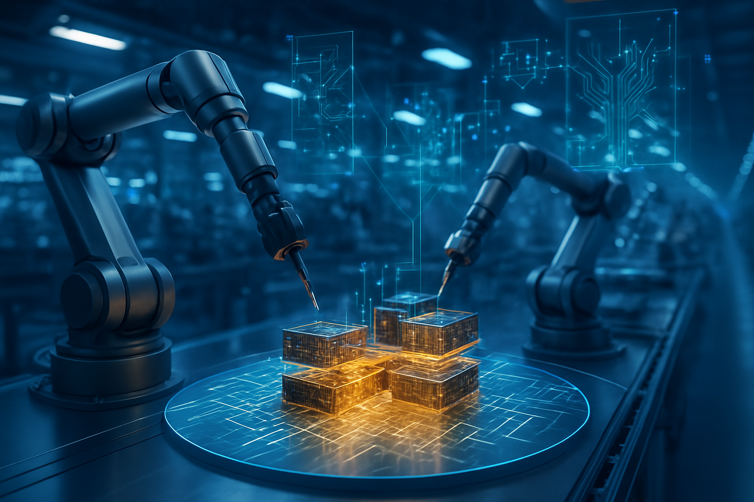
    The 130,000-wafer target will be supported by a sprawling network of new factories. The Chiayi (AP7) complex is poised to become the world’s largest advanced packaging hub, with multiple phases slated to come online between now and 2027. Unlike previous approaches that focused primarily on shrinking transistors (Moore’s Law), TSMC’s strategy for 2026 focuses on "System-on-Integrated-Chips" (SoIC). This approach treats the entire package as a single system, integrating logic, memory, and even power delivery into a three-dimensional stack that offers unprecedented compute density.

    The Competitive Arena: Who Wins in the Capacity Grab?

    The primary beneficiary of this capacity surge is undoubtedly NVIDIA, which is estimated to have secured roughly 60% of TSMC’s total CoWoS allocation for 2026. This guaranteed supply is the backbone of NVIDIA’s roadmap, supporting the full-scale deployment of Blackwell and the early-stage ramp of its successor architecture, Rubin. By securing the lion's share of TSMC's capacity, NVIDIA maintains a strategic "moat" that makes it difficult for competitors to match its volume, even if they have competitive designs.

    However, NVIDIA is not the only player in the queue. Broadcom Inc. (NASDAQ: AVGO) has secured approximately 15% of the capacity to support custom AI ASICs for giants like Google and Meta. Meanwhile, Advanced Micro Devices (NASDAQ: AMD) is using its ~11% allocation to power the Instinct MI350 and MI400 series, which are gaining ground in the enterprise and supercomputing markets. Other major firms, including Marvell Technology, Inc. (NASDAQ: MRVL) and Amazon (NASDAQ: AMZN) through its AWS custom chips, are also vying for space in the 2026 production schedule.

    This expansion also intensifies the rivalry between foundries. While TSMC leads, Intel Corporation (NASDAQ: INTC) is positioning its "Systems Foundry" as a viable alternative, touting its upcoming glass core substrates as a solution to the warping issues seen in organic interposers. Samsung Electronics Co., Ltd. (KRX: 005930) is also pushing its "Turnkey" solution, offering to handle everything from HBM production to advanced packaging under one roof. Nevertheless, TSMC's deep integration with the existing supply chain—including partnerships with Outsourced Semiconductor Assembly and Test (OSAT) leader ASE Technology Holding Co., Ltd. (NYSE: ASX)—gives it a formidable head start.

    The Paradigm Shift: From Silicon Shrinking to System Integration

    TSMC’s massive investment marks a fundamental shift in the broader AI landscape. For decades, the tech industry measured progress by how small a transistor could be made. Today, the "packaging" of those transistors has become just as, if not more, important. This transition suggests that we are entering an era of "More than Moore," where performance gains come from architectural ingenuity and high-density integration rather than just raw process node shrinks.

    The impact of this shift extends to the geopolitical stage. By centralizing the world’s most advanced packaging in Taiwan, TSMC reinforces the island’s strategic importance to the global economy. While efforts are underway to build packaging capacity in the United States—specifically through TSMC's Arizona facilities and Amkor Technology, Inc. (NASDAQ: AMKR)—the vast majority of high-volume, high-yield CoWoS production will remain in Taiwan for the foreseeable future. This concentration of capability creates a "silicon shield" but also remains a point of concern for supply chain resilience experts who fear a single point of failure.

    Furthermore, the environmental and power costs of these ultra-dense chips are becoming a central theme in industry discussions. As TSMC enables chips that consume upwards of 1,000 watts, the focus is shifting toward liquid cooling and more efficient power delivery. The 130,000-wafer-per-month capacity will flood the market with high-performance silicon, but it will be up to data center operators and energy providers to figure out how to power and cool this new wave of AI compute.

    The Road Ahead: Beyond 130,000 Wafers

    Looking toward the late 2020s, the challenges of advanced packaging will only grow. As we move toward HBM4, which features even thinner silicon and higher vertical stacks, the bonding precision required will reach the atomic scale. TSMC is already researching hybrid bonding techniques that eliminate the need for traditional solder bumps entirely, allowing for even tighter integration. The 2026 capacity expansion is just the beginning of a decade-long roadmap toward "wafer-level systems" where a single 300mm wafer could potentially house a whole supercomputer's worth of logic and memory.

    Experts predict that the next major hurdle will be the transition to glass substrates, which offer better thermal stability and flatter surfaces than current organic materials. While TSMC is currently focused on maximizing its CoWoS-L and SoIC technologies, the research and development teams in Hsinchu are undoubtedly watching competitors like Intel closely. The race is no longer just about who can make the smallest transistor, but who can build the most robust and scalable "system-in-package."

    Near-term developments to watch include the specific ramp-up speed of the Chiayi AP7 plant. If TSMC can bring Phase 1 and Phase 2 online ahead of schedule, we may see the AI chip shortage ease by early 2027. However, if equipment lead times for specialized lithography and bonding tools remain high, the 130,000-wafer target might become a moving goalpost, potentially extending the window of high prices and limited availability for AI accelerators.

    A New Era of Compute Density

    TSMC’s decision to double down on CoWoS capacity to 130,000 wafers per month by late 2026 is a watershed moment for the semiconductor industry. It confirms that advanced packaging is the new battlefield of high-performance computing. By nearly quadrupling its output in just two years, TSMC is providing the "fuel" for the generative AI revolution, ensuring that the ambitions of software developers are not limited by the physical constraints of hardware manufacturing.

    In the history of AI, this expansion may be viewed as the moment the industry moved past the "scarcity phase." As supply finally begins to catch up with the astronomical demand from hyperscalers and enterprises, we can expect a shift in focus from merely acquiring hardware to optimizing how that hardware is used. The "Compute Wars" are entering a new phase of high-volume execution.

    For investors and industry watchers, the coming months will be defined by yield rates and construction milestones. Success for TSMC will mean a continued dominance of the foundry market, while any delays could provide an opening for Samsung or Intel to capture disgruntled customers. For now, all eyes are on the construction cranes in Chiayi and Tainan, as they build the foundation for the next generation of artificial intelligence.


    This content is intended for informational purposes only and represents analysis of current AI developments.

    TokenRing AI delivers enterprise-grade solutions for multi-agent AI workflow orchestration, AI-powered development tools, and seamless remote collaboration platforms.
    For more information, visit https://www.tokenring.ai/.

  • The CoWoS Crunch: Why TSMC’s Specialized Packaging Remains the AI Industry’s Ultimate Bottleneck

    The CoWoS Crunch: Why TSMC’s Specialized Packaging Remains the AI Industry’s Ultimate Bottleneck

    As of February 2, 2026, the global artificial intelligence landscape remains in the grip of an "AI super-cycle," where the ability to deploy large-scale models is limited not by software ingenuity, but by the physical architecture of silicon. At the center of this storm is Taiwan Semiconductor Manufacturing Co. (NYSE: TSM), whose advanced packaging technology, Chip-on-Wafer-on-Substrate (CoWoS), has become the single most critical bottleneck in the production of next-generation AI accelerators. Despite a massive capital expenditure push and the rapid commissioning of new facilities, the demand for CoWoS capacity continues to stretch the limits of the semiconductor supply chain.

    The current constraints are driven by the transition to increasingly complex chip architectures, such as NVIDIA’s (NASDAQ: NVDA) Blackwell and the newly debuted Rubin series, which require sophisticated 2.5D and 3D integration to function. While TSMC has successfully scaled its monthly output to record levels, the sheer volume of orders from hyperscalers and chip designers has created a persistent backlog. For the industry's titans, the race for AI dominance is no longer just about who has the best algorithms, but who has secured the most "slots" on TSMC's packaging lines for 2026 and beyond.

    Bridging the Gap: The Technical Evolution of CoWoS-L and CoWoS-S

    At its core, CoWoS is a high-density packaging technology that allows multiple chips—typically a Logic GPU or ASIC alongside several stacks of High Bandwidth Memory (HBM)—to be integrated onto a single substrate. This proximity is vital for AI workloads, which require massive data throughput between the processor and memory. In 2026, the technical challenge has shifted from the traditional CoWoS-S (using a silicon interposer) to the more complex CoWoS-L. This newer variant utilizes Local Silicon Interconnect (LSI) bridges to link multiple active dies, enabling chips that are physically larger than the traditional reticle limit of a single silicon wafer.

    This shift is essential for NVIDIA’s B200 and GB200 Blackwell chips, which effectively act as dual-die processors. The precision required to align these components at the micron level is immense, leading to lower initial yields compared to standard chip manufacturing. Industry experts note that while CoWoS-S was sufficient for the previous H100 generation, the "multi-die" era of 2026 demands the flexibility of CoWoS-L. This complexity is why TSMC’s utilization rates remain at near 100% despite the company’s efforts to automate and expand its Advanced Backend (AP) facilities.

    The Hierarchy of Chips: Who Wins the Capacity War?

    The scramble for packaging capacity has created a clear hierarchy in the semiconductor market. NVIDIA remains the "anchor tenant," reportedly securing roughly 60% of TSMC’s total CoWoS output for the 2026 fiscal year. This dominance has allowed NVIDIA to maintain its lead with the Blackwell series, even as it prepares the 3nm-based Rubin architecture for mass production. However, Advanced Micro Devices (NASDAQ: AMD) has made significant inroads, securing approximately 11% of capacity for its Instinct MI350 and MI400 series, which compete directly for high-end enterprise deployments.

    Beyond the GPU giants, the "Sovereign AI" movement has seen companies like Alphabet Inc. (NASDAQ: GOOGL) and Amazon.com Inc. (NASDAQ: AMZN) bypass standard chip vendors to design their own custom ASICs. Google’s TPU v6 and Amazon’s Trainium 3 chips are now major consumers of CoWoS capacity, often facilitated through design partners like MediaTek (TWSE: 2454). This influx of custom silicon has intensified the competition, forcing smaller AI startups to look toward secondary providers or wait in line for the "spillover" capacity handled by Outsourced Semiconductor Assembly and Test (OSAT) firms like ASE Technology Holding (NYSE: ASX) and Amkor Technology (NASDAQ: AMKR).

    A Global Shift: Beyond the Taiwan Bottleneck

    The CoWoS shortage has sparked a broader conversation about the geographical concentration of advanced packaging. Historically, almost all of TSMC’s advanced packaging was centralized in Taiwan. However, the 2026 landscape shows the first signs of a decentralized model. TSMC’s AP8 facility in Tainan and the newly operational AP7 in Chiayi have been the primary drivers of growth, but the company has recently confirmed plans to establish an advanced packaging hub in Arizona by 2027. This move is seen as a direct response to pressure from the U.S. government to secure a domestic supply chain for critical AI infrastructure.

    Furthermore, the industry is grappling with a secondary bottleneck: High Bandwidth Memory. Even as TSMC expands CoWoS lines, the supply of HBM3e and the emerging HBM4 from vendors like Samsung Electronics (KRX: 005930) is struggling to keep pace. This dual-constraint environment—where both the packaging and the memory are in short supply—has led to a "packaging-bound" era of chip manufacturing. The result is a market where the cost of AI hardware remains high, and the lead times for AI server clusters can still stretch into several months.

    The Road to 2027: Silicon Photonics and HBM4

    Looking ahead, the industry is already preparing for the next technical leap. Predictions for 2027 suggest that CoWoS will evolve to incorporate Silicon Photonics, a technology that uses light instead of electricity to transfer data between chips. This would significantly reduce power consumption—a major concern for data centers currently struggling with the multi-kilowatt demands of Blackwell-based racks. TSMC is reportedly in the early stages of integrating "CPO" (Co-Packaged Optics) into its CoWoS roadmap to address these thermal and power limits.

    Additionally, the transition to HBM4 in late 2026 and 2027 will require even more precise packaging techniques, as the memory stacks move to 12-layer and 16-layer configurations. This will likely keep the pressure on TSMC to continue its aggressive capital investment. Analysts predict that while the extreme supply-demand imbalance may ease slightly by the end of 2026 as Phase 2 of the Chiayi plant reaches full capacity, the long-term trend remains one of hyper-growth, with AI packaging expected to contribute more than 10% of TSMC's total revenue in the coming years.

    Summary: A Redefined Semiconductor Landscape

    The ongoing CoWoS capacity constraints at TSMC have fundamentally redefined what it means to be a chipmaker in the AI era. No longer is it enough to have a brilliant circuit design; companies must now master the intricacies of "System-in-Package" (SiP) logistics and secure a reliable place in the packaging queue. TSMC’s response—building a million-wafer-per-year capacity by the end of 2026—is a testament to the unprecedented scale of the AI revolution.

    As we move through 2026, the industry will be watching for two key indicators: the yield rates of CoWoS-L at the new AP8 facility and the speed at which OSAT partners can absorb the overflow for mid-tier AI applications. For now, the "CoWoS Crunch" remains the defining challenge of the hardware world, a physical limit on the digital aspirations of the world’s most powerful AI models.


    This content is intended for informational purposes only and represents analysis of current AI developments.

    TokenRing AI delivers enterprise-grade solutions for multi-agent AI workflow orchestration, AI-powered development tools, and seamless remote collaboration platforms.
    For more information, visit https://www.tokenring.ai/.

  • NVIDIA Overtakes Apple as TSMC’s Top Customer: The Dawn of the AI Utility Phase

    NVIDIA Overtakes Apple as TSMC’s Top Customer: The Dawn of the AI Utility Phase

    In a watershed moment for the global semiconductor industry, NVIDIA (NASDAQ: NVDA) has officially surpassed Apple (NASDAQ: AAPL) to become the largest revenue contributor for Taiwan Semiconductor Manufacturing Company (TSMC) (NYSE: TSM). Financial data emerging in early 2026 reveals a tectonic shift in the foundry’s client hierarchy: NVIDIA is projected to generate approximately $33 billion in revenue for TSMC this year, accounting for 22% of the total, while Apple, the long-standing "alpha" customer, is expected to contribute $27 billion, or roughly 18%.

    This reversal marks the first time in over a decade that a company other than Apple has held the top spot at the world’s premier chipmaker. The development is more than just a corporate milestone; it signals a fundamental realignment of the global economy. For the past fifteen years, the semiconductor market was largely defined by the smartphone and consumer electronics boom led by Apple. Today, that mantle has passed to the builders of artificial intelligence infrastructure, marking the definitive arrival of the "AI era" in industrial manufacturing.

    The Architecture of Dominance: Blackwell, Rubin, and the CoWoS Bottleneck

    The primary catalyst for this revenue surge is the sheer physical and technical complexity of NVIDIA’s latest silicon architectures. Unlike consumer-grade chips found in iPhones or MacBooks, which are optimized for power efficiency and mass-market costs, NVIDIA’s high-end AI accelerators like the Blackwell Ultra (GB300) and the upcoming Vera Rubin (R100) platforms are massive, high-performance systems. These chips push the boundaries of "reticle size"—the maximum area a single chip can occupy on a wafer—often requiring multiple dies to be stitched together with extreme precision. This complexity allows TSMC to command significantly higher prices per wafer compared to the smaller, more streamlined A-series chips produced for Apple.

    A critical component of this revenue growth is TSMC’s Chip on Wafer on Substrate (CoWoS) packaging technology. As AI models demand faster data throughput, the "glue" that connects GPUs with High-Bandwidth Memory (HBM) has become the industry’s most valuable bottleneck. NVIDIA has reportedly secured nearly 60% of TSMC’s entire CoWoS capacity for 2026. This advanced packaging is a high-margin service that adds a substantial layer of revenue on top of traditional wafer fabrication. By late 2026, TSMC’s CoWoS capacity is expected to reach over 100,000 wafers per month to keep pace with NVIDIA’s relentless release cycle.

    Initial reactions from the semiconductor research community suggest that NVIDIA’s move to the top spot was inevitable given the massive die sizes of the Rubin architecture. Analysts note that while Apple still ships hundreds of millions more individual chips than NVIDIA, the "value-per-wafer" for an AI accelerator is orders of magnitude higher. Industry experts believe this creates a "priority lock" where NVIDIA now gets first access to TSMC's most advanced nodes, such as the upcoming 2nm (N2) process, a privilege previously reserved almost exclusively for Apple.

    Reshaping the Tech Titan Hierarchy

    This shift has profound implications for the competitive landscape of Big Tech. For years, Apple’s dominance at TSMC gave it a strategic "moat," ensuring its products had the most efficient processors on the market before anyone else. Now, with NVIDIA as the primary revenue driver, TSMC is increasingly incentivized to prioritize the high-performance computing (HPC) requirements of AI over the low-power requirements of mobile devices. This could potentially slow the pace of performance gains in consumer hardware while accelerating the capabilities of the data centers that power AI services.

    Major AI labs and cloud providers—including Microsoft (NASDAQ: MSFT), Amazon (NASDAQ: AMZN), and Alphabet (NASDAQ: GOOGL)—stand to benefit from this alignment, as NVIDIA’s primary status ensures a steady, albeit expensive, supply of the hardware needed to scale their generative AI products. However, the high cost of NVIDIA’s Rubin platform, which targets a 10x reduction in token generation costs, creates a high barrier to entry for smaller startups. These companies must now navigate a market where the "silicon tax" is increasingly paid to a single, dominant provider that sits at the top of the manufacturing food chain.

    The strategic advantage has clearly pivoted. NVIDIA's ability to command TSMC’s roadmap means the foundry is now optimizing its future factories for "big silicon" rather than "small silicon." This transition forces competitors like AMD (NASDAQ: AMD) to compete for the remaining advanced packaging capacity, potentially tightening the supply of rival AI chips and further cementing NVIDIA’s market positioning as the de facto gatekeeper of AI compute.

    Entering the 'Utility Phase' of the AI Cycle

    Market analysts are describing this period as the transition from the "Land Grab Phase" to the "Utility Phase" of the AI cycle. During 2023 and 2024, the industry saw a frantic, speculative rush to acquire any available GPUs to avoid being left behind. In 2026, the focus has shifted toward Return on Investment (ROI) and enterprise-wide productivity. AI is no longer a peripheral experiment; it has become a core utility, as essential to modern business as electricity or high-speed internet.

    The fact that NVIDIA has overtaken Apple—a company built on consumer desire—indicates that the AI cycle is now driven by industrial necessity. This stage of the cycle requires a drastic reduction in the cost of intelligence to remain sustainable. This is why the Rubin architecture is so significant; by focusing on slashing the cost per token, NVIDIA is making it economically viable for businesses to embed AI into every layer of their software stacks. It represents a move toward the commoditization of high-level reasoning.

    Comparatively, this milestone is being likened to the moment in the early 20th century when industrial power generation surpassed residential lighting as the primary driver of the electrical grid. The sheer scale of infrastructure being built suggests that we are move past the "hype" and into a decade-long deployment phase. While concerns about an "AI bubble" persist, the hard capital expenditures flowing from the world’s most valuable companies into TSMC’s foundries suggest a long-term commitment to this technological pivot.

    The Horizon: 2nm and Beyond

    Looking ahead, the next battleground will be the transition to the 2nm (N2) process node, expected to ramp up in late 2026 and 2027. Experts predict that NVIDIA will be the lead customer for this node, utilizing "GAAFET" (Gate-All-Around Field-Effect Transistor) technology to further increase the density of its Rubin-successor chips. The challenge will not just be fabrication, but the continued scaling of HBM and advanced packaging, which remain prone to yield issues and supply chain disruptions.

    In the near term, we can expect NVIDIA to push deeper into vertical integration, perhaps offering more tailored "AI factories" that include not just the chips, but the liquid cooling and networking stacks required to run them. The goal is to move from selling components to selling entire units of "intelligence." Challenges remain, particularly regarding the massive power consumption of these new data centers and the geopolitical tensions surrounding semiconductor manufacturing in the Taiwan Strait, which remains a singular point of failure for the global AI economy.

    A New Era in Computing History

    The ascension of NVIDIA to the top of TSMC’s customer list is a historic realignment that marks the end of the mobile-first era and the beginning of the AI-first era. It underscores a shift in value from the device in our pockets to the massive, distributed intelligence engines in the cloud. NVIDIA’s $33 billion contribution to TSMC’s coffers is the ultimate proof of the industry's belief in the permanence of the AI revolution.

    As we move through 2026, the key metrics to watch will be the "cost-per-token" metrics provided by the Rubin platform and the speed at which TSMC can expand its CoWoS capacity. If NVIDIA can continue to lower the cost of AI while maintaining its lead at the foundry, it will solidify its role as the foundational utility of the 21st century. The world is no longer just buying gadgets; it is building a new kind of cognitive infrastructure, and for the first time, the numbers at the world's most important factory prove it.


    This content is intended for informational purposes only and represents analysis of current AI developments.

    TokenRing AI delivers enterprise-grade solutions for multi-agent AI workflow orchestration, AI-powered development tools, and seamless remote collaboration platforms.
    For more information, visit https://www.tokenring.ai/.

  • The CoWoS Conundrum: Why Advanced Packaging is the ‘Sovereign Utility’ of the 2026 AI Economy

    The CoWoS Conundrum: Why Advanced Packaging is the ‘Sovereign Utility’ of the 2026 AI Economy

    As of January 28, 2026, the global race for artificial intelligence dominance is no longer being fought solely in the realm of algorithmic breakthroughs or raw transistor counts. Instead, the front line of the AI revolution has moved to a high-precision manufacturing stage known as "Advanced Packaging." At the heart of this struggle is Taiwan Semiconductor Manufacturing Company (TSMC) (NYSE: TSM), whose proprietary CoWoS (Chip on Wafer on Substrate) technology has become the single most critical bottleneck in the production of high-end AI accelerators. Despite a multi-billion dollar expansion blitz, the supply of CoWoS capacity remains "structurally oversubscribed," dictating the pace at which the world’s tech giants can deploy their next-generation models.

    The immediate significance of this bottleneck cannot be overstated. In early 2026, the ability to secure CoWoS allocation is directly correlated with a company’s market valuation and its competitive standing in the AI landscape. While the industry has seen massive leaps in GPU architecture, those chips are useless without the high-bandwidth memory (HBM) integration that CoWoS provides. This technical "chokepoint" has effectively divided the tech world into two camps: those who have secured TSMC’s 2026 capacity—most notably NVIDIA (NASDAQ: NVDA)—and those currently scrambling for "second-source" alternatives or waiting in an 18-month-long production queue.

    The Engineering of a Bottleneck: Inside the CoWoS Architecture

    Technically, CoWoS is a 2.5D packaging technology that allows for the integration of multiple silicon dies—typically a high-performance logic GPU and several stacks of High-Bandwidth Memory (HBM4 in 2026)—onto a single, high-density interposer. Unlike traditional packaging, which connects a finished chip to a circuit board using relatively coarse wires, CoWoS creates microscopic interconnections that enable massive data throughput between the processor and its memory. This "memory wall" is the primary obstacle in training Large Language Models (LLMs); without the ultra-fast lanes provided by CoWoS, the world’s most powerful GPUs would spend the majority of their time idling, waiting for data.

    In 2026, the technology has evolved into three distinct flavors to meet varying industry needs. CoWoS-S (Silicon) remains the legacy standard, using a monolithic silicon interposer that is now facing physical size limits. To break this "reticle limit," TSMC has pivoted aggressively toward CoWoS-L (Local Silicon Interconnect), which uses small silicon "bridges" embedded in an organic layer. This allows for massive packages up to 6 times the size of a standard chip, supporting up to 16 HBM4 stacks. Meanwhile, CoWoS-R (Redistribution Layer) offers a cost-effective organic alternative for high-speed networking chips from companies like Broadcom (NASDAQ: AVGO) and Cisco (NASDAQ: CSCO).

    The reason scaling this technology is so difficult lies in its environmental and precision requirements. Advanced packaging now requires cleanroom standards that rival front-end wafer fabrication—specifically ISO Class 5 environments where fewer than 3,500 microscopic particles exist per cubic meter. Furthermore, the specialized tools required for this process, such as hybrid bonders from Besi and high-precision lithography tools from ASML (NASDAQ: ASML), currently have lead times exceeding 12 to 18 months. Even with TSMC’s massive $56 billion capital expenditure budget for 2026, the physical reality of building these ultra-clean facilities and waiting for precision equipment means that the supply-demand gap will not fully close until at least 2027.

    A Two-Tiered AI Industry: Winners and Losers in the Capacity War

    The scarcity of CoWoS capacity has created a stark divide in the corporate hierarchy. NVIDIA (NASDAQ: NVDA) remains the undisputed king of the hill, having used its massive cash reserves to pre-book approximately 60% of TSMC’s total 2026 CoWoS output. This strategic move has ensured that its Rubin and Blackwell Ultra architectures remain the dominant hardware for hyperscalers like Microsoft and Meta. For NVIDIA, CoWoS isn't just a technical spec; it is a defensive moat that prevents competitors from scaling their hardware even if they have superior designs on paper.

    In contrast, other major players are forced to navigate a more precarious path. AMD (NASDAQ: AMD), while holding a respectable 11% allocation for its MI355 and MI400 series, has begun qualifying "second-source" packaging partners like ASE Group and Amkor to mitigate its reliance on TSMC. This diversification strategy is risky, as shifting packaging providers can impact yields and performance, but it is a necessary gamble in an environment where TSMC's "wafer starts per month" are spoken for years in advance. Meanwhile, custom silicon efforts from Google and Amazon (via Broadcom) occupy another 15% of the market, leaving startups and second-tier AI labs to fight over the remaining 14% of capacity, often at significantly higher "spot market" prices.

    This dynamic has also opened a door for Intel (NASDAQ: INTC). Recognizing the bottleneck, Intel has positioned its "Foundry" business as a turnkey packaging alternative. In early 2026, Intel is pitching its EMIB (Embedded Multi-die Interconnect Bridge) and Foveros 3D packaging technologies to customers who may have their chips fabricated at TSMC but want to avoid the CoWoS waitlist. This "open foundry" model is Intel’s best chance at reclaiming market share, as it offers a faster time-to-market for companies that are currently "capacity-starved" by the TSMC logjam.

    Geopolitics and the Shift from Moore’s Law to 'More than Moore'

    The CoWoS bottleneck represents a fundamental shift in the semiconductor industry's philosophy. For decades, "Moore’s Law"—the doubling of transistors on a single chip—was the primary driver of progress. However, as we approach the physical limits of silicon atoms, the industry has shifted toward "More than Moore," an era where performance gains come from how chips are integrated and packaged together. In this new paradigm, the "packaging house" is just as strategically important as the "fab." This has elevated TSMC from a manufacturing partner to what analysts are calling a "Sovereign Utility of Computation."

    This concentration of power in Taiwan has significant geopolitical implications. In early 2026, the "Silicon Shield" is no longer just about the chips themselves, but about the unique CoWoS lines in facilities like the new Chiayi AP7 plant. Governments around the world are now waking up to the fact that "Sovereign AI" requires not just domestic data centers, but a domestic advanced packaging supply chain. This has spurred massive subsidies in the U.S. and Europe to bring packaging capacity closer to home, though these projects are still years away from reaching the scale of TSMC’s Taiwanese operations.

    The environmental and resource concerns of this expansion are also coming to the forefront. The high-precision bonding and thermal management required for CoWoS-L packages consume significant amounts of energy and ultrapure water. As TSMC scales to its target of 150,000 wafer starts per month by the end of 2026, the strain on Taiwan’s infrastructure has become a central point of debate, highlighting the fragile foundation upon which the global AI boom is built.

    Beyond the Silicon Interposer: The Future of Integration

    Looking past the current 2026 bottleneck, the industry is already preparing for the next evolution in integration: glass substrates. Intel has taken an early lead in this space, launching its first chips using glass cores in early 2026. Glass offers superior flatness and thermal stability compared to the organic materials currently used in CoWoS, potentially solving the "warpage" issues that plague the massive 6x reticle-sized chips of the future.

    We are also seeing the rise of "System on Integrated Chips" (SoIC), a true 3D stacking technology that eliminates the interposer entirely by bonding chips directly on top of one another. While currently more expensive and difficult to manufacture than CoWoS, SoIC is expected to become the standard for the "Super-AI" chips of 2027 and 2028. Experts predict that the transition from 2.5D (CoWoS) to 3D (SoIC) will be the next major battleground, with Samsung (OTC: SSNLF) betting heavily on its "Triple Alliance" of memory, foundry, and packaging to leapfrog TSMC in the 3D era.

    The challenge for the next 24 months will be yield management. As packages become larger and more complex, a single defect in one of the eight HBM stacks or the central GPU can ruin the entire multi-thousand-dollar assembly. The development of "repairable" or "modular" packaging techniques is a major area of research for 2026, as manufacturers look for ways to salvage these high-value components when a single connection fails during the bonding process.

    Final Assessment: The Road Through 2026

    The CoWoS bottleneck is the defining constraint of the 2026 AI economy. While TSMC’s aggressive capacity expansion is slowly beginning to bear fruit, the "insatiable" demand from NVIDIA and the hyperscalers ensures that advanced packaging will remain a seller’s market for the foreseeable future. We have entered an era where "computing power" is a physical commodity, and its availability is determined by the precision of a few dozen high-tech bonding machines in northern Taiwan.

    As we move into the second half of 2026, watch for the ramp-up of Samsung’s Taylor, Texas facility and Intel’s ability to win over "CoWoS refugees." The successful mass production of glass substrates and the maturation of 3D SoIC technology will be the key indicators of who wins the next phase of the AI war. For now, the world remains tethered to TSMC's packaging lines—a microscopic bridge that supports the weight of the entire global AI industry.


    This content is intended for informational purposes only and represents analysis of current AI developments.

    TokenRing AI delivers enterprise-grade solutions for multi-agent AI workflow orchestration, AI-powered development tools, and seamless remote collaboration platforms.
    For more information, visit https://www.tokenring.ai/.

  • The CoWoS Stranglehold: TSMC Ramps Advanced Packaging as AI Demand Outpaces the Physics of Supply

    The CoWoS Stranglehold: TSMC Ramps Advanced Packaging as AI Demand Outpaces the Physics of Supply

    As of late January 2026, the artificial intelligence industry finds itself in a familiar yet intensified paradox: despite a historic, multi-billion-dollar expansion of semiconductor manufacturing capacity, the "Compute Crunch" remains the defining characteristic of the tech landscape. At the heart of this struggle is Taiwan Semiconductor Manufacturing Co. (TPE: 2330) and its Chip-on-Wafer-on-Substrate (CoWoS) advanced packaging technology. While TSMC has successfully quadrupled its CoWoS output compared to late 2024 levels, the insatiable hunger of generative AI models has kept the supply chain in a state of perpetual "catch-up," making advanced packaging the ultimate gatekeeper of global AI progress.

    This persistent bottleneck is the physical manifestation of Item 9 on our Top 25 AI Developments list: The Infrastructure Ceiling. As AI models shift from the trillion-parameter Blackwell era into the multi-trillion-parameter Rubin era, the limiting factor is no longer just how many transistors can be etched onto a wafer, but how many high-bandwidth memory (HBM) modules and logic dies can be fused together into a single, high-performance package.

    The Technical Frontier: Beyond Simple Silicon

    The current state of CoWoS in early 2026 is a far cry from the nascent stages of two years ago. TSMC’s AP6 facility in Zhunan is now operating at peak capacity, serving as the workhorse for NVIDIA's (NASDAQ: NVDA) Blackwell series. However, the technical specifications have evolved. We are now seeing the widespread adoption of CoWoS-L, which utilizes local silicon interconnects (LSI) to bridge chips, allowing for larger package sizes that exceed the traditional "reticle limit" of a single chip.

    Technical experts point out that the integration of HBM4—the latest generation of High Bandwidth Memory—has added a new layer of complexity. Unlike previous iterations, HBM4 requires a more intricate 2048-bit interface, necessitating the precision that only TSMC’s advanced packaging can provide. This transition has rendered older "on-substrate" methods obsolete for top-tier AI training, forcing the entire industry to compete for the same limited CoWoS-L and SoIC (System on Integrated Chips) lines. The industry reaction has been one of cautious awe; while the throughput of these packages is unprecedented, the yields for such complex "chiplets" remain a closely guarded secret, frequently cited as the reason for the continued delivery delays of enterprise-grade AI servers.

    The Competitive Arena: Winners, Losers, and the Arizona Pivot

    The scarcity of CoWoS capacity has created a rigid hierarchy in the tech sector. NVIDIA remains the undisputed king of the queue, reportedly securing nearly 60% of TSMC’s total 2026 capacity to fuel its transition to the Rubin (R100) architecture. This has left rivals like AMD (NASDAQ: AMD) and custom silicon giants like Broadcom (NASDAQ: AVGO) and Marvell Technology (NASDAQ: MRVL) in a fierce battle for the remaining slots. For hyperscalers like Google and Amazon, who are increasingly designing their own AI accelerators (TPUs and Trainium), the CoWoS bottleneck represents a strategic risk that has forced them to diversify their packaging partners.

    To mitigate this, a landmark collaboration has emerged between TSMC and Amkor Technology (NASDAQ: AMKR). In a strategic move to satisfy U.S. "chips-act" requirements and provide geographical redundancy, the two firms have established a turnkey advanced packaging line in Peoria, Arizona. This allows TSMC to perform the front-end "Chip-on-Wafer" process in its Phoenix fabs while Amkor handles the "on-Substrate" finishing nearby. While this has provided a pressure valve for North American customers, it has not yet solved the global shortage, as the most advanced "Phase 1" of TSMC’s massive AP7 plant in Chiayi, Taiwan, has faced minor delays, only just beginning its equipment move-in this quarter.

    A Wider Significance: Packaging is the New Moore’s Law

    The CoWoS saga underscores a fundamental shift in the semiconductor industry. For decades, progress was measured by the shrinking size of transistors. Today, that progress has shifted to "More than Moore" scaling—using advanced packaging to stack and stitch together multiple chips. This is why advanced packaging is now a primary revenue driver, expected to contribute over 10% of TSMC’s total revenue by the end of 2026.

    However, this shift brings significant geopolitical and environmental concerns. The concentration of advanced packaging in Taiwan remains a point of vulnerability for the global AI economy. Furthermore, the immense power requirements of these multi-die packages—some consuming over 1,000 watts per unit—have pushed data center cooling technologies to their limits. Comparisons are often drawn to the early days of the jet engine: we have the power to reach incredible speeds, but the "materials science" of the engine (the package) is now the primary constraint on how fast we can go.

    The Road Ahead: Panel-Level Packaging and Beyond

    Looking toward the horizon of 2027 and 2028, TSMC is already preparing for the successor to CoWoS: CoPoS (Chip-on-Panel-on-Substrate). By moving from circular silicon wafers to large rectangular glass panels, TSMC aims to increase the area of the packaging surface by several multiples, allowing for even larger "AI Super-Chips." Experts predict this will be necessary to support the "Rubin Ultra" chips expected in late 2027, which are rumored to feature even more HBM stacks than the current Blackwell-Ultra configurations.

    The challenge remains the "yield-to-complexity" ratio. As packages become larger and more complex, the chance of a single defect ruining a multi-thousand-dollar assembly increases. The industry is watching closely to see if TSMC’s Arizona AP1 facility, slated for construction in the second half of this year, can replicate the high yields of its Taiwanese counterparts—a feat that has historically proven difficult.

    Wrapping Up: The Infrastructure Ceiling

    In summary, TSMC’s Herculean efforts to ramp CoWoS capacity to 120,000+ wafers per month by early 2026 are a testament to the company's engineering prowess, yet they remain insufficient against the backdrop of the global AI gold rush. The bottleneck has shifted from "can we make the chip?" to "can we package the system?" This reality cements Item 9—The Infrastructure Ceiling—as the most critical challenge for AI developers today.

    As we move through 2026, the key indicators to watch will be the operational ramp of the Chiayi AP7 plant and the success of the Amkor-TSMC Arizona partnership. For now, the AI industry remains strapped to the pace of TSMC’s cleanrooms. The long-term impact is clear: those who control the packaging, control the future of artificial intelligence.


    This content is intended for informational purposes only and represents analysis of current AI developments.

    TokenRing AI delivers enterprise-grade solutions for multi-agent AI workflow orchestration, AI-powered development tools, and seamless remote collaboration platforms.
    For more information, visit https://www.tokenring.ai/.

  • The Rubin Era: NVIDIA’s Strategic Stranglehold on Advanced Packaging Redefines the AI Arms Race

    The Rubin Era: NVIDIA’s Strategic Stranglehold on Advanced Packaging Redefines the AI Arms Race

    As the tech industry pivots into 2026, NVIDIA (NASDAQ: NVDA) has fundamentally shifted the theater of war in the artificial intelligence sector. No longer is the battle fought solely on transistor counts or software moats; the new frontier is "advanced packaging." By securing approximately 60% of Taiwan Semiconductor Manufacturing Company's (NYSE: TSM) total Chip-on-Wafer-on-Substrate (CoWoS) capacity for the fiscal year—estimated at a staggering 700,000 to 850,000 wafers—NVIDIA has effectively cornered the market on the high-performance hardware necessary to power the next generation of autonomous AI agents.

    The announcement of the 'Rubin' platform (R100) at CES 2026 marks the official transition from the Blackwell architecture to a system-on-rack paradigm designed specifically for "Agentic AI." With this strategic lock on TSMC’s production lines, industry analysts have dubbed advanced packaging the "new currency" of the tech sector. While competitors scramble for the remaining 40% of the world's high-end assembly capacity, NVIDIA has built a logistical moat that may prove even more formidable than its CUDA software dominance.

    The Technical Leap: R100, HBM4, and the Vera Architecture

    The Rubin R100 is more than an incremental upgrade; it is a specialized engine for the era of reasoning. Manufactured on TSMC’s enhanced 3nm (N3P) process, the Rubin GPU packs a massive 336 billion transistors—a 1.6x density improvement over the Blackwell series. However, the most critical technical shift lies in the memory. Rubin is the first platform to fully integrate HBM4 (High Bandwidth Memory 4), featuring eight stacks that provide 288GB of capacity and a blistering 22 TB/s of bandwidth. This leap is made possible by a 2048-bit interface, doubling the width of HBM3e and finally addressing the "memory wall" that has plagued large language model (LLM) scaling.

    The platform also introduces the Vera CPU, which replaces the Grace series with 88 custom "Olympus" ARM cores. This CPU is architected to handle the complex orchestration required for multi-step AI reasoning rather than just simple data processing. To tie these components together, NVIDIA has transitioned entirely to CoWoS-L (Local Silicon Interconnect) packaging. This technology uses microscopic silicon bridges to "stitch" together multiple compute dies and memory stacks, allowing for a package size that is four to six times the limit of a standard lithographic reticle. Initial reactions from the research community highlight that Rubin’s 100-petaflop FP4 performance effectively halves the cost of token inference, bringing the dream of "penny-per-million-tokens" into reality.

    A Supply Chain Stranglehold: Packaging as the Strategic Moat

    NVIDIA’s decision to book 60% of TSMC’s CoWoS capacity for 2026 has sent shockwaves through the competitive landscape. Advanced Micro Devices (NASDAQ: AMD) and Intel Corporation (NASDAQ: INTC) now find themselves in a high-stakes game of musical chairs. While AMD’s new Instinct MI400 offers a competitive 432GB of HBM4, its ability to scale to the demands of hyperscalers is now physically limited by the available slots at TSMC’s AP8 and AP7 fabs. Analysts at Wedbush have noted that in 2026, "having the best chip design is useless if you don't have the CoWoS allocation to build it."

    In response to this bottleneck, major hyperscalers like Meta Platforms (NASDAQ: META) and Amazon (NASDAQ: AMZN) have begun diversifying their custom ASIC strategies. Meta has reportedly diverted a portion of its MTIA (Meta Training and Inference Accelerator) production to Intel’s packaging facilities in Arizona, utilizing Intel’s EMIB (Embedded Multi-Die Interconnect Bridge) technology as a hedge against the TSMC shortage. Despite these efforts, NVIDIA’s pre-emptive strike on the supply chain ensures that it remains the "default choice" for any organization looking to deploy AI at scale in the coming 24 months.

    Beyond Generative AI: The Rise of Agentic Infrastructure

    The broader significance of the Rubin platform lies in its optimization for "Agentic AI"—systems capable of autonomous planning and execution. Unlike the generative models of 2024 and 2025, which primarily predicted the next word in a sequence, 2026’s models are focused on "multi-turn reasoning." This shift requires hardware with ultra-low latency and persistent memory storage. NVIDIA has met this need by integrating Co-Packaged Optics (CPO) directly into the Rubin package, replacing copper transceivers with fiber optics to reduce inter-GPU communication power by 5x.

    This development signals a maturation of the AI landscape from a "gold rush" of model training to a "utility phase" of execution. The Rubin NVL72 rack-scale system, which integrates 72 Rubin GPUs, acts as a single massive computer with 260 TB/s of aggregate bandwidth. This infrastructure is designed to support thousands of autonomous agents working in parallel on tasks ranging from drug discovery to automated software engineering. The concern among some industry watchdogs, however, is the centralization of this power. With NVIDIA controlling the packaging capacity, the pace of AI innovation is increasingly dictated by a single company’s roadmap.

    The Future Roadmap: Glass Substrates and Panel-Level Scaling

    Looking beyond the 2026 rollout of Rubin, NVIDIA and TSMC are already preparing for the next physical frontier: Fan-Out Panel-Level Packaging (FOPLP). Current CoWoS technology is limited by the circular 300mm silicon wafers on which chips are built, leading to significant wasted space at the edges. By 2027 and 2028, NVIDIA is expected to transition to large rectangular glass or organic panels (600mm x 600mm) for its "Feynman" architecture.

    This transition will allow for three times as many chips per carrier, potentially easing the capacity constraints that defined the 2025-2026 era. Experts predict that glass substrates will become the standard by 2028, offering superior thermal stability and even higher interconnect density. However, the immediate challenge remains the yield rates of these massive panels. For now, the industry’s eyes are on the Rubin ramp-up in the second half of 2026, which will serve as the ultimate test of whether NVIDIA’s "packaging first" strategy can sustain its 1000% growth trajectory.

    A New Chapter in Computing History

    The launch of the Rubin platform and the strategic capture of TSMC’s CoWoS capacity represent a pivotal moment in semiconductor history. NVIDIA has successfully transformed itself from a chip designer into a vertically integrated infrastructure provider that controls the most critical bottlenecks in the global economy. By securing 60% of the world's most advanced assembly capacity, the company has effectively decided the winners and losers of the 2026 AI cycle before the first Rubin chip has even shipped.

    In the coming months, the industry will be watching for the first production yields of the R100 and the success of HBM4 integration from suppliers like SK Hynix (KRX: 000660), Samsung Electronics (KRX: 005930), and Micron Technology (NASDAQ: MU). As packaging continues to be the "new currency," the ability to innovate within these physical constraints will define the next decade of artificial intelligence. For now, the "Rubin Era" has begun, and the world’s compute capacity is firmly in NVIDIA’s hands.


    This content is intended for informational purposes only and represents analysis of current AI developments.

    TokenRing AI delivers enterprise-grade solutions for multi-agent AI workflow orchestration, AI-powered development tools, and seamless remote collaboration platforms.
    For more information, visit https://www.tokenring.ai/.

  • The Great Unclogging: TSMC Commits $56 Billion Capex to Double CoWoS Capacity for NVIDIA’s Rubin Era

    The Great Unclogging: TSMC Commits $56 Billion Capex to Double CoWoS Capacity for NVIDIA’s Rubin Era

    TAIPEI, Taiwan — In a definitive move to cement its dominance over the global AI supply chain, Taiwan Semiconductor Manufacturing Company (NYSE: TSM) has officially entered a "capex supercycle," announcing a staggering $52 billion to $56 billion capital expenditure budget for 2026. The announcement, delivered during the company's January 15 earnings call, signals the end of the "Great AI Hardware Bottleneck" that has plagued the industry for the better part of three years. By scaling its proprietary CoWoS (Chip-on-Wafer-on-Substrate) advanced packaging capacity to a projected 130,000—and potentially 150,000—wafers per month by late 2026, TSMC is effectively industrializing the production of next-generation AI accelerators.

    This massive expansion is largely a response to "insane" demand from NVIDIA (NASDAQ: NVDA), which has reportedly secured over 60% of TSMC’s 2026 packaging capacity to support the launch of its Rubin architecture. As AI models grow in complexity, the industry is shifting away from monolithic chips toward "chiplets," making advanced packaging—once a niche back-end process—the most critical frontier in semiconductor manufacturing. TSMC’s strategic pivot treats packaging not as an afterthought, but as a primary revenue driver that is now fundamentally inseparable from the fabrication of the world’s most advanced 2nm and A16 nodes.

    Breaking the Reticle Limit: The Rise of CoWoS-L

    The technical centerpiece of this expansion is CoWoS-L (Local Silicon Interconnect), a sophisticated packaging technology designed to bypass the physical limitations of traditional silicon manufacturing. In standard chipmaking, the "reticle limit" defines the maximum size of a single chip (roughly 858mm²). However, NVIDIA’s upcoming Rubin (R100) GPUs and the current Blackwell Ultra (B300) series require a surface area far larger than any single piece of silicon can provide. CoWoS-L solves this by using small silicon "bridges" embedded in an organic layer to interconnect multiple compute dies and High Bandwidth Memory (HBM) stacks.

    Unlike the older CoWoS-S, which used a solid silicon interposer and was limited in size and yield, CoWoS-L allows for massive "Superchips" that can be up to six times the standard reticle size. This enables NVIDIA to "stitch" together its GPU dies with 12 or even 16 stacks of next-generation HBM4 memory, providing the terabytes of bandwidth required for trillion-parameter AI models. Industry experts note that the transition to CoWoS-L is technically demanding; during a recent media tour of TSMC’s new Chiayi AP7 facility on January 22, engineers highlighted that the alignment precision required for these silicon bridges is measured in nanometers, representing a quantum leap over the packaging standards of just two years ago.

    The "Compute Moat": Consolidating the AI Hierarchy

    TSMC’s capacity expansion creates a strategic "compute moat" for its largest customers, most notably NVIDIA. By pre-booking the lion's share of the 130,000 monthly wafers, NVIDIA has effectively throttled the ability of competitors like AMD (NASDAQ: AMD) and Intel (NASDAQ: INTC) to scale their own high-end AI offerings. While AMD’s Instinct MI400 series is expected to utilize similar packaging techniques, the sheer volume of TSMC’s commitment to NVIDIA suggests that "Team Green" will maintain its lead in time-to-market for the Rubin R100, which is slated for full production in late 2026.

    This expansion also benefits "hyperscale" custom silicon designers. Companies like Broadcom (NASDAQ: AVGO) and Marvell (NASDAQ: MRVL), which design bespoke AI chips for Google (NASDAQ: GOOGL) and Amazon (NASDAQ: AMZN), are also vying for a slice of the CoWoS-L pie. However, the $56 billion capex plan underscores a shift in power: TSMC is no longer just a "dumb pipe" for wafer fabrication; it is the gatekeeper of AI performance. Startups and smaller chip designers may find themselves pushed toward Outsourced Semiconductor Assembly and Test (OSAT) partners like Amkor Technology (NASDAQ: AMKR), as TSMC prioritizes high-margin, high-complexity orders from the "Big Three" of AI.

    The Geopolitics of the Chiplet Era

    The broader significance of TSMC’s 2026 roadmap lies in the realization that the "Chiplet Era" is officially here. We are witnessing a fundamental change in the semiconductor landscape where performance gains are coming from how chips are assembled, rather than just how small their transistors are. This shift has profound implications for global supply chain stability. By concentrating its advanced packaging facilities in sites like Chiayi and Taichung, TSMC is centralizing the world’s AI "brain" production. While this provides unprecedented efficiency, it also heightens the stakes for geopolitical stability in the Taiwan Strait.

    Furthermore, the easing of the CoWoS bottleneck marks a transition from a "supply-constrained" AI market to a "demand-validated" one. For the past two years, AI growth was limited by how many GPUs could be built; by 2026, the limit will be how much power data centers can draw and how efficiently developers can utilize the massive compute pools being deployed. The transition to HBM4, which requires the complex interfaces provided by CoWoS-L, will be the true test of this new infrastructure, potentially leading to a 3x increase in memory bandwidth for LLM (Large Language Model) training compared to 2024 levels.

    The Horizon: Panel-Level Packaging and Beyond

    Looking beyond the 130,000 wafer-per-month milestone, the industry is already eyeing the next frontier: Panel-Level Packaging (PLP). TSMC has begun pilot-testing rectangular "Panel" substrates, which offer three to four times the usable surface area of a traditional 300mm circular wafer. If successful, this could further reduce costs and increase the output of AI chips in 2027 and 2028. Additionally, the integration of "Glass Substrates" is on the long-term roadmap, promising even higher thermal stability and interconnect density for the post-Rubin era.

    Challenges remain, particularly in power delivery and heat dissipation. As CoWoS-L allows for larger and hotter chip clusters, TSMC and its partners are heavily investing in liquid cooling and "on-chip" power management solutions. Analysts predict that by late 2026, the focus of the AI hardware race will shift from "packaging capacity" to "thermal management efficiency," as the industry struggles to keep these multi-thousand-watt monsters from melting.

    Summary and Outlook

    TSMC’s $56 billion capex and its 130,000-wafer CoWoS target represent a watershed moment for the AI industry. It is a massive bet on the longevity of the AI boom and a vote of confidence in NVIDIA’s Rubin roadmap. The move effectively ends the era of hardware scarcity, potentially lowering the barrier to entry for large-scale AI deployment while simultaneously concentrating power in the hands of the few companies that can afford TSMC’s premium services.

    As we move through 2026, the key metrics to watch will be the yield rates of the new Chiayi AP7 facility and the first real-world performance benchmarks of HBM4-equipped Rubin GPUs. For now, the message from Taipei is clear: the bottleneck is breaking, and the next phase of the AI revolution will be manufactured at a scale never before seen in human history.


    This content is intended for informational purposes only and represents analysis of current AI developments.

    TokenRing AI delivers enterprise-grade solutions for multi-agent AI workflow orchestration, AI-powered development tools, and seamless remote collaboration platforms.
    For more information, visit https://www.tokenring.ai/.

  • The Great Packaging Surge: TSMC Targets 150,000 CoWoS Wafers to Fuel NVIDIA’s Rubin Revolution

    The Great Packaging Surge: TSMC Targets 150,000 CoWoS Wafers to Fuel NVIDIA’s Rubin Revolution

    As the global race for artificial intelligence supremacy intensifies, Taiwan Semiconductor Manufacturing Company (NYSE: TSM) has embarked on an unprecedented expansion of its advanced packaging capabilities. By the end of 2026, TSMC is projected to reach a staggering production capacity of 150,000 Chip-on-Wafer-on-Substrate (CoWoS) wafers per month—a nearly fourfold increase from late 2024 levels. This aggressive roadmap is designed to alleviate the "structural oversubscription" that has defined the AI hardware market for years, as the industry transitions from the Blackwell architecture to the next-generation Rubin platform.

    The implications of this expansion are centered on a single dominant player: NVIDIA (NASDAQ: NVDA). Recent supply chain data from January 2026 indicates that NVIDIA has effectively cornered the market, securing approximately 60% of TSMC’s total CoWoS capacity for the upcoming year. This massive allocation leaves rivals like AMD (NASDAQ: AMD) and custom silicon designers such as Broadcom (NASDAQ: AVGO) and Marvell (NASDAQ: MRVL) scrambling for the remaining capacity, effectively turning advanced packaging into the most valuable currency in the technology sector.

    The Technical Evolution: From Blackwell to Rubin and Beyond

    The shift toward 150,000 wafers per month is not merely a matter of scaling up existing factories; it represents a fundamental technical evolution in how high-performance chips are assembled. As of early 2026, the industry is transitioning to CoWoS-L (Local Silicon Interconnect), a sophisticated packaging technology that uses small silicon "bridges" rather than a massive, unified silicon interposer. This allows for larger package sizes—approaching nearly six times the standard reticle limit—enabling the massive die-to-die connectivity required for NVIDIA’s Rubin R100 GPUs.

    Furthermore, the technical complexity is being driven by the integration of HBM4 (High Bandwidth Memory), the next generation of memory technology. Unlike previous generations, HBM4 requires a much tighter vertical integration with the logic die, often utilizing TSMC’s SoIC (System on Integrated Chips) technology in tandem with CoWoS. This "3D" approach to packaging is what allows the latest AI accelerators to handle the 100-trillion-parameter models currently under development. Experts in the semiconductor field note that the "Foundry 2.0" model, where packaging is as integral as wafer fabrication, has officially arrived, with advanced packaging now projected to account for over 10% of TSMC's total revenue by the end of 2026.

    Market Dominance and the "Monopsony" of NVIDIA

    NVIDIA’s decision to secure 60% of the 150,000-wafer-per-month capacity illustrates its strategic intent to maintain a "compute moat." By locking up the majority of the world's advanced packaging supply, NVIDIA ensures that its Rubin and Blackwell-Ultra chips can be shipped in volumes that its competitors simply cannot match. For context, this 60% share translates to an estimated 850,000 wafers annually dedicated solely to NVIDIA products, providing the company with a massive advantage in the enterprise and hyperscale data center markets.

    The remaining 40% of capacity is the subject of intense competition. Broadcom currently holds about 15%, largely to support the custom TPU (Tensor Processing Unit) needs of Alphabet (NASDAQ: GOOGL) and the MTIA chips for Meta (NASDAQ: META). AMD follows with an 11% share, which is vital for its Instinct MI350 and MI400 series accelerators. For startups and smaller AI labs, the "packaging bottleneck" remains an existential threat; without access to TSMC's CoWoS lines, even the most innovative chip designs cannot reach the market. This has led to a strategic reshuffling where cloud giants like Amazon (NASDAQ: AMZN) are increasingly funding their own capacity reservations to ensure their internal AI roadmaps remain on track.

    A Supply Chain Under Pressure: The Equipment "Gold Rush"

    The sheer speed of TSMC’s expansion—centered on the massive new AP7 facility in Chiayi and AP8 in Tainan—has placed immense pressure on a specialized group of equipment suppliers. These firms, often referred to as the "CoWoS Alliance," are struggling to keep up with a backlog of orders that stretches into 2027. Companies like Scientech, a provider of critical wet process and cleaning equipment, and GMM (Gallant Micro Machining), which specializes in the high-precision pick-and-place bonding required for CoWoS-L, are seeing record-breaking demand.

    Other key players in this niche ecosystem, such as GPTC (Grand Process Technology) and Allring Tech, have reported that they can currently fulfill only about half of the orders coming in from TSMC and its secondary packaging partners. This equipment bottleneck is perhaps the most significant risk to the 150,000-wafer goal. If metrology firms like Chroma ATE or automated optical inspection (AOI) providers cannot deliver the tools to manage yield on these increasingly complex packages, the raw capacity figures will mean little. The industry is watching closely to see if these suppliers can scale their own production fast enough to meet the 2026 targets.

    Future Horizons: The 2nm Squeeze and SoIC

    Looking beyond 2026, the industry is already preparing for the "2nm Squeeze." As TSMC ramps up its N2 (2-nanometer) logic process, the competition for floor space and engineering talent between wafer fabrication and advanced packaging will intensify. Analysts predict that by late 2027, the industry will move toward "Universal Chiplet Interconnect Express" (UCIe) standards, which will further complicate packaging requirements but allow for even more heterogeneous integration of different chip types.

    The next major milestone after CoWoS will be the mass adoption of SoIC, which eliminates the bumps used in traditional packaging for even higher density. While CoWoS remains the workhorse of the AI era, SoIC is expected to become the gold standard for the "post-Rubin" generation of chips. However, the immediate challenge remains thermal management; as more chips are packed into smaller volumes, the power delivery and cooling solutions at the package level will need to innovate just as quickly as the silicon itself.

    Summary: A Structural Shift in AI Manufacturing

    The expansion of TSMC’s CoWoS capacity to 150,000 wafers per month by the end of 2026 marks a turning point in the history of semiconductors. It signals the end of the "low-yield/high-scarcity" era of AI chips and the beginning of a period of structural oversubscription, where volume is king. With NVIDIA holding the lion's share of this capacity, the competitive landscape for 2026 and 2027 is largely set, favoring the incumbent leader while leaving others to fight for the remaining slots.

    For the broader AI industry, this development is a double-edged sword. While it promises a greater supply of the chips needed to train the next generation of 100-trillion-parameter models, it also reinforces a central point of failure in the global supply chain: Taiwan. As we move deeper into 2026, the success of this capacity ramp-up will be the single most important factor determining the pace of AI innovation. The world is no longer just waiting for faster code; it is waiting for more wafers.


    This content is intended for informational purposes only and represents analysis of current AI developments.

    TokenRing AI delivers enterprise-grade solutions for multi-agent AI workflow orchestration, AI-powered development tools, and seamless remote collaboration platforms.
    For more information, visit https://www.tokenring.ai/.

  • The CoWoS Stranglehold: Why Advanced Packaging is the Kingmaker of the 2026 AI Economy

    The CoWoS Stranglehold: Why Advanced Packaging is the Kingmaker of the 2026 AI Economy

    As the AI revolution enters its most capital-intensive phase yet in early 2026, the industry’s greatest challenge is no longer just the design of smarter algorithms or the procurement of raw silicon. Instead, the global technology sector finds itself locked in a desperate scramble for "Advanced Packaging," specifically the Chip-on-Wafer-on-Substrate (CoWoS) technology pioneered by Taiwan Semiconductor Manufacturing Company (TSMC) (NYSE: TSM). While 2024 and 2025 were defined by the shortage of logic chips themselves, 2026 has seen the bottleneck shift entirely to the complex assembly process that binds massive compute dies to ultra-fast memory.

    This specialized manufacturing step is currently the primary throttle on global AI GPU supply, dictating the pace at which tech giants can build the next generation of "Super-Intelligence" clusters. With TSMC's CoWoS lines effectively sold out through the end of the year and premiums for "hot run" priority reaching record highs, the ability to secure packaging capacity has become the ultimate competitive advantage. For NVIDIA (NASDAQ: NVDA), Advanced Micro Devices (NASDAQ: AMD), and the hyperscalers developing their own custom silicon, the battle for 2026 isn't being fought in the design lab, but on the factory floors of automated backend facilities in Taiwan.

    The Technical Crucible: CoWoS-L and the HBM4 Integration Challenge

    At the heart of this manufacturing crisis is the sheer physical complexity of modern AI hardware. As of January 2026, NVIDIA’s newly unveiled Rubin R100 GPUs and its predecessor, the Blackwell B200, have pushed silicon manufacturing to its theoretical limits. Because these chips are now larger than a single "reticle" (the maximum size a lithography machine can print in one pass), TSMC must use CoWoS-L technology to stitch together multiple chiplets using silicon bridges. This process allows for a massive "Super-Chip" architecture that behaves as a single unit but requires microscopic precision to assemble, leading to lower yields and longer production cycles than traditional monolithic chips.

    The integration of sixth-generation High Bandwidth Memory (HBM4) has further complicated the technical landscape. Rubin chips require the integration of up to 12 stacks of HBM4, which utilize a 2048-bit interface—double the width of previous generations. This requires a staggering density of vertical and horizontal interconnects that are highly sensitive to thermal warpage during the bonding process. To combat this, TSMC has transitioned to "Hybrid Bonding" techniques, which eliminate traditional solder bumps in favor of direct copper-to-copper connections. While this increases performance and reduces heat, it demands a "clean room" environment that rivals the purity of front-end wafer fabrication, essentially turning "packaging"—historically a low-tech backend process—into a high-stakes extension of the foundry itself.

    Industry experts and researchers at the International Solid-State Circuits Conference (ISSCC) have noted that this shift represents the most significant change in semiconductor manufacturing in two decades. Previously, the industry relied on "Moore's Law" through transistor scaling; today, we have entered the era of "System-on-Integrated-Chips" (SoIC). The consensus among the research community is that the packaging is no longer just a protective shell but an integral part of the compute engine. If the interposer or the bridge fails, the entire $40,000 GPU becomes a multi-thousand-dollar paperweight, making yield management the most guarded secret in the industry.

    The Corporate Arms Race: Anchor Tenants and Emerging Rivals

    The strategic implications of this capacity shortage are reshaping the hierarchy of Big Tech. NVIDIA remains the "anchor tenant" of TSMC’s advanced packaging ecosystem, reportedly securing nearly 60% of total CoWoS output for 2026 to support its shift to a relentless 12-month release cycle. This dominant position has forced competitors like AMD and Broadcom (NASDAQ: AVGO)—which produces custom AI TPUs for Google and Meta—to fight over the remaining 40%. The result is a tiered market where the largest players can maintain a predictable roadmap, while smaller AI startups and "Sovereign AI" initiatives by national governments face lead times exceeding nine months for high-end hardware.

    In response to the TSMC bottleneck, a secondary market for advanced packaging is rapidly maturing. Intel Corporation (NASDAQ: INTC) has successfully positioned its "Foveros" and EMIB packaging technologies as a viable alternative for companies looking to de-risk their supply chains. In early 2026, Microsoft and Amazon have reportedly diverted some of their custom silicon orders to Intel's US-based packaging facilities in New Mexico and Arizona, drawn by the promise of "Sovereign AI" manufacturing. Meanwhile, Samsung Electronics (KRX: 005930) is aggressively marketing its "turnkey" solution, offering to provide both the HBM4 memory and the I-Cube packaging in a single contract—a move designed to undercut TSMC’s fragmented supply chain where memory and packaging are often handled by different entities.

    The strategic advantage for 2026 belongs to those who have vertically integrated or secured long-term capacity agreements. Companies like Amkor Technology (NASDAQ: AMKR) have seen their stock soar as they take on "overflow" 2.5D packaging tasks that TSMC no longer has the bandwidth to handle. However, the reliance on Taiwan remains the industry's greatest vulnerability. While TSMC is expanding into Arizona and Japan, those facilities are still primarily focused on wafer fabrication; the most advanced CoWoS-L and SoIC assembly remains concentrated in Taiwan's AP6 and AP7 fabs, leaving the global AI economy tethered to the geopolitical stability of the Taiwan Strait.

    A Choke Point Within a Choke Point: The Broader AI Landscape

    The 2026 CoWoS crisis is a symptom of a broader trend: the "physicalization" of the AI boom. For years, the narrative around AI focused on software, neural network architectures, and data. Today, the limiting factor is the physical reality of atoms, heat, and microscopic wires. This packaging bottleneck has effectively created a "hard ceiling" on the growth of the global AI compute capacity. Even if the world could build a dozen more "Giga-fabs" to print silicon wafers, they would still sit idle without the specialized "pick-and-place" and bonding equipment required to finish the chips.

    This development has profound impacts on the AI landscape, particularly regarding the cost of entry. The capital expenditure required to secure a spot in the CoWoS queue is so high that it is accelerating the consolidation of AI power into the hands of a few trillion-dollar entities. This "packaging tax" is being passed down to consumers and enterprise clients, keeping the cost of training Large Language Models (LLMs) high and potentially slowing the democratization of AI. Furthermore, it has spurred a new wave of innovation in "packaging-efficient" AI, where researchers are looking for ways to achieve high performance using smaller, more easily packaged chips rather than the massive "Super-Chips" that currently dominate the market.

    Comparatively, the 2026 packaging crisis mirrors the oil shocks of the 1970s—a realization that a vital global resource is controlled by a tiny number of suppliers and subject to extreme physical constraints. This has led to a surge in government subsidies for "Backend" manufacturing, with the US CHIPS Act and similar European initiatives finally prioritizing packaging plants as much as wafer fabs. The realization has set in: a chip is not a chip until it is packaged, and without that final step, the "Silicon Intelligence" remains trapped in the wafer.

    Looking Ahead: Panel-Level Packaging and the 2027 Roadmap

    The near-term solution to the 2026 bottleneck involves the massive expansion of TSMC’s Advanced Backend Fab 7 (AP7) in Chiayi and the repurposing of former display panel plants for "AP8." However, the long-term future of the industry lies in a transition from Wafer-Level Packaging to Fan-Out Panel-Level Packaging (FOPLP). By using large rectangular panels instead of circular 300mm wafers, manufacturers can increase the number of chips processed in a single batch by up to 300%. TSMC and its partners are already conducting pilot runs for FOPLP, with expectations that it will become the high-volume standard by late 2027 or 2028.

    Another major hurdle on the horizon is the transition to "Glass Substrates." As the number of chiplets on a single package increases, the organic substrates currently in use are reaching their limits of structural integrity and electrical performance. Intel has taken an early lead in glass substrate research, which could allow for even denser interconnects and better thermal management. If successful, this could be the catalyst that allows Intel to break TSMC's packaging monopoly in the latter half of the decade. Experts predict that the winner of the "Glass Race" will likely dominate the 2028-2030 AI hardware cycle.

    Conclusion: The Final Frontier of Moore's Law

    The current state of advanced packaging represents a fundamental shift in the history of computing. As of January 2026, the industry has accepted that the future of AI does not live on a single piece of silicon, but in the sophisticated "cities" of chiplets built through CoWoS and its successors. TSMC’s ability to scale this technology has made it the most indispensable company in the world, yet the extreme concentration of this capability has created a fragile equilibrium for the global economy.

    For the coming months, the industry will be watching two key indicators: the yield rates of HBM4 integration and the speed at which TSMC can bring its AP7 Phase 2 capacity online. Any delay in these areas will have a cascading effect, delaying the release of next-generation AI models and cooling the current investment cycle. In the 2020s, we learned that data is the new oil; in 2026, we are learning that advanced packaging is the refinery. Without it, the "crude" silicon of the AI revolution remains useless.


    This content is intended for informational purposes only and represents analysis of current AI developments.

    TokenRing AI delivers enterprise-grade solutions for multi-agent AI workflow orchestration, AI-powered development tools, and seamless remote collaboration platforms.
    For more information, visit https://www.tokenring.ai/.

  • The Silicon Squeeze: How TSMC’s CoWoS Packaging Became the Lifeblood of the AI Era

    The Silicon Squeeze: How TSMC’s CoWoS Packaging Became the Lifeblood of the AI Era

    In the early weeks of 2026, the artificial intelligence industry has reached a pivotal realization: the race for dominance is no longer being won solely by those with the smallest transistors, but by those who can best "stitch" them together. At the heart of this paradigm shift is Taiwan Semiconductor Manufacturing Company (TSMC) (NYSE: TSM) and its proprietary CoWoS (Chip-on-Wafer-on-Substrate) technology. Once a niche back-end process, CoWoS has emerged as the single most critical bridge in the global AI supply chain, dictating the production timelines of every major AI accelerator from the NVIDIA (NASDAQ: NVDA) Blackwell series to the newly announced Rubin architecture.

    The significance of this technology cannot be overstated. As the industry grapples with the physical limits of traditional silicon scaling, CoWoS has become the essential medium for integrating logic chips with High Bandwidth Memory (HBM). Without it, the massive Large Language Models (LLMs) that define 2026—now exceeding 100 trillion parameters—would be physically impossible to run. As TSMC’s advanced packaging capacity hits record highs this month, the bottleneck that once paralyzed the AI market in 2024 is finally beginning to ease, signaling a new era of high-volume, hyper-integrated compute.

    The Architecture of Integration: Unpacking the CoWoS Family

    Technically, CoWoS is a 2.5D packaging technology that allows multiple silicon dies to be placed side-by-side on a silicon interposer, which then sits on a larger substrate. This arrangement allows for an unprecedented number of interconnections between the GPU and its memory, drastically reducing latency and increasing bandwidth. By early 2026, TSMC has evolved this platform into three distinct variants: CoWoS-S (Silicon), CoWoS-R (RDL), and the industry-dominant CoWoS-L (Local Interconnect). CoWoS-L has become the gold standard for high-end AI chips, using small silicon bridges to connect massive compute dies, allowing for packages that are up to nine times larger than a standard lithography "reticle" limit.

    The shift to CoWoS-L was the technical catalyst for NVIDIA’s B200 and the transition to the R100 (Rubin) GPUs showcased at CES 2026. These chips require the integration of up to 12 or 16 HBM4 (High Bandwidth Memory 4) stacks, which utilize a 2048-bit interface—double that of the previous generation. This leap in complexity means that standard "flip-chip" packaging, which uses much larger connection bumps, is no longer viable. Experts in the research community have noted that we are witnessing the transition from "back-end assembly" to "system-level architecture," where the package itself acts as a massive, high-speed circuit board.

    This advancement differs from existing technology primarily in its density and scale. While Intel (NASDAQ: INTC) uses its EMIB (Embedded Multi-die Interconnect Bridge) and Foveros stacking, TSMC has maintained a yield advantage by perfecting its "Local Silicon Interconnect" (LSI) bridges. These bridges allow TSMC to stitch together two "reticle-sized" dies into one monolithic processor, effectively circumventing the laws of physics that limit how large a single chip can be printed. Industry analysts from Yole Group have described this as the "Post-Moore Era," where performance gains are driven by how many components you can fit into a single 10cm x 10cm package.

    Market Dominance and the "Foundry 2.0" Strategy

    The strategic implications of CoWoS dominance have fundamentally reshaped the semiconductor market. TSMC is no longer just a foundry that prints wafers; it has evolved into a "System Foundry" under a model known as Foundry 2.0. By bundling wafer fabrication with advanced packaging and testing, TSMC has created a "strategic lock-in" for the world's most valuable tech companies. NVIDIA (NASDAQ: NVDA) has reportedly secured nearly 60% of TSMC's total 2026 CoWoS capacity, which is projected to reach 130,000 wafers per month by year-end. This massive allocation gives NVIDIA a nearly insurmountable lead in supply-chain reliability over smaller rivals.

    Other major players are scrambling to secure their slice of the interposer. Broadcom (NASDAQ: AVGO), the primary architect of custom AI ASICs for Google and Meta, holds approximately 15% of the capacity, while Advanced Micro Devices (NASDAQ: AMD) has reserved 11% for its Instinct MI350 and MI400 series. For these companies, CoWoS allocation is more valuable than cash; it is the "permission to grow." Companies like Marvell (NASDAQ: MRVL) have also benefited, utilizing CoWoS-R for cost-effective networking chips that power the backbone of the global data center expansion.

    This concentration of power has forced competitors like Samsung (KRX: 005930) to offer "turnkey" alternatives. Samsung’s I-Cube and X-Cube technologies are being marketed to customers who were "squeezed out" of TSMC’s schedule. Samsung’s unique advantage is its ability to manufacture the logic, the HBM4, and the packaging all under one roof—a vertical integration that TSMC, which does not make memory, cannot match. However, the industry’s deep familiarity with TSMC’s CoWoS design rules has made migration difficult, reinforcing TSMC's position as the primary gatekeeper of AI hardware.

    Geopolitics and the Quest for "Silicon Sovereignty"

    The wider significance of CoWoS extends beyond the balance sheets of tech giants and into the realm of national security. Because nearly all high-end CoWoS packaging is performed in Taiwan—specifically at TSMC’s massive new AP7 and AP8 plants—the global AI economy remains tethered to a single geographic point of failure. This has given rise to the concept of "AI Chip Sovereignty," where nations view the ability to package chips as a vital national interest. The 2026 "Silicon Pact" between the U.S. and its allies has accelerated efforts to reshore this capability, leading to the landmark partnership between TSMC and Amkor (NASDAQ: AMKR) in Peoria, Arizona.

    This Arizona facility represents the first time a complete, end-to-end advanced packaging supply chain for AI chips has existed on U.S. soil. While it currently only handles a fraction of the volume seen in Taiwan, its presence provides a "safety valve" for lead customers like Apple and NVIDIA. Concerns remain, however, regarding the "Silicon Shield"—the theory that Taiwan’s indispensability to the AI world prevents military conflict. As advanced packaging capacity becomes more distributed globally, some geopolitical analysts worry that the strategic deterrent provided by TSMC's Taiwan-based gigafabs may eventually weaken.

    Comparatively, the packaging bottleneck of 2024–2025 is being viewed by historians as the modern equivalent of the 1970s oil crisis. Just as oil powered the industrial age, "Advanced Packaging Interconnects" power the intelligence age. The transition from circular 300mm wafers to rectangular "Panel-Level Packaging" (PLP) is the next milestone, intended to increase the usable surface area for chips by over 300%. This shift is essential for the "Super-chips" of 2027, which are expected to integrate trillions of transistors and consume kilowatts of power, pushing the limits of current cooling and delivery systems.

    The Horizon: From 2.5D to 3D and Glass Substrates

    Looking forward, the industry is already moving toward "3D Silicon" architectures that will make current CoWoS technology look like a precursor. Expected in late 2026 and throughout 2027 is the mass adoption of SoIC (System on Integrated Chips), which allows for true 3D stacking of logic-on-logic without the use of micro-bumps. This "bumpless bonding" allows chips to be stacked vertically with interconnect densities that are orders of magnitude higher than CoWoS. When combined with CoWoS (a configuration often called 3.5D), it allows for a "skyscraper" of processors that the software interacts with as a single, massive monolithic chip.

    Another revolutionary development on the horizon is the shift to Glass Substrates. Leading companies, including Intel and Samsung, are piloting glass as a replacement for organic resins. Glass provides better thermal stability and allows for even tighter interconnect pitches. Intel’s Chandler facility is predicted to begin high-volume manufacturing of glass-based AI packages by the end of this year. Additionally, the integration of Co-Packaged Optics (CPO)—using light instead of electricity to move data—is expected to solve the burgeoning power crisis in data centers by 2028.

    However, these future applications face significant challenges. The thermal management of 3D-stacked chips is a major hurdle; as chips get denser, getting the heat out of the center of the "skyscraper" becomes a feat of extreme engineering. Furthermore, the capital expenditure required to build these next-generation packaging plants is staggering, with a single Panel-Level Packaging line costing upwards of $2 billion. Experts predict that only a handful of "Super-Foundries" will survive this capital-intensive transition, leading to further consolidation in the semiconductor industry.

    Conclusion: A New Chapter in AI History

    The importance of TSMC’s CoWoS technology in 2026 marks a definitive chapter in the history of computing. We have moved past the era where a chip was defined by its transistors alone. Today, a chip is defined by its connections. TSMC’s foresight in investing in advanced packaging a decade ago has allowed it to become the indispensable architect of the AI revolution, holding the keys to the world's most powerful compute engines.

    As we look at the coming weeks and months, the primary indicators to watch will be the "yield ramp" of HBM4 integration and the first production runs of Panel-Level Packaging. These developments will determine if the AI industry can maintain its current pace of exponential growth or if it will hit another physical wall. For now, the "Silicon Squeeze" has eased, but the hunger for more integrated, more powerful, and more efficient chips remains insatiable. The world is no longer just building chips; it is building "Systems-in-Package," and TSMC’s CoWoS is the thread that holds that future together.


    This content is intended for informational purposes only and represents analysis of current AI developments.

    TokenRing AI delivers enterprise-grade solutions for multi-agent AI workflow orchestration, AI-powered development tools, and seamless remote collaboration platforms.
    For more information, visit https://www.tokenring.ai/.


    Generated on January 19, 2026.