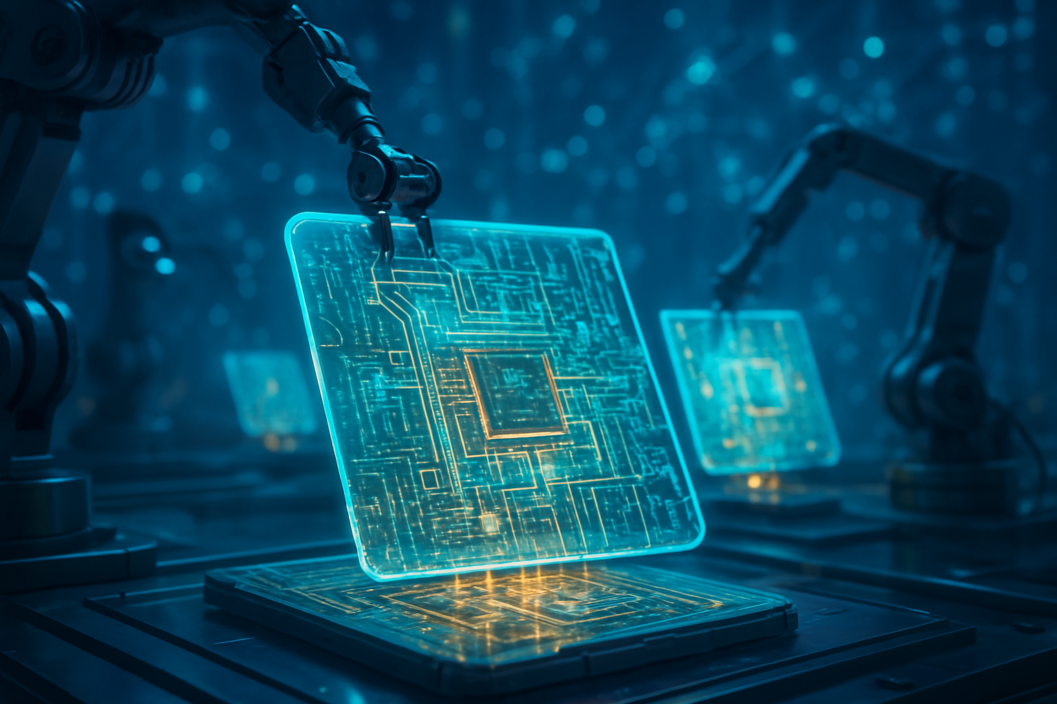
As of January 2026, the artificial intelligence industry has reached a pivotal infrastructure milestone. For the past three years, the primary bottleneck for the global AI explosion has not been the design of the chips themselves, nor the availability of raw silicon wafers, but rather the specialized "advanced packaging" required to stitch these complex processors together. TSMC (NYSE: TSM) has spent the last 24 months in a frantic race to expand its Chip-on-Wafer-on-Substrate (CoWoS) capacity, which is projected to reach an staggering 125,000 wafers per month by the end of this year—a nearly four-fold increase from early 2024 levels.
Despite this massive scale-up, the insatiable demand from hyperscalers and AI chip giants like Nvidia (NASDAQ: NVDA) and AMD (NASDAQ: AMD) has kept the capacity effectively "sold out" through 2026. This persistent supply-demand imbalance has forced a paradigm shift in semiconductor manufacturing. The industry is now rapidly transitioning from traditional circular 300mm silicon wafers to a revolutionary new format: Panel-Level Packaging (PLP). This shift, spearheaded by new technological deployments like TSMC’s CoPoS and Intel’s commercial glass substrates, represents the most significant change to chip assembly in decades, promising to break the "reticle limit" and usher in an era of massive, multi-chiplet super-processors.
Scaling Beyond the Circle: The Technical Leap to Panels
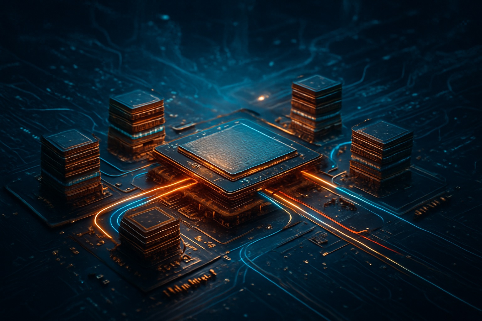
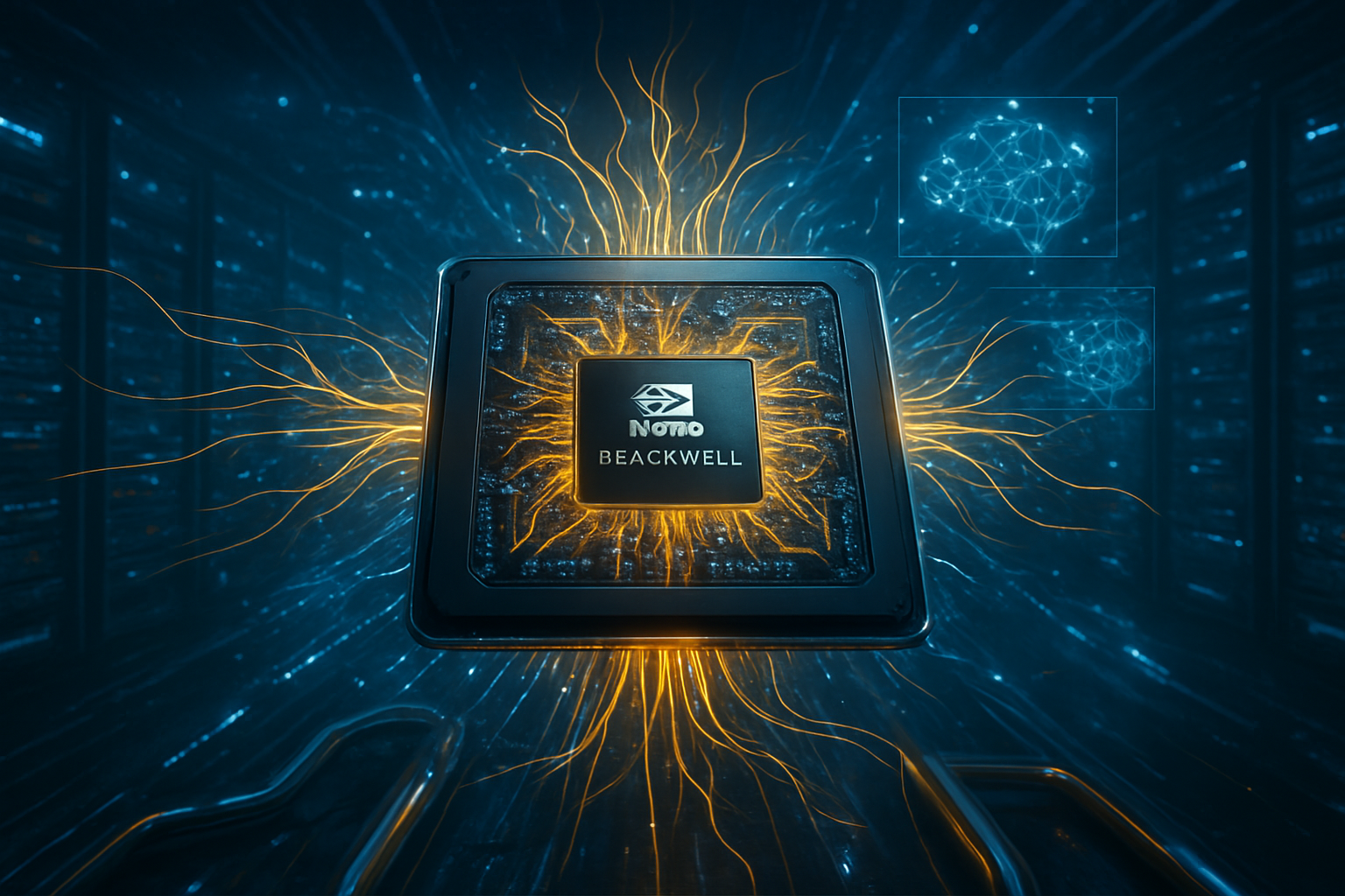
The technical limitation of current advanced packaging lies in the geometry of the wafer. Since the late 1990s, the industry standard has been the 300mm (12-inch) circular silicon wafer. However, as AI chips like Nvidia’s Blackwell and the newly announced Rubin architectures grow larger and require more High Bandwidth Memory (HBM) stacks, they are reaching the physical limits of what a circular wafer can efficiently accommodate. Panel-Level Packaging (PLP) solves this by moving from circular wafers to large rectangular panels, typically starting at 310mm x 310mm and scaling up to a massive 600mm x 600mm.
TSMC’s entry into this space, branded as CoPoS (Chip-on-Panel-on-Substrate), represents an evolution of its CoWoS technology. By using rectangular panels, manufacturers can achieve area utilization rates of over 95%, compared to the roughly 80% efficiency of circular wafers, where the edges often result in "scrap" silicon. Furthermore, the transition to glass substrates—a breakthrough Intel (NASDAQ: INTC) moved into High-Volume Manufacturing (HVM) this month—is replacing traditional organic materials. Glass offers 50% less pattern distortion and superior thermal stability, allowing for the extreme interconnect density required for the 1,000-watt AI chips currently entering the market.
Initial reactions from the AI research community have been overwhelmingly positive, as these innovations allow for "super-packages" that were previously impossible. Experts at the 2026 International Solid-State Circuits Conference (ISSCC) noted that PLP and glass substrates are the only viable path to integrating HBM4 memory, which requires twice the interconnect density of its predecessors. This transition essentially allows chipmakers to treat the packaging itself as a giant, multi-layered circuit board, effectively extending the lifespan of Moore’s Law through physical assembly rather than transistor shrinking alone.
The Competitive Scramble: Market Leaders and the OSAT Alliance
The shift to PLP has reshuffled the competitive landscape of the semiconductor industry. While TSMC remains the dominant player, securing over 60% of Nvidia's packaging orders for the next two years, the bottleneck has opened a window of opportunity for rivals. Intel has leveraged its first-mover advantage in glass substrates to position its 18A foundry services as a high-end alternative for companies seeking to avoid the TSMC backlog. Intel’s Chandler, Arizona facility is now fully operational, providing a "turnkey" advanced packaging solution on U.S. soil—a strategic advantage that has already attracted attention from defense and aerospace sectors.
Samsung (KRX: 005930) is also mounting a significant challenge through its "Triple Alliance" strategy, which integrates its display technology, electro-mechanics, and chip manufacturing arms. Samsung’s I-CubeE (Fan-Out Panel-Level Packaging) is currently being deployed to help customers like Broadcom (NASDAQ: AVGO) reduce costs by replacing expensive silicon interposers with embedded silicon bridges. This has allowed Samsung to capture a larger share of the "value-tier" AI accelerator market, providing a release valve for the high-end CoWoS shortage.
Outsourced Semiconductor Assembly and Test (OSAT) providers are also benefiting from this shift. TSMC has increasingly outsourced the "back-end" portions of the process (the "on-Substrate" part of CoWoS) to partners like ASE Technology (NYSE: ASX) and Amkor (NASDAQ: AMKR). By 2026, ASE is expected to handle nearly 45% of the back-end packaging for TSMC’s customers. This ecosystem approach has allowed the industry to scale output more rapidly than any single company could achieve alone, though it has also led to a 10-20% increase in packaging prices due to the sheer complexity of the multi-vendor supply chain.
The "Packaging Era" and the Future of AI Economics
The broader significance of the PLP transition cannot be overstated. We have moved from the "Lithography Era," where the most important factor was the size of the transistor, to the "Packaging Era," where the most important factor is the speed and density of the connection between chiplets. This shift is fundamentally changing the economics of AI. Because advanced packaging is so capital-intensive, the barrier to entry for creating high-end AI chips has skyrocketed. Only a handful of companies can afford the multi-billion dollar "entry fee" required to secure CoWoS or PLP capacity at scale.
However, there are growing concerns regarding the environmental and yield-related costs of this transition. Moving to 600mm panels requires entirely new sets of factory tools, and the early yield rates for PLP are significantly lower than those for mature 300mm wafer processes. Critics also point out that the centralization of advanced packaging in Taiwan remains a geopolitical risk, although the expansion of TSMC and Amkor into Arizona is a step toward diversification. The "warpage wall"—the tendency for large panels to bend under intense heat—remains a major engineering hurdle that companies are only now beginning to solve through the use of glass cores.
What’s Next: The Road to 2028 and the "1 Trillion Transistor" Chip
Looking ahead, the next two years will be defined by the transition from pilot lines to high-volume manufacturing for panel-level technologies. TSMC has scheduled the mass production of its CoPoS technology for late 2027 or early 2028, coinciding with the expected launch of "Post-Rubin" AI architectures. These future chips are predicted to feature "all-glass" substrates and integrated silicon photonics, allowing for light-speed data transfer between the processor and memory.
The ultimate goal, as articulated by Intel and TSMC leaders, is the "1 Trillion Transistor System-in-Package" by 2030. Achieving this will require panels even larger than today's prototypes and a complete overhaul of how we manage heat in data centers. We should expect to see a surge in "co-packaged optics" announcements in late 2026, as the electrical limits of traditional substrates finally give way to optical interconnects. The primary challenge remains yield; as chips grow larger, the probability of a single defect ruining a multi-thousand-dollar package increases exponentially.
A New Foundation for Artificial Intelligence
The resolution of the CoWoS bottleneck through the adoption of Panel-Level Packaging and glass substrates marks a definitive turning point in the history of computing. By breaking the geometric constraints of the 300mm wafer, the industry has paved the way for a new generation of AI hardware that is exponentially more powerful than the chips that fueled the initial 2023-2024 AI boom.
As we move through the first half of 2026, the key indicators of success will be the yield rates of Intel's glass substrate lines and the speed at which TSMC can bring its Chiayi AP7 facility to full capacity. While the shortage of AI compute has eased slightly due to these massive investments, the "structural demand" for intelligence suggests that packaging will remain a high-stakes battlefield for the foreseeable future. The silicon ceiling hasn't just been raised; it has been replaced by a new, rectangular, glass-bottomed foundation.
This content is intended for informational purposes only and represents analysis of current AI developments.
TokenRing AI delivers enterprise-grade solutions for multi-agent AI workflow orchestration, AI-powered development tools, and seamless remote collaboration platforms.
For more information, visit https://www.tokenring.ai/.