In a move that has sent shockwaves through both Silicon Valley and Wall Street, Amazon.com Inc. (NASDAQ: AMZN) has officially confirmed a staggering $200 billion capital expenditure plan for the 2026 fiscal year. The announcement, delivered during the company’s Q4 earnings call on February 5, 2026, marks the single largest one-year investment by a private enterprise in history. Focused heavily on a "triple-threat" strategy of AI infrastructure, custom silicon, and advanced robotics, the plan signals CEO Andy Jassy’s absolute commitment to winning what he describes as a "generational arms race" against Alphabet Inc. (NASDAQ: GOOGL) and Microsoft Corp. (NASDAQ: MSFT).
The immediate market reaction, however, was one of "sticker shock." Shares of Amazon plummeted 10% in after-hours trading and early morning sessions as investors grappled with the sheer scale of the spending. Despite AWS posting a robust 24% year-over-year revenue growth, the massive outlay has stoked fears regarding near-term margin compression and the timeline for a return on investment. Jassy remained undeterred during the call, framing the $200 billion figure not as a speculative bet, but as a necessary response to a "seminal inflection point" in the global economy.
Silicon and Steel: The Technical Core of the $200 Billion Plan
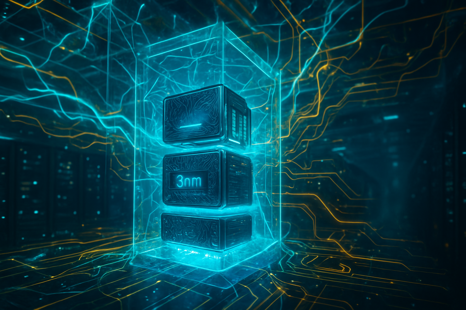
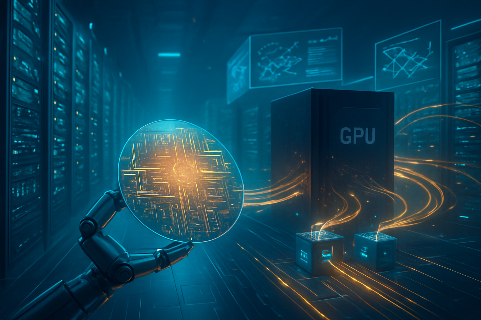
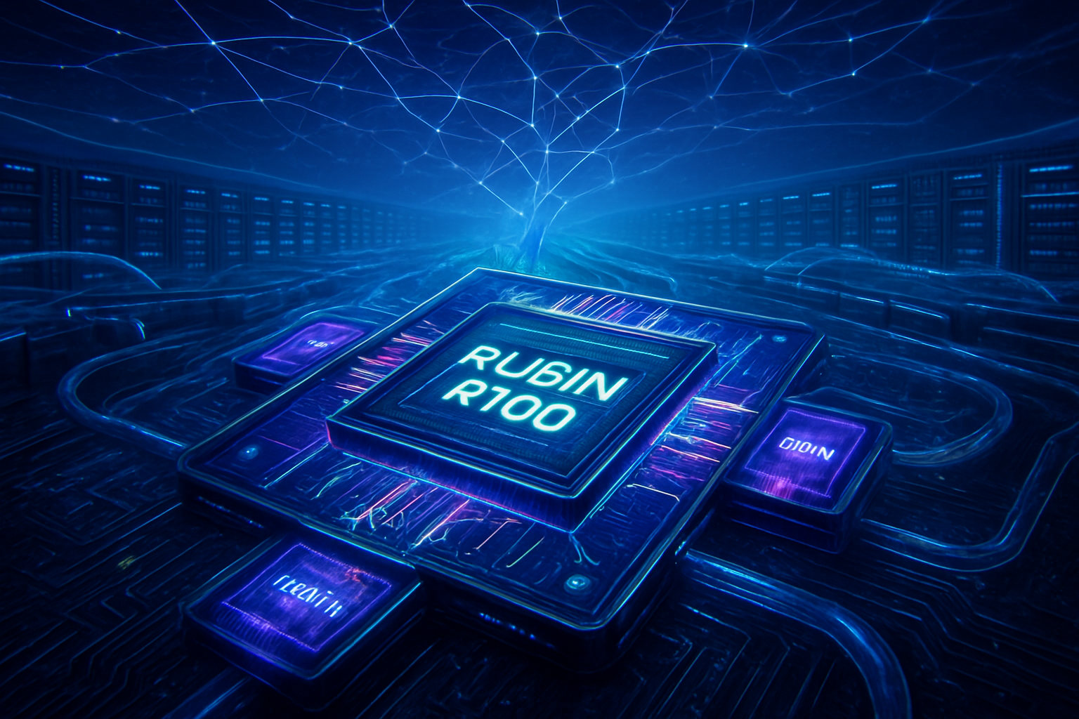
The lion’s share of the $200 billion investment is earmarked for AWS’s physical and digital foundation, with a significant pivot toward custom hardware. Central to this strategy is the general availability of Trainium 3, Amazon’s latest AI-specialized chip. Fabricated on a cutting-edge 3nm process by Taiwan Semiconductor Manufacturing Company (NYSE: TSM), Trainium 3 reportedly offers a 4.4x increase in compute performance and 4x better energy efficiency compared to its predecessor. By deploying these chips in "UltraServer" clusters capable of scaling up to one million interconnected units, Amazon aims to provide the massive compute required to train the next generation of trillion-parameter models, such as those being developed by its lead partner, Anthropic.
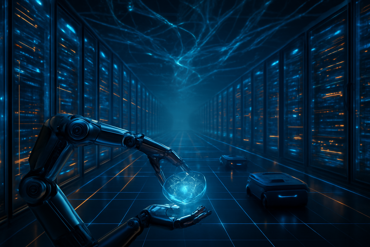
In addition to silicon, Amazon is aggressively scaling its "Physical AI" capabilities within its logistics network. The company revealed the rollout of Vulcan, a new tactile robotic arm equipped with advanced force-feedback sensors. Unlike previous iterations, Vulcan possesses a "sense of touch," allowing it to handle fragile items and pick-and-pack approximately 75% of Amazon's diverse inventory—a threshold that has long been the "holy grail" of warehouse automation. This is supported by DeepFleet AI, a generative AI orchestration layer that manages the movement of over 1.2 million autonomous robots, including the fully mobile Proteus units, across hundreds of fulfillment centers globally.
The technical shift represents a departure from the industry’s heavy reliance on Nvidia Corp. (NASDAQ: NVDA). While Amazon remains a major purchaser of Blackwell and subsequent Nvidia architectures, the $200 billion plan places a heavy emphasis on vertical integration. By designing the chips, the servers, and the robotic controllers in-house, Amazon claims it can reduce the total cost of ownership for AI workloads by up to 40%, offering a price-to-performance ratio that third-party hardware providers may struggle to match as the "arms race" intensifies.
The Cloud Hierarchy: Competitive Implications for the Big Three
Amazon's aggressive spending redefines the competitive landscape for cloud dominance. For years, Microsoft and Google have leveraged their early leads in generative AI to challenge AWS's market share. However, Jassy’s 2026 plan is an attempt to use Amazon’s massive scale to outbuild the competition. While Microsoft has leaned heavily on its partnership with OpenAI and Google has integrated Gemini across its ecosystem, Amazon is positioning itself as the "foundational layer" for all AI development. By offering the most cost-effective training environment via Trainium 3, Amazon hopes to lure startups and enterprises away from Azure and Google Cloud.
The $200 billion commitment also serves as a strategic defensive move. As Google and Microsoft continue to report multi-billion dollar capex increases, Amazon’s decision to double down ensures it will not be "out-provisioned" in the race for data center capacity. This has significant implications for AI labs; with Anthropic already scaling its workloads to nearly one million Trainium chips, Amazon is effectively securing its position as the primary host for the world’s most advanced models. This "infrastructure-first" approach may force competitors to either match the spending—further straining their own margins—or risk losing high-value enterprise clients who require guaranteed compute availability.
Furthermore, the integration of robotics gives Amazon a unique edge that its cloud-only competitors lack. While Google and Microsoft focus on digital intelligence, Amazon is applying AI to the physical world at a scale no other company can match. This dual-track strategy—leading in both virtual cloud services and physical logistics automation—creates a "flywheel" effect where gains in AI efficiency directly lower the cost of retail operations, which in turn provides more capital to reinvest in AI infrastructure.
A New Milestone in the Global AI Landscape
The scale of Amazon's 2026 plan reflects a broader shift in the AI landscape from experimentation to industrial-scale deployment. We are moving past the era of "chatbots" and entering an age where AI is a fundamental utility, akin to electricity or the internet itself. Amazon’s $200 billion bet is the largest signal to date that the tech industry views AI as the definitive backbone of future global commerce. Comparing this to previous milestones, such as the initial build-out of the 4G/5G networks or the early internet backbone, the current AI infrastructure boom is significantly more capital-intensive and concentrated among a few "hyper-scalers."
However, this massive expansion brings significant concerns, most notably regarding energy consumption and environmental impact. Building out the data center capacity to support $200 billion in hardware requires an immense amount of power. Amazon has stated it is investing heavily in small modular reactors (SMRs) and other carbon-free energy sources, but the sheer speed of the build-out has raised questions about the strain on local power grids and the company’s ability to meet its "Net Zero" commitments by 2040.
The 10% stock drop also highlights a growing tension between Silicon Valley’s long-term vision and Wall Street’s demand for quarterly discipline. There is a palpable fear that the industry is entering a "capex bubble" where the cost of building AI far outstrips the immediate revenue it generates. Jassy’s insistence that this is a "demand-led" investment will be put to the test throughout 2026. If AWS cannot maintain its 24%+ growth rate, the pressure from institutional investors to pull back on spending will become deafening.
The Horizon: What Comes Next for the AI Titan?
Looking ahead, the next 12 to 18 months will be a proving ground for Amazon’s "Physical AI" vision. The successful integration of the Vulcan tactile arms across the fulfillment network is expected to be a major catalyst for margin expansion in the retail sector, potentially offsetting the high costs of the infrastructure build-out. Experts predict that if Amazon can successfully automate 75% of its picking and stowing operations by the end of 2026, it could see a permanent 15-20% reduction in fulfillment costs, a move that would fundamentally alter the economics of e-commerce.
In the near term, all eyes will be on the performance of Trainium 3 in real-world benchmarks. If Amazon’s custom silicon can indeed outperform Nvidia’s offerings on a price-per-watt basis, we may see a significant shift in how AI models are trained. We also expect to see the "DeepFleet" orchestration model being offered as a standalone service for other logistics and manufacturing companies, potentially opening a new multibillion-dollar revenue stream for AWS in the industrial AI sector.
Challenges remain, particularly in the realm of regulatory scrutiny. As Amazon becomes the dominant provider of both the "brains" (AI chips) and the "brawn" (logistics robotics) of the modern economy, antitrust regulators in both the U.S. and E.U. are likely to take a closer look at its vertical integration. Balancing this rapid expansion with global regulatory compliance will be one of Jassy’s most difficult tasks in the coming years.
Conclusion: A Generational Bet on the Future of Intelligence
Amazon’s $200 billion capital expenditure plan for 2026 is a watershed moment in the history of technology. It is a bold, high-stakes declaration that the company intends to own the foundational infrastructure of the AI era, from the silicon wafers in the data center to the robotic fingers in the warehouse. While the 10% drop in stock price reflects immediate investor anxiety, it does little to dampen the long-term strategic trajectory set by Andy Jassy.
The significance of this development cannot be overstated; it marks the transition of AI from a software-driven innovation to a hardware-and-infrastructure-dominated industry. As the "arms race" with Google and Microsoft reaches its zenith, Amazon is betting that the company with the most efficient, most integrated, and most massive physical footprint will ultimately win. In the coming months, the performance of AWS and the successful rollout of the Vulcan robotics system will be the key metrics to watch. For now, Amazon has made its move—and it is the largest the world has ever seen.
This content is intended for informational purposes only and represents analysis of current AI developments.
TokenRing AI delivers enterprise-grade solutions for multi-agent AI workflow orchestration, AI-powered development tools, and seamless remote collaboration platforms.
For more information, visit https://www.tokenring.ai/.