Tag: Custom Silicon

  • The Silicon Sovereignty Era: Rivian’s RAP1 Chip and the High-Stakes Race for the ‘Data Center on Wheels’

    The Silicon Sovereignty Era: Rivian’s RAP1 Chip and the High-Stakes Race for the ‘Data Center on Wheels’

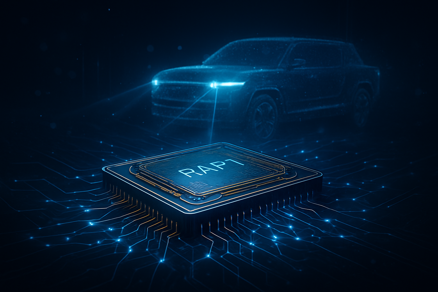
    The automotive industry has officially entered the era of "Silicon Sovereignty." As of early 2026, the battle for electric vehicle (EV) dominance is no longer being fought just on factory floors or battery chemistry labs, but within the nanometer-scale architecture of custom-designed AI chips. Leading this charge is Rivian Automotive (NASDAQ: RIVN), which recently unveiled its groundbreaking Rivian Autonomy Processor 1 (RAP1). This move signals a definitive shift away from off-the-shelf hardware toward vertically integrated, bespoke silicon designed to turn vehicles into high-performance, autonomous "data centers on wheels."

    The announcement of the RAP1 chip, which took place during Rivian’s Autonomy & AI Day in late December 2025, marks a pivotal moment for the company and the broader EV sector. By designing its own AI silicon, Rivian joins an elite group of "tech-first" automakers—including Tesla (NASDAQ: TSLA) and NIO (NYSE: NIO)—that are bypassing traditional semiconductor giants to build hardware optimized specifically for their own software stacks. This development is not merely a technical milestone; it is a strategic maneuver intended to unlock Level 4 autonomy while drastically improving vehicle range through unprecedented power efficiency.

    The technical specifications of the RAP1 chip place it at the absolute vanguard of automotive computing. Manufactured on a cutting-edge 5nm process by TSMC (NYSE: TSM) and utilizing the Armv9 architecture from Arm Holdings (NASDAQ: ARM), the RAP1 features 14 high-performance Cortex-A720AE (Automotive Enhanced) CPU cores. In its flagship configuration, the Autonomy Compute Module 3 (ACM3), Rivian pairs two RAP1 chips to deliver a staggering 1,600 sparse INT8 TOPS (Trillion Operations Per Second). This massive computational headroom is designed to process over 5 billion pixels per second, managing inputs from 11 high-resolution cameras, five radars, and a proprietary long-range LiDAR system simultaneously.

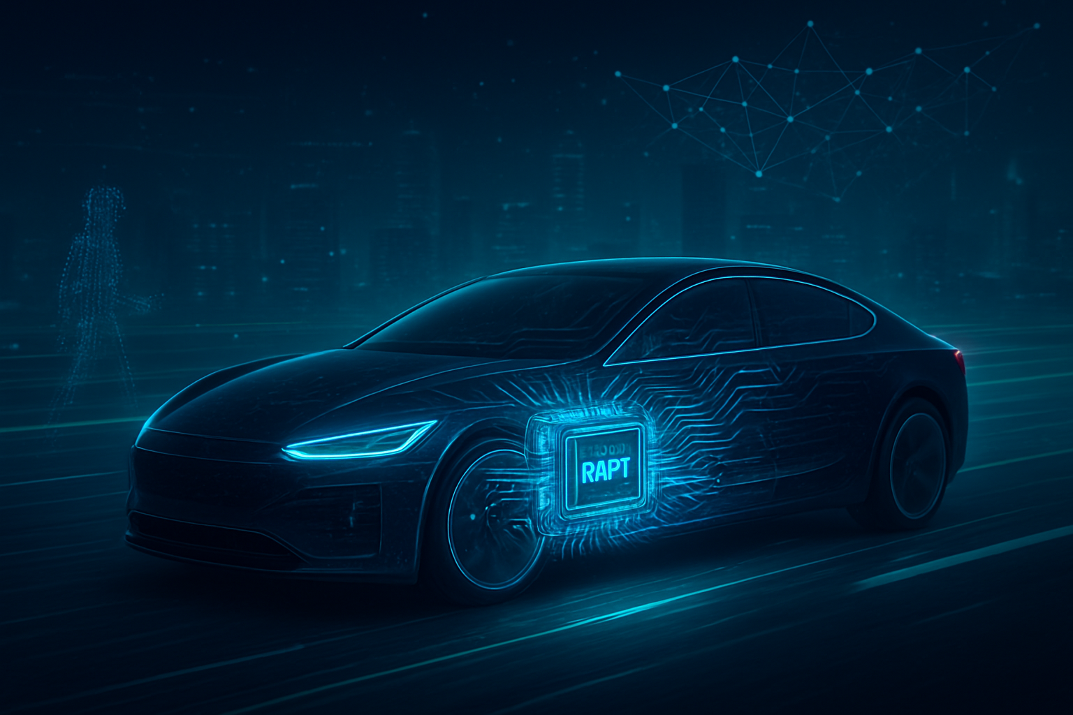
    What truly distinguishes the RAP1 from previous industry standards, such as the Nvidia (NASDAQ: NVDA) Drive Orin, is its focus on "Performance-per-Watt." Rivian claims the RAP1 is 2.5 times more power-efficient than the systems used in its second-generation vehicles. This efficiency is achieved through a specialized "RivLink" low-latency interconnect, which allows the chips to communicate with minimal overhead. The AI research community has noted that while raw TOPS were the metric of 2024, the focus in 2026 has shifted to how much intelligence can be squeezed out of every milliwatt of battery power—a critical factor for maintaining EV range during long autonomous hauls.

    Industry experts have reacted with significant interest to Rivian’s "Large Driving Model" (LDM), an end-to-end AI model that runs natively on the RAP1. Unlike legacy ADAS systems that rely on hand-coded rules, the LDM uses the RAP1’s neural processing units to predict vehicle trajectories based on massive fleet datasets. This vertical integration allows Rivian to optimize its software specifically for the RAP1’s memory bandwidth and cache hierarchy, a level of tuning that is impossible when using general-purpose silicon from third-party vendors.

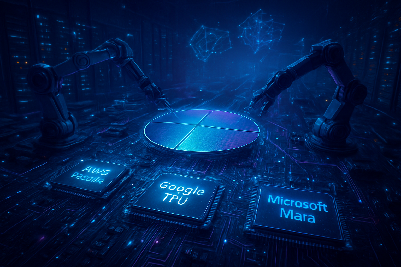
    The rise of custom automotive silicon is creating a seismic shift in the competitive landscape of the tech and auto industries. For years, Nvidia was the undisputed king of the automotive AI hill, but as companies like Rivian, NIO, and XPeng (NYSE: XPEV) transition to in-house designs, the market for high-end "merchant silicon" is facing localized disruption. While Nvidia remains a dominant force in training the AI models in the cloud, the "inference" at the edge—the actual decision-making inside the car—is increasingly moving to custom chips. This allows automakers to capture more of the value chain and eliminate the "chip tax" paid to external suppliers, with NIO estimating that its custom Shenji NX9031 chip saves the company over $1,300 per vehicle.

    Tesla remains the primary benchmark in this space, with its upcoming AI5 (Hardware 5) expected to begin sampling in early 2026. Tesla’s AI5 is rumored to be up to 40 times more performant than its predecessor, maintaining a fierce rivalry with Rivian’s RAP1 for the title of the most advanced automotive computer. Meanwhile, Chinese giants like Xiaomi (HKG: 1810) are leveraging their expertise in consumer electronics to build "Grand Convergence" platforms, where custom 3nm chips like the XRING O1 unify the car, the smartphone, and the home into a single AI-driven ecosystem.

    This trend provides a significant strategic advantage to companies that can afford the massive R&D costs of chip design. Startups and legacy automakers that lack the scale or technical expertise to design their own silicon may find themselves at a permanent disadvantage, forced to rely on generic hardware that is less efficient and more expensive. For Rivian, the RAP1 is more than a chip; it is a moat that protects its software margins and ensures that its future vehicles, such as the highly anticipated R2, are "future-proofed" for the next decade of AI advancements.

    The broader significance of the RAP1 chip lies in its role as the foundation for the "Data Center on Wheels." Modern EVs are no longer just transportation devices; they are mobile nodes in a global AI network, generating up to 5 terabytes of data per day. The transition to custom silicon allows for a "Zonal Architecture," where a single centralized compute node replaces dozens of smaller, inefficient Electronic Control Units (ECUs). This simplification reduces vehicle weight and complexity, but more importantly, it enables the deployment of Agentic AI—intelligent assistants that can proactively diagnose vehicle health, manage energy consumption, and provide natural language interaction for passengers.

    The move toward Level 4 autonomy—defined as "eyes-off, mind-off" driving in specific environments—is the ultimate goal of this silicon race. By 2026, the industry has largely moved past the "Level 2+" plateau, and the RAP1 hardware provides the necessary redundancy and compute to make Level 4 a reality in geofenced urban and highway environments. However, this progress also brings potential concerns regarding data privacy and cybersecurity. As vehicles become more reliant on centralized AI, the "attack surface" for hackers increases, necessitating the hardware-level security features that Rivian has integrated into the RAP1’s Armv9 architecture.

    Comparatively, the RAP1 represents a milestone similar to Apple’s transition to M-series silicon in its MacBooks. It is a declaration that the most important part of a modern machine is no longer the engine or the chassis, but the silicon that governs its behavior. This shift mirrors the broader AI landscape, where companies like OpenAI and Microsoft are also exploring custom silicon to optimize for specific large language models, proving that specialized hardware is the only way to keep pace with the exponential growth of AI capabilities.

    Looking ahead, the near-term focus for Rivian will be the integration of the RAP1 into the Rivian R2, scheduled for mass production in late 2026. This vehicle is expected to be the first to showcase the full potential of the RAP1’s efficiency, offering advanced Level 3 highway autonomy at a mid-market price point. In the longer term, Rivian’s roadmap points toward 2027 and 2028 for the rollout of true Level 4 features, where the RAP1’s "distributed mesh network" will allow vehicles to share real-time sensor data to "see" around corners and through obstacles.

    The next frontier for automotive silicon will likely involve even tighter integration with generative AI. Experts predict that by 2027, custom chips will include dedicated "Transformer Engines" designed specifically to accelerate the attention mechanisms used in Large Language Models and Vision Transformers. This will enable cars to not only navigate the world but to understand it contextually—recognizing the difference between a child chasing a ball and a pedestrian standing on a sidewalk. The challenge will be managing the thermal output of these massive processors while maintaining the ultra-low latency required for safety-critical driving decisions.

    The unveiling of the Rivian RAP1 chip is a watershed moment in the history of automotive technology. It signifies the end of the era where car companies were simply assemblers of parts and the beginning of an era where they are the architects of the most sophisticated AI hardware on the planet. The RAP1 is a testament to the "data center on wheels" philosophy, proving that the path to Level 4 autonomy and maximum EV efficiency runs directly through custom silicon.

    As we move through 2026, the industry will be watching closely to see how the RAP1 performs in real-world conditions and how quickly Rivian can scale its production. The success of this chip will likely determine Rivian’s standing in the high-stakes EV market and may serve as a blueprint for other manufacturers looking to reclaim their "Silicon Sovereignty." For now, the RAP1 stands as a powerful symbol of the convergence between the automotive and AI industries—a convergence that is fundamentally redefining what it means to drive.


    This content is intended for informational purposes only and represents analysis of current AI developments.

    TokenRing AI delivers enterprise-grade solutions for multi-agent AI workflow orchestration, AI-powered development tools, and seamless remote collaboration platforms.
    For more information, visit https://www.tokenring.ai/.

  • The Silicon Divorce: Hyperscalers Launch Custom AI Chips to Break NVIDIA’s Monopoly

    The Silicon Divorce: Hyperscalers Launch Custom AI Chips to Break NVIDIA’s Monopoly

    As the calendar turns to early 2026, the artificial intelligence industry is witnessing its most significant infrastructure shift since the start of the generative AI boom. For years, the "NVIDIA tax"—the high cost and limited supply of high-end GPUs—has been the primary bottleneck for tech giants. Today, that era of total dependence is coming to a close. Google, a subsidiary of Alphabet Inc. (NASDAQ: GOOGL), and Meta Platforms, Inc. (NASDAQ: META), have officially moved their latest generations of custom silicon, the TPU v6 (Trillium) and MTIA v3, into mass production, signaling a major transition toward vertical integration in the cloud.

    This movement represents more than just a search for cost savings; it is a fundamental architectural pivot. By designing chips specifically for their own internal workloads—such as recommendation algorithms, large language model (LLM) inference, and massive-scale training—hyperscalers are achieving performance-per-watt efficiencies that general-purpose GPUs struggle to match. As these custom accelerators flood data centers throughout 2026, the competitive landscape for AI infrastructure is being rewritten, challenging the long-standing dominance of NVIDIA (NASDAQ: NVDA) in the enterprise cloud.

    Technical Prowess: The Rise of Specialized ASICs

    The Google TPU v6, codenamed Trillium, has entered 2026 as the volume leader in Google’s fleet, with production scaling to over 1.6 million units this year. Trillium represents a massive leap forward, boasting a 4.7x increase in peak compute performance per chip compared to its predecessor, the TPU v5e. Technically, the TPU v6 is optimized for the "SparseCore" architecture, which is critical for the massive embedding tables used in modern recommendation systems and the "Mixture of Experts" (MoE) models that power the latest iterations of Gemini. By doubling the High Bandwidth Memory (HBM) capacity and bandwidth, Google has created a chip that excels at the high-throughput demands of 2026’s multimodal AI agents.

    Simultaneously, Meta’s MTIA v3 (Meta Training and Inference Accelerator) has moved from testing into full-scale deployment. Unlike earlier versions which were primarily focused on inference, the MTIA v3 is a full-stack training and inference solution. Built on a refined 3nm process, the MTIA v3 utilizes a custom RISC-V-based matrix compute grid. This architecture is specifically tuned to run Meta’s PyTorch-based workloads with surgical precision. Early benchmarks suggest that the MTIA v3 provides a 3x performance boost over its predecessor, allowing Meta to train its Llama-series models with significantly lower latency and power consumption than standard GPU clusters.

    This shift differs from previous approaches because it moves away from the "one-size-fits-all" philosophy of the GPU. While NVIDIA’s Blackwell architecture remains the gold standard for raw, versatile power, the TPU v6 and MTIA v3 are Application-Specific Integrated Circuits (ASICs). They strip away the hardware overhead required for general-purpose graphics or scientific simulation, focusing entirely on the tensor operations and memory management required for neural networks. Industry experts have noted that while a GPU is a "Swiss Army knife," these new chips are high-precision scalpels, designed to perform specific AI tasks with nearly double the cost-efficiency of general hardware.

    The reaction from the AI research community has been one of cautious optimism. Researchers at major labs have highlighted that the proliferation of custom silicon is finally easing the "compute crunch" that defined 2024 and 2025. However, the transition has required a significant software evolution. The success of these chips in 2026 is largely attributed to the maturity of open-source compilers like OpenAI’s Triton and the release of PyTorch 3.0, which have effectively neutralized NVIDIA's "CUDA moat" by making it easier for developers to port code across different hardware architectures without massive performance penalties.

    Market Repercussions: Challenging the NVIDIA Hegemony

    The strategic implications for the tech giants are profound. For companies like Google and Meta, producing their own silicon is a defensive necessity. By 2026, inference workloads—the process of running a trained model for users—are projected to account for nearly 70% of all AI-related compute. Because custom ASICs like the TPU v6 are roughly 1.4x to 2x more cost-efficient than GPUs for inference, Google can offer its AI services at a lower price point than competitors who are still paying a premium for third-party hardware. This vertical integration provides a massive margin advantage in the increasingly commoditized market for LLM API calls.

    NVIDIA is already feeling the pressure. While the company still maintains a commanding lead in the highest-end frontier model training, its market share in the broader AI accelerator space is expected to slip from its peak of 95% down toward 75-80% by the end of 2026. The rise of "Hyperscaler Silicon" means that Amazon.com, Inc. (NASDAQ: AMZN) and Microsoft Corporation (NASDAQ: MSFT) are also less reliant on NVIDIA’s roadmap. Amazon’s Trainium 3 (Trn3) has also reached mass deployment this year, achieving performance parity with NVIDIA’s Blackwell racks for specific training tasks, further crowding the high-end market.

    For startups and smaller AI labs, this development is a double-edged sword. On one hand, the increased competition is driving down the cost of cloud compute, making it cheaper to build and deploy new models. On the other hand, the best-performing hardware is increasingly "walled off" within specific cloud ecosystems. A startup using Google Cloud may find that their models run significantly faster on TPU v6, but moving those same models to Microsoft Azure’s Maia 200 silicon could require significant re-optimization. This creates a new kind of "vendor lock-in" based on hardware architecture rather than just software APIs.

    Strategic positioning in 2026 is now defined by "silicon sovereignty." Meta, for instance, has stated its goal to migrate 100% of its internal recommendation traffic to MTIA by 2027. By owning the hardware, Meta can optimize its social media algorithms at a level of granularity that was previously impossible. This allows for more complex, real-time personalization of content without a corresponding explosion in data center energy costs, giving Meta a distinct advantage in the battle for user attention and advertising efficiency.

    The Industrialization of AI

    The shift toward custom silicon in 2026 marks the "industrialization phase" of the AI revolution. In the early days, the industry relied on whatever hardware was available—primarily gaming GPUs. Today, the infrastructure is being purpose-built for the task at hand. This mirrors historical trends in other industries, such as the transition from general-purpose steam engines to specialized internal combustion engines designed for specific types of vehicles. It signifies that AI has moved from a research curiosity to the foundational utility of the modern economy.

    Environmental concerns are also a major driver of this trend. As global energy grids struggle to keep up with the demands of massive data centers, the efficiency gains of chips like the TPU v6 are critical. Custom silicon allows hyperscalers to do more with less power, which is essential for meeting the sustainability targets that many of these corporations have set for the end of the decade. The ability to perform 4.7x more compute per watt isn't just a financial metric; it's a regulatory and social necessity in a world increasingly conscious of the carbon footprint of digital services.

    However, this transition also raises concerns about the concentration of power. As the "Big Five" tech companies develop their own proprietary hardware, the barrier to entry for a new cloud provider becomes nearly insurmountable. It is no longer enough to buy a fleet of GPUs; a competitor would now need to invest billions in R&D to design their own chips just to achieve price parity. This could lead to a permanent oligopoly in the AI infrastructure space, where only a handful of companies possess the specialized hardware required to run the world's most advanced intelligence systems.

    Comparatively, this milestone is being viewed as the "Post-GPU Era." While GPUs will likely always have a place in the market due to their versatility and the massive ecosystem surrounding them, they are no longer the undisputed kings of the data center. The successful mass production of TPU v6 and MTIA v3 in 2026 serves as a clear signal that the future of AI is heterogeneous. We are moving toward a world where the hardware is as specialized as the software it runs, leading to a more efficient, albeit more fragmented, technological landscape.

    The Road to 2027 and Beyond

    Looking ahead, the silicon wars are only expected to intensify. Even as TPU v6 and MTIA v3 dominate the headlines today, Google is already beginning the limited rollout of TPU v7 (Ironwood), its first 3nm chip designed for massive rack-scale computing. Experts predict that by 2027, we will see the first 2nm AI chips entering the prototyping phase, pushing the limits of Moore’s Law even further. The focus will likely shift from raw compute power to "interconnect density"—how fast these thousands of custom chips can talk to one another to form a single, giant "planetary computer."

    We also expect to see these custom designs move closer to the "edge." While 2026 is the year of the data center chip, the architectural lessons learned from MTIA and TPU are already being applied to mobile processors and local AI accelerators. This will eventually lead to a seamless continuum of AI hardware, where a model can be trained on a TPU v6 cluster and then deployed on a specialized mobile NPU (Neural Processing Unit) that shares the same underlying architecture, ensuring maximum efficiency from the cloud to the pocket.

    The primary challenge moving forward will be the talent war. Designing world-class silicon requires a highly specialized workforce of chip architects and physical design engineers. As hyperscalers continue to expand their hardware divisions, the competition for this talent will be fierce. Furthermore, the geopolitical stability of the semiconductor supply chain remains a lingering concern. While Google and Meta design their chips in-house, they still rely on foundries like TSMC for production. Any disruption in the global supply chain could stall the ambitious rollout plans for 2027 and beyond.

    Conclusion: A New Era of Infrastructure

    The mass production of Google’s TPU v6 and Meta’s MTIA v3 in early 2026 represents a pivotal moment in the history of computing. It marks the end of NVIDIA’s absolute monopoly and the beginning of a new era of vertical integration and specialized hardware. By taking control of their own silicon, hyperscalers are not only reducing costs but are also unlocking new levels of performance that will define the next generation of AI applications.

    In terms of significance, 2026 will be remembered as the year the "AI infrastructure stack" was finally decoupled from the gaming GPU heritage. The move to ASICs represents a maturation of the field, where efficiency and specialization are the new metrics of success. This development ensures that the rapid pace of AI advancement can continue even as the physical and economic limits of general-purpose hardware are reached.

    In the coming months, the industry will be watching closely to see how NVIDIA responds with its upcoming Vera Rubin (R100) architecture and how quickly other players like Microsoft and AWS can scale their own designs. The battle for the heart of the AI data center is no longer just about who has the most chips, but who has the smartest ones. The silicon divorce is finalized, and the future of intelligence is now being forged in custom-designed silicon.


    This content is intended for informational purposes only and represents analysis of current AI developments.

    TokenRing AI delivers enterprise-grade solutions for multi-agent AI workflow orchestration, AI-powered development tools, and seamless remote collaboration platforms.
    For more information, visit https://www.tokenring.ai/.

  • The Great Decoupling: How Hyperscalers are Breaking NVIDIA’s Iron Grip with Custom Silicon

    The Great Decoupling: How Hyperscalers are Breaking NVIDIA’s Iron Grip with Custom Silicon

    The era of the general-purpose AI chip is rapidly giving way to a new age of hyper-specialization. As of early 2026, the world’s largest cloud providers—Google (NASDAQ:GOOGL), Amazon (NASDAQ:AMZN), and Microsoft (NASDAQ:MSFT)—have fundamentally rewritten the rules of the AI infrastructure market. By designing their own custom silicon, these "hyperscalers" are no longer just customers of the semiconductor industry; they are its most formidable architects. This strategic shift, often referred to as the "Silicon Divorce," marks a pivotal moment where the software giants have realized that to own the future of artificial intelligence, they must first own the atoms that power it.

    The immediate significance of this transition cannot be overstated. By moving away from a one-size-fits-all hardware model, these companies are slashing the astronomical "NVIDIA tax," reducing energy consumption in an increasingly power-constrained world, and optimizing their hardware for the specific nuances of their multi-trillion-parameter models. This vertical integration—controlling everything from the power source to the chip architecture to the final AI agent—is creating a competitive moat that is becoming nearly impossible for smaller players to cross.

    The Rise of the AI ASIC: Technical Frontiers of 2026

    The technical landscape of 2026 is dominated by Application-Specific Integrated Circuits (ASICs) that leave traditional GPUs in the rearview mirror for specific AI tasks. Google’s latest offering, the TPU v7 (codenamed "Ironwood"), represents the pinnacle of this evolution. Utilizing a cutting-edge 3nm process from TSMC, the TPU v7 delivers a staggering 4.6 PFLOPS of dense FP8 compute per chip. Unlike general-purpose GPUs, Google uses Optical Circuit Switching (OCS) to dynamically reconfigure its "Superpods," allowing for 10x faster collective operations than equivalent Ethernet-based clusters. This architecture is specifically tuned for the massive KV-caches required for the long-context windows of Gemini 2.0 and beyond.

    Amazon has followed a similar path with its Trainium3 chip, which entered volume production in early 2026. Designed by Amazon’s Annapurna Labs, Trainium3 is the company's first 3nm-class chip, offering 2.5 PFLOPS of MXFP8 performance. Amazon’s strategy focuses on "price-performance," leveraging the Neuron SDK to allow developers to seamlessly switch from NVIDIA (NASDAQ:NVDA) hardware to custom silicon. Meanwhile, Microsoft has solidified its position with the Maia 2 (Braga) accelerator. While Maia 100 was a conservative first step, Maia 2 is a vertically integrated powerhouse designed specifically to run Azure OpenAI services like GPT-5 and Microsoft Copilot with maximum efficiency, utilizing custom Ethernet-based interconnects to bypass traditional networking bottlenecks.

    These advancements differ from previous approaches by stripping away legacy hardware components—such as graphics rendering units and 64-bit precision—that are unnecessary for AI workloads. This "lean" architecture allows for significantly higher transistor density dedicated solely to matrix multiplications. Initial reactions from the research community have been overwhelmingly positive, with many noting that the specialized memory hierarchies of these chips are the only reason we have been able to scale context windows into the tens of millions of tokens without a total collapse in inference speed.

    The Strategic Divorce: A New Power Dynamic in Silicon Valley

    This shift has created a seismic ripple across the tech industry, benefiting a new class of "silent partners." While the hyperscalers design the chips, they rely on specialized design firms like Broadcom (NASDAQ:AVGO) and Marvell (NASDAQ:MRVL) to bring them to life. Broadcom, which now commands nearly 70% of the custom AI ASIC market, has become the backbone of the "Silicon Divorce," serving as the primary design partner for both Google and Meta (NASDAQ:META). Marvell has similarly positioned itself as a "growth challenger," securing massive wins with Amazon and Microsoft by integrating advanced "Photonic Fabrics" that allow for ultra-fast chip-to-chip communication.

    For NVIDIA, the competitive implications are complex. While the company remains the market leader with its newly launched Vera Rubin architecture, it is no longer the only game in town. The "NVIDIA Tax"—the high margins associated with the H100 and B200 series—is being eroded by the hyperscalers' internal alternatives. In response, cloud pricing has shifted to a two-tier model. Hyperscalers now offer their internal chips at a 30% to 50% discount compared to NVIDIA-based instances, effectively using their custom silicon as a loss leader to lock enterprises into their respective cloud ecosystems.

    Startups and smaller AI labs are the unexpected beneficiaries of this hardware war. The increased availability of lower-cost, high-performance compute on platforms like AWS Trainium and Google TPU v7 has lowered the barrier to entry for training mid-sized foundation models. However, the strategic advantage remains with the giants; by co-designing the hardware and the software (such as Google’s XLA compiler or Amazon’s Triton integration), these companies can squeeze performance out of their chips that no third-party user can ever hope to replicate on generic hardware.

    The Power Wall and the Quest for Energy Sovereignty

    Beyond the boardroom battles, the move toward custom silicon is driven by a looming physical reality: the "Power Wall." As of 2026, the primary constraint on AI scaling is no longer the number of chips, but the availability of electricity. Global data center power consumption is projected to reach record highs this year, and custom ASICs are the primary weapon against this energy crisis. By offering 30% to 40% better power efficiency than general-purpose GPUs, chips like the TPU v7 and Trainium3 allow hyperscalers to pack more compute into the same power envelope.

    This has led to the rise of "Sovereign AI" and a trend toward total vertical integration. We are seeing the emergence of "AI Factories"—massive, multi-billion-dollar campuses where the data center is co-located with its own dedicated power source. Microsoft’s involvement in "Project Stargate" and Google’s investments in Small Modular Reactors (SMRs) are prime examples of this trend. The goal is no longer just to build a better chip, but to build a vertically integrated supply chain of intelligence that is immune to geopolitical shifts or energy shortages.

    This movement mirrors previous milestones in computing history, such as the shift from mainframes to x86 architecture, but on a much more massive scale. The concern, however, is the "closed" nature of these ecosystems. Unlike the open standards of the PC era, the custom silicon era is highly proprietary. If the best AI performance can only be found inside the walled gardens of Azure, GCP, or AWS, the dream of a decentralized and open AI landscape may become increasingly difficult to realize.

    The Frontier of 2027: Photonics and 2nm Nodes

    Looking ahead, the next frontier for custom silicon lies in light-based computing and even smaller process nodes. TSMC has already begun ramping up 2nm (N2) mass production for the 2027 chip cycle, which will utilize Gate-All-Around (GAAFET) transistors to provide another leap in efficiency. Experts predict that the next generation of chips—Google’s TPU v8 and Amazon’s Trainium4—will likely be the first to move entirely to 2nm, potentially doubling the performance-per-watt once again.

    Furthermore, "Silicon Photonics" is moving from the lab to the data center. Companies like Marvell are already testing "Photonic Compute Units" that perform matrix multiplications using light rather than electricity, promising a 100x efficiency gain for specific inference tasks by the end of the decade. The challenge will be managing the heat; liquid cooling has already become the baseline for AI data centers in 2026, but the next generation of chips may require even more exotic solutions, such as microfluidic cooling integrated directly into the silicon substrate.

    As AI models continue to grow toward the "Quadrillion Parameter" mark, the industry will likely see a further bifurcation between "Training Monsters"—massive, liquid-cooled clusters of custom ASICs—and "Edge Inference" chips designed to run sophisticated models on local devices. The next 24 months will be defined by how quickly these hyperscalers can scale their 3nm production and whether NVIDIA's Rubin architecture can offer enough of a performance leap to justify its premium price tag.

    Conclusion: A New Foundation for the Intelligence Age

    The transition to custom silicon by Google, Amazon, and Microsoft marks the end of the "one size fits all" era of AI compute. By January 2026, the success of these internal hardware programs has proven that the most efficient way to process intelligence is through specialized, vertically integrated stacks. This development is as significant to the AI age as the development of the microprocessor was to the personal computing revolution, signaling a shift from experimental scaling to industrial-grade infrastructure.

    The key takeaway for the industry is clear: hardware is no longer a commodity; it is a core competency. In the coming months, observers should watch for the first benchmarks of the TPU v7 in "Gemini 3" training and the potential announcement of OpenAI’s first fully independent silicon efforts. As the "Silicon Divorce" matures, the gap between those who own their hardware and those who rent it will only continue to widen, fundamentally reshaping the power structure of the global technology landscape.


    This content is intended for informational purposes only and represents analysis of current AI developments.

    TokenRing AI delivers enterprise-grade solutions for multi-agent AI workflow orchestration, AI-powered development tools, and seamless remote collaboration platforms.
    For more information, visit https://www.tokenring.ai/.

  • The Great Silicon Divorce: How Cloud Giants Are Breaking Nvidia’s Iron Grip on AI

    The Great Silicon Divorce: How Cloud Giants Are Breaking Nvidia’s Iron Grip on AI

    As we enter 2026, the artificial intelligence industry is witnessing a tectonic shift in its power dynamics. For years, Nvidia (NASDAQ: NVDA) has enjoyed a near-monopoly on the high-performance hardware required to train and deploy large language models. However, the era of "Silicon Sovereignty" has arrived. The world’s largest cloud hyperscalers—Amazon (NASDAQ: AMZN), Google (NASDAQ: GOOGL), and Microsoft (NASDAQ: MSFT)—are no longer content being Nvidia's largest customers; they have become its most formidable architectural rivals. By developing custom AI silicon like Trainium, TPU v7, and Maia, these tech titans are systematically reducing their reliance on the GPU giant to slash costs and optimize performance for their proprietary models.

    The immediate significance of this shift is most visible in the bottom line. With AI infrastructure spending reaching record highs—Microsoft’s CAPEX alone hit a staggering $80 billion last year—the "Nvidia Tax" has become a burden too heavy to bear. By designing their own chips, hyperscalers are achieving a "Sovereignty Dividend," reporting a 30% to 40% reduction in total cost of ownership (TCO). This transition marks the end of the general-purpose GPU’s absolute reign and the beginning of a fragmented, specialized hardware landscape where the software and the silicon are co-engineered for maximum efficiency.

    The Rise of Custom Architectures: TPU v7, Trainium3, and Maia 200

    The technical specifications of the latest custom silicon reveal a narrowing gap between specialized ASICs (Application-Specific Integrated Circuits) and Nvidia’s flagship GPUs. Google’s TPU v7, codenamed "Ironwood," has emerged as a powerhouse in early 2026. Built on a cutting-edge 3nm process, the TPU v7 matches Nvidia’s Blackwell B200 in raw FP8 compute performance, delivering 4.6 PFLOPS. Google has integrated these chips into massive "pods" of 9,216 units, utilizing an Optical Circuit Switch (OCS) that allows the entire cluster to function as a single 42-exaflop supercomputer. Google now reports that over 75% of its Gemini model computations are handled by its internal TPU fleet, a move that has significantly insulated the company from supply chain volatility.

    Amazon Web Services (AWS) has followed suit with the general availability of Trainium3, announced at re:Invent 2025. Trainium3 offers a 2x performance boost over its predecessor and is 4x more energy-efficient, serving as the backbone for "Project Rainier," a massive compute cluster dedicated to Anthropic. Meanwhile, Microsoft is ramping up production of its Maia 200 (Braga) chip. While Maia has faced production delays and currently trails Nvidia’s raw power, Microsoft is leveraging its "MX" data format and advanced liquid-cooled infrastructure to optimize the chip for Azure’s specific AI workloads. These custom chips differ from traditional GPUs by stripping away legacy graphics-processing circuitry, focusing entirely on the dense matrix multiplication required for transformer-based models.

    Strategic Realignment: Winners, Losers, and the Shadow Giants

    This shift toward vertical integration is fundamentally altering the competitive landscape. For the hyperscalers, the strategic advantage is clear: they can now offer AI compute at prices that Nvidia-based competitors cannot match. In early 2026, AWS implemented a 45% price cut on its Nvidia-based instances, a move widely interpreted as a defensive strategy to keep customers within its ecosystem while it scales up its Trainium and Inferentia offerings. This pricing pressure forces a difficult choice for startups and AI labs: pay a premium for the flexibility of Nvidia’s CUDA ecosystem or migrate to custom silicon for significantly lower operational costs.

    While Nvidia remains the dominant force with roughly 90% of the data center GPU market, the "shadow winners" of this transition are the silicon design partners. Broadcom (NASDAQ: AVGO) and Marvell (NASDAQ: MRVL) have become the primary enablers of the custom chip revolution. Broadcom’s AI revenue is projected to reach $46 billion in 2026, driven largely by its role in co-designing Google’s TPUs and Meta’s (NASDAQ: META) MTIA chips. These companies provide the essential intellectual property and design expertise that allow software giants to become hardware manufacturers overnight, effectively commoditizing the silicon layer of the AI stack.

    The Great Inference Shift and the Sovereignty Dividend

    The broader AI landscape is currently defined by a pivot from training to inference. In 2026, an estimated 70% of all AI workloads are inference-related—the process of running a pre-trained model to generate responses. This is where custom silicon truly shines. While training a frontier model still often requires the raw, flexible power of an Nvidia cluster, the repetitive, high-volume nature of inference is perfectly suited for cost-optimized ASICs. Chips like AWS Inferentia and Meta’s MTIA are designed to maximize "tokens per watt," a metric that has become more important than raw FLOPS for companies operating at a global scale.

    This development mirrors previous milestones in computing history, such as the transition from mainframes to distributed cloud computing. Just as the cloud allowed companies to move away from expensive, proprietary hardware toward scalable, utility-based services, custom AI silicon is democratizing access to high-scale inference. However, this trend also raises concerns about "ecosystem lock-in." As hyperscalers optimize their software stacks for their own silicon, moving a model from Google Cloud to Azure or AWS becomes increasingly complex, potentially stifling the interoperability that the open-source AI community has fought to maintain.

    The Future of Silicon: Nvidia’s Rubin and Hybrid Ecosystems

    Looking ahead, the battle for silicon supremacy is only intensifying. In response to the custom chip threat, Nvidia used CES 2026 to launch its "Vera Rubin" architecture. Named after the pioneering astronomer, the Rubin platform utilizes HBM4 memory and a 3nm process to deliver unprecedented efficiency. Nvidia’s strategy is to make its general-purpose GPUs so efficient that the marginal cost savings of custom silicon become negligible for third-party developers. Furthermore, the upcoming Trainium4 from AWS suggests a future of "hybrid environments," featuring support for Nvidia NVLink Fusion. This will allow custom silicon to sit directly inside Nvidia-designed racks, enabling a mix-and-match approach to compute.

    Experts predict that the next two years will see a "tiering" of the AI hardware market. High-end frontier model training will likely remain the domain of Nvidia’s most advanced GPUs, while the vast majority of mid-tier training and global inference will migrate to custom ASICs. The challenge for hyperscalers will be to build software ecosystems that can rival Nvidia’s CUDA, which remains the industry standard for AI development. If the cloud giants can simplify the developer experience for their custom chips, Nvidia’s iron grip on the market may finally be loosened.

    Conclusion: A New Era of AI Infrastructure

    The rise of custom AI silicon represents one of the most significant shifts in the history of computing. We have moved beyond the "gold rush" phase where any available GPU was a precious commodity, into a sophisticated era of specialized, cost-effective infrastructure. The aggressive moves by Amazon, Google, and Microsoft to build their own chips are not just about saving money; they are about securing their future in an AI-driven world where compute is the most valuable resource.

    In the coming months, the industry will be watching the deployment of Nvidia’s Rubin architecture and the performance benchmarks of Microsoft’s Maia 200. As the "Silicon Sovereignty" movement matures, the ultimate winners will be the enterprises and developers who can leverage this new diversity of hardware to build more powerful, efficient, and accessible AI applications. The great silicon divorce is underway, and the AI landscape will never be the same.


    This content is intended for informational purposes only and represents analysis of current AI developments.

    TokenRing AI delivers enterprise-grade solutions for multi-agent AI workflow orchestration, AI-powered development tools, and seamless remote collaboration platforms.
    For more information, visit https://www.tokenring.ai/.

  • The $2,000 Vehicle: Rivian’s RAP1 AI Chip and the Era of Custom Automotive Silicon

    The $2,000 Vehicle: Rivian’s RAP1 AI Chip and the Era of Custom Automotive Silicon

    In a move that solidifies its position as a frontrunner in the "Silicon Sovereignty" movement, Rivian Automotive, Inc. (NASDAQ: RIVN) recently unveiled its first proprietary AI processor, the Rivian Autonomy Processor 1 (RAP1). Announced during the company’s Autonomy & AI Day in late 2025, the RAP1 marks a decisive departure from third-party hardware providers. By designing its own silicon, Rivian is not just building a car; it is building a specialized supercomputer on wheels, optimized for the unique demands of "physical AI" and real-world sensor fusion.

    The announcement centers on a strategic shift toward vertical integration that aims to drastically reduce the cost of autonomous driving technology. Dubbed by some industry insiders as the push toward the "$2,000 Vehicle" hardware stack, Rivian’s custom silicon strategy targets a 30% reduction in the bill of materials (BOM) for its autonomy systems. This efficiency allows Rivian to offer advanced driver-assistance features at a fraction of the price of its competitors, effectively democratizing high-level autonomy for the mass market.

    Technical Prowess: The RAP1 and ACM3 Architecture

    The RAP1 is a technical marvel fabricated on the 5nm process from Taiwan Semiconductor Manufacturing Company (NYSE: TSM). Built using the Armv9 architecture from Arm Holdings plc (NASDAQ: ARM), the chip features 14 Cortex-A720AE cores specifically designed for automotive safety and ASIL-D compliance. What sets the RAP1 apart is its raw AI throughput; a single chip delivers between 1,600 and 1,800 sparse INT8 TOPS (Trillion Operations Per Second). In its flagship Autonomy Compute Module 3 (ACM3), Rivian utilizes dual RAP1 chips, allowing the vehicle to process over 5 billion pixels per second with unprecedented low latency.

    Unlike general-purpose chips from NVIDIA Corporation (NASDAQ: NVDA) or Qualcomm Incorporated (NASDAQ: QCOM), the RAP1 is architected specifically for "Large Driving Models" (LDM). These end-to-end neural networks require massive data bandwidth to handle simultaneous inputs from cameras, Radar, and LiDAR. Rivian’s custom "RivLink" interconnect enables these dual chips to function as a single, cohesive unit, providing linear scaling for future software updates. This hardware-level optimization allows the RAP1 to be 2.5 times more power-efficient than previous-generation setups while delivering four times the performance.

    The research community has noted that Rivian’s approach differs significantly from Tesla, Inc. (NASDAQ: TSLA), which has famously eschewed LiDAR in favor of a vision-only system. The RAP1 includes dedicated hardware acceleration for "unstructured point cloud" data, making it uniquely capable of processing LiDAR information natively. This hybrid approach—combining the depth perception of LiDAR with the semantic understanding of high-resolution cameras—is seen by many experts as a more robust path to true Level 4 autonomous driving in complex urban environments.

    Disrupting the Silicon Status Quo

    The introduction of the RAP1 creates a significant shift in the competitive landscape of both the automotive and semiconductor industries. For years, NVIDIA and Qualcomm have dominated the "brains" of the modern EV. However, as companies like Rivian, Nio Inc. (NYSE: NIO), and XPeng Inc. (NYSE: XPEV) follow Tesla’s lead in designing custom silicon, the market for general-purpose automotive chips is facing a "hollowing out" at the high end. Rivian’s move suggests that for a premium EV maker to survive, it must own its compute stack to avoid the "vendor margin" that inflates vehicle prices.

    Strategically, this vertical integration gives Rivian a massive advantage in pricing power. By cutting out the middleman, Rivian has priced its "Autonomy+" package at a one-time fee of $2,500—significantly lower than Tesla’s Full Self-Driving (FSD) suite. This aggressive pricing is intended to drive high take-rates for the upcoming R2 and R3 platforms, creating a recurring revenue stream through software services that would be impossible if the hardware costs remained prohibitively high.

    Furthermore, this development puts pressure on traditional "Legacy" automakers who still rely on Tier 1 suppliers for their electronics. While companies like Ford or GM may struggle to transition to in-house chip design, Rivian’s success with the RAP1 demonstrates that a smaller, more agile tech-focused automaker can successfully compete with silicon giants. The strategic advantage of having hardware that is perfectly "right-sized" for the software it runs cannot be overstated, as it leads to better thermal management, lower power consumption, and longer battery range.

    The Broader Significance: Physical AI and Safety

    The RAP1 announcement is more than just a hardware update; it represents a milestone in the evolution of "Physical AI." While generative AI has dominated headlines with large language models, physical AI requires real-time interaction with a dynamic, unpredictable environment. Rivian’s silicon is designed to bridge the gap between digital intelligence and physical safety. By embedding safety protocols directly into the silicon architecture, Rivian is addressing one of the primary concerns of autonomous driving: reliability in edge cases where software-only solutions might fail.

    This trend toward custom automotive silicon mirrors the evolution of the smartphone industry. Just as Apple’s transition to its own A-series and M-series chips allowed for tighter integration of hardware and software, automakers are realizing that the vehicle's "operating system" cannot be optimized without control over the underlying transistors. This shift marks the end of the era where a car was defined by its engine and the beginning of an era where it is defined by its inference capabilities.

    However, this transition is not without its risks. The massive capital expenditure required for chip design and the reliance on a few key foundries like TSMC create new vulnerabilities in the global supply chain. Additionally, as vehicles become more reliant on proprietary AI, questions regarding data privacy and the "right to repair" become more urgent. If the core functionality of a vehicle is locked behind a custom, encrypted AI chip, the relationship between the owner and the manufacturer changes fundamentally.

    Looking Ahead: The Road to R2 and Beyond

    In the near term, the industry is closely watching the production ramp of the Rivian R2, which will be the first vehicle to ship with the RAP1-powered ACM3 module in late 2026. Experts predict that the success of this platform will determine whether other mid-sized EV players will be forced to develop their own silicon or if they will continue to rely on standardized platforms. We can also expect to see "Version 2" of these chips appearing as early as 2028, likely moving to 3nm processes to further increase efficiency.

    The next frontier for the RAP1 architecture may lie beyond personal transportation. Rivian has hinted that its custom silicon could eventually power autonomous delivery fleets and even industrial robotics, where the same "physical AI" requirements for sensor fusion and real-time navigation apply. The challenge will be maintaining the pace of innovation; as AI models evolve from traditional neural networks to more complex architectures like Transformers, the hardware must remain flexible enough to adapt without requiring a physical recall.

    A New Chapter in Automotive History

    The unveiling of the Rivian RAP1 AI chip is a watershed moment that signals the maturity of the electric vehicle industry. It proves that the "software-defined vehicle" is no longer a marketing buzzword but a technical reality underpinned by custom-engineered silicon. By achieving a 30% reduction in autonomy costs, Rivian is paving the way for a future where advanced safety and self-driving features are standard rather than luxury add-ons.

    As we move further into 2026, the primary metric for automotive excellence will shift from horsepower and torque to TOPS and tokens per second. The RAP1 is a bold statement that Rivian intends to be a leader in this new paradigm. Investors and tech enthusiasts alike should watch for the first real-world performance benchmarks of the R2 platform later this year, as they will provide the first true test of whether Rivian’s "Silicon Sovereignty" can deliver on its promise of a safer, more affordable autonomous future.


    This content is intended for informational purposes only and represents analysis of current AI developments.

    TokenRing AI delivers enterprise-grade solutions for multi-agent AI workflow orchestration, AI-powered development tools, and seamless remote collaboration platforms.
    For more information, visit https://www.tokenring.ai/.

  • OpenAI’s Strategic Shift to Amazon Trainium: Analyzing the $10 Billion Talks and the Move Toward Custom Silicon

    OpenAI’s Strategic Shift to Amazon Trainium: Analyzing the $10 Billion Talks and the Move Toward Custom Silicon

    In a move that has sent shockwaves through the semiconductor and cloud computing industries, OpenAI has reportedly entered advanced negotiations with Amazon (NASDAQ: AMZN) for a landmark $10 billion "chips-for-equity" deal. This strategic pivot, finalized in early 2026, centers on OpenAI’s commitment to migrate a massive portion of its training and inference workloads to Amazon’s proprietary Trainium silicon. The deal effectively ends OpenAI’s exclusive reliance on NVIDIA (NASDAQ: NVDA) hardware and marks a significant cooling of its once-monolithic relationship with Microsoft (NASDAQ: MSFT).

    The agreement is the cornerstone of OpenAI’s new "multi-vendor" infrastructure strategy, designed to insulate the AI giant from the supply chain bottlenecks and "NVIDIA tax" that have defined the last three years of the AI boom. By integrating Amazon’s next-generation Trainium 3 architecture into its core stack, OpenAI is not just diversifying its cloud providers—it is fundamentally rewriting the economics of large language model (LLM) development. This $10 billion investment is paired with a staggering $38 billion, seven-year cloud services agreement with Amazon Web Services (AWS), positioning Amazon as a primary engine for OpenAI’s future frontier models.

    The Technical Leap: Trainium 3 and the NKI Breakthrough

    At the heart of this transition is the Trainium 3 accelerator, unveiled by Amazon at the end of 2025. Built on a cutting-edge 3nm process node, Trainium 3 delivers a staggering 2.52 PFLOPs of FP8 compute performance, representing a more than twofold increase over its predecessor. More critically, the chip boasts a 4x improvement in energy efficiency, a vital metric as OpenAI’s power requirements begin to rival those of small nations. With 144GB of HBM3e memory and bandwidth reaching up to 9 TB/s via PCIe Gen 6, Trainium 3 is the first custom ASIC (Application-Specific Integrated Circuit) to credibly challenge NVIDIA’s Blackwell and upcoming Rubin architectures in high-end training performance.

    The technical catalyst that made this migration possible is the Neuron Kernel Interface (NKI). Historically, AI labs were "locked in" to NVIDIA’s CUDA ecosystem because custom silicon lacked the software flexibility required for complex, evolving model architectures. NKI changes this by allowing OpenAI’s performance engineers to write custom kernels directly for the Trainium hardware. This level of low-level optimization is essential for "Project Strawberry"—OpenAI’s suite of reasoning-heavy models—which require highly efficient memory-to-compute ratios that standard GPUs struggle to maintain at scale.

    Initial reactions from the AI research community have been one of cautious validation. Experts note that while NVIDIA remains the "gold standard" for raw flexibility and peak performance in frontier research, the specialized nature of Trainium 3 allows for a 40% better price-performance ratio for the high-volume inference tasks that power ChatGPT. By moving inference to Trainium, OpenAI can significantly lower its "cost-per-token," a move that is seen as essential for the company's long-term financial sustainability.

    Reshaping the Cloud Wars: Amazon’s Ascent and Microsoft’s New Reality

    This deal fundamentally alters the competitive landscape of the "Big Three" cloud providers. For years, Microsoft (NASDAQ: MSFT) enjoyed a privileged position as the exclusive cloud provider for OpenAI. However, in late 2025, Microsoft officially waived its "right of first refusal," signaling a transition to a more open, competitive relationship. While Microsoft remains a 27% shareholder in OpenAI, the AI lab is now spreading roughly $600 billion in compute commitments across Microsoft Azure, AWS, and Oracle (NYSE: ORCL) through 2030.

    Amazon stands as the primary beneficiary of this shift. By securing OpenAI as an anchor tenant for Trainium 3, AWS has validated its custom silicon strategy in a way that Google’s (NASDAQ: GOOGL) TPU has yet to achieve with external partners. This move positions AWS not just as a provider of generic compute, but as a specialized AI foundry. For NVIDIA (NASDAQ: NVDA), the news is a sobering reminder that its largest customers are also becoming its most formidable competitors. While NVIDIA’s stock has shown resilience due to the sheer volume of global demand, the loss of total dominance over OpenAI’s hardware stack marks the beginning of the "de-NVIDIA-fication" of the AI industry.

    Other AI startups are likely to follow OpenAI’s lead. The "roadmap for hardware sovereignty" established by this deal provides a blueprint for labs like Anthropic and Mistral to reduce their hardware overhead. As OpenAI migrates its workloads, the availability of Trainium instances on AWS is expected to surge, creating a more diverse and price-competitive market for AI compute that could lower the barrier to entry for smaller players.

    The Wider Significance: Hardware Sovereignty and the $1.4 Trillion Bill

    The move toward custom silicon is a response to a looming economic crisis in the AI sector. With OpenAI facing a projected $1.4 trillion compute bill over the next decade, the "NVIDIA Tax"—the high margins commanded by general-purpose GPUs—has become an existential threat. By moving to Trainium 3 and co-developing its own proprietary "XPU" with Broadcom (NASDAQ: AVGO) and TSMC (NYSE: TSM), OpenAI is pursuing "hardware sovereignty." This is a strategic shift comparable to Apple’s transition to its own M-series chips, prioritizing vertical integration to optimize both performance and profit margins.

    This development fits into a broader trend of "AI Nationalism" and infrastructure consolidation. As AI models become more integrated into the global economy, the control of the underlying silicon becomes a matter of national and corporate security. The shift away from a single hardware monoculture (CUDA/NVIDIA) toward a multi-polar hardware environment (Trainium, TPU, XPU) will likely lead to more specialized AI models that are "hardware-aware," designed from the ground up to run on specific architectures.

    However, this transition is not without concerns. The fragmentation of the AI hardware landscape could lead to a "software tax," where developers must maintain multiple versions of their code for different chips. There are also questions about whether Amazon and OpenAI can maintain the pace of innovation required to keep up with NVIDIA’s annual release cycle. If Trainium 3 falls behind the next generation of NVIDIA’s Rubin chips, OpenAI could find itself locked into inferior hardware, potentially stalling its progress toward Artificial General Intelligence (AGI).

    The Road Ahead: Proprietary XPUs and the Rubin Era

    Looking forward, the Amazon deal is only the first phase of OpenAI’s silicon ambitions. The company is reportedly working on its own internal inference chip, codenamed "XPU," in partnership with Broadcom (NASDAQ: AVGO). While Trainium will handle the bulk of training and high-scale inference in the near term, the XPU is expected to ship in late 2026 or early 2027, focusing specifically on ultra-low-latency inference for real-time applications like voice and video synthesis.

    In the near term, the industry will be watching the first "frontier" model trained entirely on Trainium 3. If OpenAI can demonstrate that its next-generation GPT-5 or "Orion" models perform identically or better on Amazon silicon compared to NVIDIA hardware, it will trigger a mass migration of enterprise AI workloads to AWS. Challenges remain, particularly in the scaling of "UltraServers"—clusters of 144 Trainium chips—which must maintain perfectly synchronized communication to train the world's largest models.

    Experts predict that by 2027, the AI hardware market will be split into two distinct tiers: NVIDIA will remain the leader for "frontier training," where absolute performance is the only metric that matters, while custom ASICs like Trainium and OpenAI’s XPU will dominate the "inference economy." This bifurcation will allow for more sustainable growth in the AI sector, as the cost of running AI models begins to drop faster than the models themselves are growing.

    Conclusion: A New Chapter in the AI Industrial Revolution

    OpenAI’s $10 billion pivot to Amazon Trainium 3 is more than a simple vendor change; it is a declaration of independence. By diversifying its hardware stack and investing heavily in custom silicon, OpenAI is attempting to break the bottlenecks that have constrained AI development since the release of GPT-4. The significance of this move in AI history cannot be overstated—it marks the end of the GPU monoculture and the beginning of a specialized, vertically integrated AI industry.

    The key takeaways for the coming months are clear: watch for the performance benchmarks of OpenAI models on AWS, the progress of the Broadcom-designed XPU, and NVIDIA’s strategic response to the erosion of its moat. As the "Silicon Divorce" between OpenAI and its singular reliance on NVIDIA and Microsoft matures, the entire tech industry will have to adapt to a world where the software and the silicon are once again inextricably linked.


    This content is intended for informational purposes only and represents analysis of current AI developments.

    TokenRing AI delivers enterprise-grade solutions for multi-agent AI workflow orchestration, AI-powered development tools, and seamless remote collaboration platforms.
    For more information, visit https://www.tokenring.ai/.

  • The Great Decoupling: Hyperscalers Accelerate Custom Silicon to Break NVIDIA’s AI Stranglehold

    The Great Decoupling: Hyperscalers Accelerate Custom Silicon to Break NVIDIA’s AI Stranglehold

    MOUNTAIN VIEW, CA — As we enter 2026, the artificial intelligence industry is witnessing a seismic shift in its underlying infrastructure. For years, the dominance of NVIDIA Corporation (NASDAQ:NVDA) was considered an unbreakable monopoly, with its H100 and Blackwell GPUs serving as the "gold standard" for training large language models. However, a "Great Decoupling" is now underway. Leading hyperscalers, including Alphabet Inc. (NASDAQ:GOOGL), Amazon.com Inc. (NASDAQ:AMZN), and Microsoft Corp (NASDAQ:MSFT), have moved beyond experimental phases to deploy massive fleets of custom-designed AI silicon, signaling a new era of hardware vertical integration.

    This transition is driven by a dual necessity: the crushing "NVIDIA tax" that eats into cloud margins and the physical limits of power delivery in modern data centers. By tailoring chips specifically for the transformer architectures that power today’s generative AI, these tech giants are achieving performance-per-watt and cost-to-train metrics that general-purpose GPUs struggle to match. The result is a fragmented hardware landscape where the choice of cloud provider now dictates the very architecture of the AI models being built.

    The technical specifications of the 2026 silicon crop represent a peak in application-specific integrated circuit (ASIC) design. Leading the charge is Google’s TPU v7 "Ironwood," which entered general availability in early 2026. Built on a refined 3nm process from Taiwan Semiconductor Manufacturing Co. (NYSE:TSM), the TPU v7 delivers a staggering 4.6 PFLOPS of dense FP8 compute per chip. Unlike NVIDIA’s Blackwell architecture, which must maintain legacy support for a wide range of CUDA-based applications, the Ironwood chip is a "lean" processor optimized exclusively for the "Age of Inference" and massive scale-out sharding. Google has already deployed "Superpods" of 9,216 chips, capable of an aggregate 42.5 ExaFLOPS, specifically to support the training of Gemini 2.5 and beyond.

    Amazon has followed a similar trajectory with its Trainium 3 and Inferentia 3 accelerators. The Trainium 3, also leveraging 3nm lithography, introduces "NeuronLink," a proprietary interconnect that reduces inter-chip latency to sub-10 microseconds. This hardware-level optimization is designed to compete directly with NVIDIA’s NVLink 5.0. Meanwhile, Microsoft, despite early production delays with its Maia 100 series, has finally reached mass production with Maia 200 "Braga." This chip is uniquely focused on "Microscaling" (MX) data formats, which allow for higher precision at lower bit-widths, a critical advancement for the next generation of reasoning-heavy models like GPT-5.

    Industry experts and researchers have reacted with a mix of awe and pragmatism. "The era of the 'one-size-fits-all' GPU is ending," says Dr. Elena Rossi, a lead hardware analyst at TokenRing AI. "Researchers are now optimizing their codebases—moving from CUDA to JAX or PyTorch 2.5—to take advantage of the deterministic performance of TPUs and Trainium. The initial feedback from labs like Anthropic suggests that while NVIDIA still holds the crown for peak theoretical throughput, the 'Model FLOP Utilization' (MFU) on custom silicon is often 20-30% higher because the hardware is stripped of unnecessary graphics-related transistors."

    The market implications of this shift are profound, particularly for the competitive positioning of major cloud providers. By eliminating NVIDIA’s 75% gross margins, hyperscalers can offer AI compute as a "loss leader" to capture long-term enterprise loyalty. For instance, reports indicate that the Total Cost of Ownership (TCO) for training on a Google TPU v7 cluster is now roughly 44% lower than on an equivalent NVIDIA Blackwell cluster. This creates an economic moat that pure-play GPU cloud providers, who lack their own silicon, are finding increasingly difficult to cross.

    The strategic advantage extends to major AI labs. Anthropic, for example, has solidified its partnership with Google and Amazon, securing a 1-gigawatt capacity agreement that will see it utilizing over 5 million custom chips by 2027. This vertical integration allows these labs to co-design hardware and software, leading to breakthroughs in "agentic AI" that require massive, low-cost inference. Conversely, Meta Platforms Inc. (NASDAQ:META) continues to use its MTIA (Meta Training and Inference Accelerator) internally to power its recommendation engines, aiming to migrate 100% of its internal inference traffic to in-house silicon by 2027 to insulate itself from supply chain shocks.

    NVIDIA is not standing still, however. The company has accelerated its roadmap to an annual cadence, with the Rubin (R100) architecture slated for late 2026. Rubin will introduce HBM4 memory and the "Vera" ARM-based CPU, aiming to maintain its lead in the "frontier" training market. Yet, the pressure from custom silicon is forcing NVIDIA to diversify. We are seeing NVIDIA transition from being a chip vendor to a full-stack platform provider, emphasizing its CUDA software ecosystem as the "sticky" component that keeps developers from migrating to the more affordable, but less flexible, custom alternatives.

    Beyond the corporate balance sheets, the rise of custom silicon has significant implications for the global AI landscape. One of the most critical factors is "Intelligence per Watt." As data centers hit the limits of national power grids, the energy efficiency of custom ASICs—which can be up to 3x more efficient than general-purpose GPUs—is becoming a matter of survival. This shift is essential for meeting the sustainability goals of tech giants who are simultaneously scaling their energy consumption to unprecedented levels.

    Geopolitically, the race for custom silicon has turned into a battle for "Silicon Sovereignty." The reliance on a single vendor like NVIDIA was seen as a systemic risk to the U.S. economy and national security. By diversifying the hardware base, the tech industry is creating a more resilient supply chain. However, this has also intensified the competition for TSMC’s advanced nodes. With Apple Inc. (NASDAQ:AAPL) reportedly pre-booking over 50% of initial 2nm capacity for its future devices, hyperscalers and NVIDIA are locked in a high-stakes bidding war for the remaining wafers, often leaving smaller startups and secondary players in the cold.

    Furthermore, the emergence of the Ultra Ethernet Consortium (UEC) and UALink (backed by Broadcom Inc. (NASDAQ:AVGO), Advanced Micro Devices Inc. (NASDAQ:AMD), and Intel Corp (NASDAQ:INTC)) represents a collective effort to break NVIDIA’s proprietary networking standards. By standardizing how chips communicate across massive clusters, the industry is moving toward a modular future where an enterprise might mix NVIDIA GPUs for training with Amazon Inferentia chips for deployment, all within the same networking fabric.

    Looking ahead, the next 24 months will likely see the transition to 2nm and 1.4nm process nodes, where the physical limits of silicon will necessitate even more radical designs. We expect to see the rise of optical interconnects, where data is moved between chips using light rather than electricity, further slashing latency and power consumption. Experts also predict the emergence of "AI-designed AI chips," where existing models are used to optimize the floorplans of future accelerators, creating a recursive loop of hardware-software improvement.

    The primary challenge remaining is the "software wall." While the hardware is ready, the developer ecosystem remains heavily tilted toward NVIDIA’s CUDA. Overcoming this will require hyperscalers to continue investing heavily in compilers and open-source frameworks like Triton. If they succeed, the hardware underlying AI will become a commoditized utility—much like electricity or storage—where the only thing that matters is the cost per token and the intelligence of the model itself.

    The acceleration of custom silicon by Google, Microsoft, and Amazon marks the end of the first era of the AI boom—the era of the general-purpose GPU. As we move into 2026, the industry is maturing into a specialized, vertically integrated ecosystem where hardware is as much a part of the secret sauce as the data used for training. The "Great Decoupling" from NVIDIA does not mean the king has been dethroned, but it does mean the kingdom is now shared.

    In the coming months, watch for the first benchmarks of the NVIDIA Rubin and the official debut of OpenAI’s rumored proprietary chip. The success of these custom silicon initiatives will determine which tech giants can survive the high-cost "inference wars" and which will be forced to scale back their AI ambitions. For now, the message is clear: in the race for AI supremacy, owning the stack from the silicon up is no longer an option—it is a requirement.


    This content is intended for informational purposes only and represents analysis of current AI developments.

    TokenRing AI delivers enterprise-grade solutions for multi-agent AI workflow orchestration, AI-powered development tools, and seamless remote collaboration platforms.
    For more information, visit https://www.tokenring.ai/.

  • The Great Decoupling: How Hyperscaler Custom Silicon is Ending NVIDIA’s AI Monopoly

    The Great Decoupling: How Hyperscaler Custom Silicon is Ending NVIDIA’s AI Monopoly

    The artificial intelligence industry has reached a historic inflection point as of early 2026, marking the beginning of what analysts call the "Great Decoupling." For years, the tech world was beholden to the supply chains and pricing power of NVIDIA Corporation (NASDAQ: NVDA), whose H100 and Blackwell GPUs became the de facto currency of the generative AI era. However, the tide has turned. As the industry shifts its focus from training massive foundation models to the high-volume, cost-sensitive world of inference, the world’s largest hyperscalers—Google, Amazon, and Meta—have finally unleashed their secret weapons: custom-built AI accelerators designed to bypass the "NVIDIA tax."

    Leading this charge is the general availability of Alphabet Inc.’s (NASDAQ: GOOGL) TPU v7, codenamed "Ironwood." Alongside the deployment of Amazon.com, Inc.’s (NASDAQ: AMZN) Trainium 3 and Meta Platforms, Inc.’s (NASDAQ: META) MTIA v3, these chips represent a fundamental shift in the AI power dynamic. No longer content to be just NVIDIA’s biggest customers, these tech giants are vertically integrating their hardware and software stacks to achieve "silicon sovereignty," promising to slash AI operating costs and redefine the competitive landscape for the next decade.

    The Ironwood Era: Inside Google’s TPU v7 Breakthrough

    Google’s TPU v7 "Ironwood," which entered general availability in late 2025, represents the most significant architectural overhaul in the Tensor Processing Unit's decade-long history. Built on a cutting-edge 3nm process node, Ironwood delivers a staggering 4.6 PFLOPS of dense FP8 compute per chip—an 11x increase over the TPU v5p. More importantly, it features 192GB of HBM3e memory with a bandwidth of 7.4 TB/s, specifically engineered to handle the massive KV-caches required for the latest trillion-parameter frontier models like Gemini 2.0 and the upcoming Gemini 3.0.

    What truly sets Ironwood apart from NVIDIA’s Blackwell architecture is its networking philosophy. While NVIDIA relies on NVLink to cluster GPUs in relatively small pods, Google has refined its proprietary Optical Circuit Switch (OCS) and 3D Torus topology. A single Ironwood "Superpod" can connect 9,216 chips into a unified compute domain, providing an aggregate of 42.5 ExaFLOPS of FP8 compute. This allows Google to treat thousands of chips as a single "brain," drastically reducing the latency and networking overhead that typically plagues large-scale distributed inference.

    Initial reactions from the AI research community have been overwhelmingly positive, particularly regarding the TPU’s energy efficiency. Experts at the AI Hardware Summit noted that while NVIDIA’s B200 remains a powerhouse for raw training, Ironwood offers nearly double the performance-per-watt for inference tasks. This efficiency is a direct result of Google’s ASIC approach: by stripping away the legacy graphics circuitry found in general-purpose GPUs, Google has created a "lean and mean" machine dedicated solely to the matrix multiplications that power modern transformers.

    The Cloud Counter-Strike: AWS and Meta’s Silicon Sovereignty

    Not to be outdone, Amazon.com, Inc. (NASDAQ: AMZN) has accelerated its custom silicon roadmap with the full deployment of Trainium 3 (Trn3) in early 2026. Manufactured on TSMC’s 3nm node, Trn3 marks a strategic pivot for AWS: the convergence of its training and inference lines. Amazon has realized that the "thinking" models of 2026, such as Anthropic’s Claude 4 and Amazon’s own Nova series, require the massive memory and FLOPS previously reserved for training. Trn3 delivers 2.52 PFLOPS of FP8 compute, offering a 50% better price-performance ratio than the equivalent NVIDIA H100 or B200 instances currently available on the market.

    Meta Platforms, Inc. (NASDAQ: META) is also making massive strides with its MTIA v3 (Meta Training and Inference Accelerator). While Meta remains one of NVIDIA’s largest customers for the raw training of its Llama family, the company has begun migrating its massive recommendation engines—the heart of Facebook and Instagram—to its own silicon. MTIA v3 features a significant upgrade to HBM3e memory, allowing Meta to serve Llama 4 models to billions of users with a fraction of the power consumption required by off-the-shelf GPUs. This move toward infrastructure autonomy is expected to save Meta billions in capital expenditures over the next three years.

    Even Microsoft Corporation (NASDAQ: MSFT) has joined the fray with the volume rollout of its Maia 200 (Braga) chips. Designed to reduce the "Copilot tax" for Azure OpenAI services, Maia 200 is now powering a significant portion of ChatGPT’s inference workloads. This collective push by the hyperscalers has created a multi-polar hardware ecosystem where the choice of chip is increasingly dictated by the specific model architecture and the desired cost-per-token, rather than brand loyalty to NVIDIA.

    Breaking the CUDA Moat: The Software Revolution

    The primary barrier to decoupling has always been NVIDIA’s proprietary CUDA software ecosystem. However, in 2026, that moat is being bridged by a maturing open-source software stack. OpenAI’s Triton has emerged as the industry’s primary "off-ramp," allowing developers to write high-performance kernels in Python that are hardware-agnostic. Triton now features mature backends for Google’s TPU, AWS Trainium, and even AMD’s MI350 series, effectively neutralizing the software advantage that once made NVIDIA GPUs indispensable.

    Furthermore, the integration of PyTorch 2.x and the upcoming 3.0 release has solidified torch.compile as the standard for AI development. By using the OpenXLA (Accelerated Linear Algebra) compiler and the PJRT interface, PyTorch can now automatically optimize models for different hardware backends with minimal performance loss. This means a developer can train a model on an NVIDIA-based workstation and deploy it to a Google TPU v7 or an AWS Trainium 3 cluster with just a few lines of code.

    This software abstraction has profound implications for the market. It allows AI labs and startups to build "Agentlakes"—composable architectures that can dynamically shift workloads between different cloud providers based on real-time pricing and availability. The "NVIDIA tax"—the 70-80% margins the company once commanded—is being eroded as hyperscalers use their own silicon to offer AI services at lower price points, forcing a competitive race to the bottom in the inference market.

    The Future of Distributed Compute: 2nm and Beyond

    Looking ahead to late 2026 and 2027, the battle for silicon supremacy will move to the 2nm process node. Industry insiders predict that the next generation of chips will focus heavily on "Interconnect Fusion." NVIDIA is already fighting back with its NVLink Fusion technology, which aims to open its high-speed interconnects to third-party ASICs, attempting to move the lock-in from the chip level to the network level. Meanwhile, Google is rumored to be working on TPU v8, which may feature integrated photonic interconnects directly on the die to eliminate electronic bottlenecks entirely.

    The next frontier will also involve "Edge-to-Cloud" continuity. As models become more modular through techniques like Mixture-of-Experts (MoE), we expect to see hybrid inference strategies where the "base" of a model runs on energy-efficient custom silicon in the cloud, while specialized "expert" modules run locally on 2nm-powered mobile devices and PCs. This would create a truly distributed AI fabric, further reducing the reliance on massive centralized GPU clusters.

    However, challenges remain. The fragmentation of the hardware landscape could lead to a "optimization tax," where developers spend more time tuning models for different architectures than they do on actual research. Additionally, the massive capital requirements for 2nm fabrication mean that only the largest hyperscalers can afford to play this game, potentially leading to a new form of "Cloud Oligarchy" where smaller players are priced out of the custom silicon race.

    Conclusion: A New Era of AI Economics

    The "Great Decoupling" of 2026 marks the end of the monolithic GPU era and the birth of a more diverse, efficient, and competitive AI hardware ecosystem. While NVIDIA remains a dominant force in high-end research and frontier model training, the rise of Google’s TPU v7 Ironwood, AWS Trainium 3, and Meta’s MTIA v3 has proven that the world’s biggest tech companies are no longer willing to outsource their infrastructure's future.

    The key takeaway for the industry is that AI is transitioning from a scarcity-driven "gold rush" to a cost-driven "utility phase." In this new world, "Silicon Sovereignty" is the ultimate strategic advantage. As we move into the second half of 2026, the industry will be watching closely to see how NVIDIA responds to this erosion of its moat and whether the open-source software stack can truly maintain parity across such a diverse range of hardware. One thing is certain: the era of the $40,000 general-purpose GPU as the only path to AI success is officially over.


    This content is intended for informational purposes only and represents analysis of current AI developments.

    TokenRing AI delivers enterprise-grade solutions for multi-agent AI workflow orchestration, AI-powered development tools, and seamless remote collaboration platforms.
    For more information, visit https://www.tokenring.ai/.

  • The Great Decoupling: How Hyperscaler Silicon Is Redrawing the AI Power Map in 2025

    The Great Decoupling: How Hyperscaler Silicon Is Redrawing the AI Power Map in 2025

    As of late 2025, the artificial intelligence industry has reached a pivotal inflection point: the era of "Silicon Sovereignty." For years, the world’s largest cloud providers were beholden to a single gatekeeper for the compute power necessary to fuel the generative AI revolution. Today, that dynamic has fundamentally shifted. Microsoft, Amazon, and Google have successfully transitioned from being NVIDIA's largest customers to becoming its most formidable architectural competitors, deploying a new generation of custom-designed Application-Specific Integrated Circuits (ASICs) that are now handling a massive portion of the world's AI workloads.

    This strategic pivot is not merely about cost-cutting; it is about vertical integration. By designing chips like the Maia 200, Trainium 3, and TPU v7 (Ironwood) specifically for their own proprietary models—such as GPT-4, Claude, and Gemini—these hyperscalers are achieving performance-per-watt efficiencies that general-purpose hardware cannot match. This "great decoupling" has seen internal silicon capture a projected 15-20% of the total AI accelerator market share this year, signaling a permanent end to the era of hardware monoculture in the data center.

    The Technical Vanguard: Maia, Trainium, and Ironwood

    The technical landscape of late 2025 is defined by a fierce arms race in 3nm and 5nm process technologies. Alphabet Inc. (NASDAQ: GOOGL) has maintained its lead in silicon longevity with the general availability of TPU v7, codenamed Ironwood. Released in November 2025, Ironwood is Google’s first TPU explicitly architected for massive-scale inference. It boasts a staggering 4.6 PFLOPS of FP8 compute per chip, nearly reaching parity with the peak performance of the high-end Blackwell chips from NVIDIA (NASDAQ: NVDA). With 192GB of HBM3e memory and a bandwidth of 7.2 TB/s, Ironwood is designed to run the largest iterations of Gemini with a 40% reduction in latency compared to the previous Trillium (v6) generation.

    Amazon (NASDAQ: AMZN) has similarly accelerated its roadmap, unveiling Trainium 3 at the recent re:Invent 2025 conference. Built on a cutting-edge 3nm process, Trainium 3 delivers a 2x performance leap over its predecessor. The chip is the cornerstone of AWS’s "Project Rainier," a massive cluster of over one million Trainium chips designed in collaboration with Anthropic. This cluster allows for the training of "frontier" models with a price-performance advantage that AWS claims is 50% better than comparable NVIDIA-based instances. Meanwhile, Microsoft (NASDAQ: MSFT) has solidified its first-generation Maia 100 deployment, which now powers the bulk of Azure OpenAI Service's inference traffic. While the successor Maia 200 (codenamed Braga) has faced some engineering delays and is now slated for a 2026 volume rollout, the Maia 100 remains a critical component in Microsoft’s strategy to lower the "Copilot tax" by optimizing the hardware specifically for the Transformer architectures used by OpenAI.

    Breaking the NVIDIA Tax: Strategic Implications for the Giants

    The move toward custom silicon is a direct assault on the multi-billion dollar "NVIDIA tax" that has squeezed the margins of cloud providers since 2023. By moving 15-20% of their internal workloads to their own ASICs, hyperscalers are reclaiming billions in capital expenditure that would have otherwise flowed to NVIDIA's bottom line. This shift allows tech giants to offer AI services at lower price points, creating a competitive moat against smaller cloud providers who remain entirely dependent on third-party hardware. For companies like Microsoft and Amazon, the goal is not to replace NVIDIA entirely—especially for the most demanding "frontier" training tasks—but to provide a high-performance, lower-cost alternative for the high-volume inference market.

    This strategic positioning also fundamentally changes the relationship between cloud providers and AI labs. Anthropic’s deep integration with Amazon’s Trainium and OpenAI’s collaboration on Microsoft’s Maia designs suggest that the future of AI development is "co-designed." In this model, the software (the LLM) and the hardware (the ASIC) are developed in tandem. This vertical integration provides a massive advantage: when a model’s specific attention mechanism or memory requirements are baked into the silicon, the resulting efficiency gains can disrupt the competitive standing of labs that rely on generic hardware.

    The Broader AI Landscape: Efficiency, Energy, and Economics

    Beyond the corporate balance sheets, the rise of custom silicon addresses the most pressing bottleneck in the AI era: energy consumption. General-purpose GPUs are designed to be versatile, which inherently leads to wasted energy when performing specific AI tasks. In contrast, the current generation of ASICs, like Google’s Ironwood, are stripped of unnecessary features, focusing entirely on tensor operations and high-bandwidth memory access. This has led to a 30-50% improvement in energy efficiency across hyperscale data centers, a critical factor as power grids struggle to keep up with AI demand.

    This trend mirrors the historical evolution of other computing sectors, such as the transition from general CPUs to specialized mobile processors in the smartphone era. However, the scale of the AI transition is unprecedented. The shift to 15-20% market share for internal silicon represents a seismic move in the semiconductor industry, challenging the dominance of the x86 and general GPU architectures that have defined the last two decades. While concerns remain regarding the "walled garden" effect—where models optimized for one cloud's silicon cannot easily be moved to another—the economic reality of lower Total Cost of Ownership (TCO) is currently outweighing these portability concerns.

    The Road to 2nm: What Lies Ahead

    Looking toward 2026 and 2027, the focus will shift from 3nm to 2nm process technologies and the implementation of advanced "chiplet" designs. Industry experts predict that the next generation of custom silicon will move toward even more modular architectures, allowing hyperscalers to swap out memory or compute components based on whether they are targeting training or inference. We also expect to see the "democratization" of ASIC design tools, potentially allowing Tier-2 cloud providers or even large enterprises to begin designing their own niche accelerators using the foundry services of Taiwan Semiconductor Manufacturing Company (NYSE: TSM).

    The primary challenge moving forward will be the software stack. NVIDIA’s CUDA remains a formidable barrier to entry, but the maturation of open-source compilers like Triton and the development of robust software layers for Trainium and TPU are rapidly closing the gap. As these software ecosystems become more developer-friendly, the friction of moving away from NVIDIA hardware will continue to decrease, further accelerating the adoption of custom silicon.

    Summary: A New Era of Compute

    The developments of 2025 have confirmed that the future of AI is custom. Microsoft’s Maia, Amazon’s Trainium, and Google’s Ironwood are no longer "science projects"; they are the industrial backbone of the modern economy. By capturing a significant slice of the AI accelerator market, the hyperscalers have successfully mitigated their reliance on a single hardware vendor and paved the way for a more sustainable, efficient, and cost-competitive AI ecosystem.

    In the coming months, the industry will be watching for the first results of "Project Rainier" and the initial benchmarks of Microsoft’s Maia 200 prototypes. As the market share for internal silicon continues its upward trajectory toward the 25% mark, the central question is no longer whether custom silicon can compete with NVIDIA, but how NVIDIA will evolve its business model to survive in a world where its biggest customers are also its most capable rivals.


    This content is intended for informational purposes only and represents analysis of current AI developments.

    TokenRing AI delivers enterprise-grade solutions for multi-agent AI workflow orchestration, AI-powered development tools, and seamless remote collaboration platforms.
    For more information, visit https://www.tokenring.ai/.

  • Broadcom’s AI Nervous System: Record $18B Revenue and a $73B Backlog Redefine the Infrastructure Race

    Broadcom’s AI Nervous System: Record $18B Revenue and a $73B Backlog Redefine the Infrastructure Race

    Broadcom Inc. (NASDAQ:AVGO) has solidified its position as the indispensable architect of the generative AI era, reporting record-breaking fiscal fourth-quarter 2025 results that underscore a massive shift in data center architecture. On December 11, 2025, the semiconductor giant announced quarterly revenue of $18.02 billion—a 28.2% year-over-year increase—driven primarily by an "inflection point" in AI networking demand and custom silicon accelerators. As hyperscalers race to build massive AI clusters, Broadcom has emerged as the primary provider of the "nervous system" connecting these digital brains, boasting a staggering $73 billion AI-related order backlog that stretches well into 2027.

    The significance of these results extends beyond mere revenue growth; they represent a fundamental transition in how AI infrastructure is built. With AI semiconductor revenue surging 74% to $6.5 billion in the quarter alone, Broadcom is no longer just a component supplier but a systems-level partner for the world’s largest tech entities. The company’s ability to secure a $10 billion order from OpenAI for its "Titan" inference chips and an $11 billion follow-on commitment from Anthropic highlights a growing trend: the world’s most advanced AI labs are moving away from off-the-shelf solutions in favor of bespoke silicon designed in tandem with Broadcom’s engineering teams.

    The 3nm Frontier: Tomahawk 6 and the Rise of Custom XPUs

    At the heart of Broadcom’s technical dominance is its aggressive transition to the 3nm process node, which has birthed a new generation of networking and compute silicon. The standout announcement was the volume production of the Tomahawk 6 (TH6) switch, the world’s first 102.4 Terabits per second (Tbps) switching ASIC. Utilizing 200G PAM4 SerDes technology, the TH6 doubles the bandwidth of its predecessor while reducing power consumption per bit by 40%. This allows hyperscalers to scale AI clusters to over one million accelerators (XPUs) within a single Ethernet fabric—a feat previously thought impossible with traditional networking standards.

    Complementing the switching power is the Jericho 4 router, which introduces "HyperPort" technology. This innovation allows for 3.2 Tbps logical ports, enabling lossless data transfer across distances of up to 60 miles. This is critical for the modern AI landscape, where power constraints often force companies to split massive training clusters across multiple physical data centers. By using Jericho 4, companies can link these disparate sites as if they were a single logical unit. On the compute side, Broadcom’s partnership with Alphabet Inc. (NASDAQ:GOOGL) has yielded the 7th-generation "Ironwood" TPU, while work with Meta Platforms, Inc. (NASDAQ:META) on the "Santa Barbara" ASIC project focuses on high-power, liquid-cooled designs capable of handling the next generation of Llama models.

    The Ethernet Rebellion: Disrupting the InfiniBand Monopoly

    Broadcom’s record results signal a major shift in the competitive landscape of AI networking, posing a direct challenge to the dominance of Nvidia Corporation (NASDAQ:NVDA) and its proprietary InfiniBand technology. For years, InfiniBand was the gold standard for AI due to its low latency, but as clusters grow to hundreds of thousands of GPUs, the industry is pivoting toward open Ethernet standards. Broadcom’s Tomahawk and Jericho series are the primary beneficiaries of this "Ethernet Rebellion," offering a more scalable and cost-effective alternative that integrates seamlessly with existing data center management tools.

    This strategic positioning has made Broadcom the "premier arms dealer" for the hyperscale elite. By providing the underlying fabric for Google’s TPUs and Meta’s MTIA chips, Broadcom is enabling these giants to reduce their reliance on external GPU vendors. The recent $10 billion commitment from OpenAI for its custom "Titan" silicon further illustrates this shift; as AI labs seek to optimize for specific workloads like inference, Broadcom’s custom XPU (AI accelerator) business provides the specialized hardware that generic GPUs cannot match. This creates a powerful moat: Broadcom is not just selling chips; it is selling the ability for tech giants to maintain their own competitive sovereignty.

    The Margin Debate: Revenue Volume vs. the "HBM Tax"

    Despite the stellar revenue figures, Broadcom’s report introduced a point of contention for investors: a projected 100-basis-point sequential decline in gross margins for the first quarter of 2026. This margin compression is a direct result of the company’s success in "AI systems" integration. As Broadcom moves from selling standalone ASICs to delivering full-rack solutions, it must incorporate third-party components like High Bandwidth Memory (HBM) from suppliers like SK Hynix or Samsung Electronics (KRX:005930). These components are essentially "passed through" to the customer at cost, which inflates total revenue (the top line) but dilutes the gross margin percentage.

    Analysts from firms like Goldman Sachs Group Inc. (NYSE:GS) and JPMorgan Chase & Co. (NYSE:JPM) have characterized this as a "margin reset" rather than a structural weakness. While a 77.9% gross margin is expected to dip toward 76.9% in the near term, the sheer volume of the $73 billion backlog suggests that absolute profit dollars will continue to climb. Furthermore, Broadcom’s software division, bolstered by the integration of VMware, continues to provide a high-margin buffer. The company reported that VMware’s transition to a subscription-based model is ahead of schedule, contributing significantly to the $63.9 billion in total fiscal 2025 revenue and ensuring that overall EBITDA margins remain resilient at approximately 67%.

    Looking Ahead: 1.6T Networking and the Fifth Customer

    The future for Broadcom appears anchored in the rapid adoption of 1.6T Ethernet networking, which is expected to become the industry standard by late 2026. The company is already sampling its next-generation optical interconnects, which replace copper wiring with light-based data transfer to overcome the physical limits of electrical signaling at high speeds. This will be essential as AI models continue to grow in complexity, requiring even faster communication between the thousands of chips working in parallel.

    Perhaps the most intriguing development for 2026 is the addition of a "fifth major custom XPU customer." While Broadcom has not officially named the entity, the company confirmed a $1 billion initial order for delivery in late 2026. Industry speculation points toward a major consumer electronics or cloud provider looking to follow the lead of Google and Meta. As this mystery partner ramps up, Broadcom’s custom silicon business is expected to represent an even larger share of its semiconductor solutions, potentially reaching 50% of the segment's revenue within the next two years.

    Conclusion: The Foundation of the AI Economy

    Broadcom’s fiscal Q4 2025 results mark a definitive moment in the history of the semiconductor industry. By delivering $18 billion in quarterly revenue and securing a $73 billion backlog, the company has proven that it is the foundational bedrock upon which the AI economy is being built. While the market may grapple with the short-term implications of margin compression due to the shift toward integrated systems, the long-term trajectory is clear: the demand for high-speed, scalable, and custom-tailored AI infrastructure shows no signs of slowing down.

    As we move into 2026, the tech industry will be watching Broadcom’s ability to execute on its massive backlog and its success in onboarding its fifth major custom silicon partner. With the Tomahawk 6 and Jericho 4 chips setting new benchmarks for what is possible in data center networking, Broadcom has successfully positioned itself at the center of the AI universe. For investors and industry observers alike, the message from Broadcom’s headquarters is unmistakable: the AI revolution will be networked, and that network will run on Broadcom silicon.


    This content is intended for informational purposes only and represents analysis of current AI developments.

    TokenRing AI delivers enterprise-grade solutions for multi-agent AI workflow orchestration, AI-powered development tools, and seamless remote collaboration platforms.
    For more information, visit https://www.tokenring.ai/.