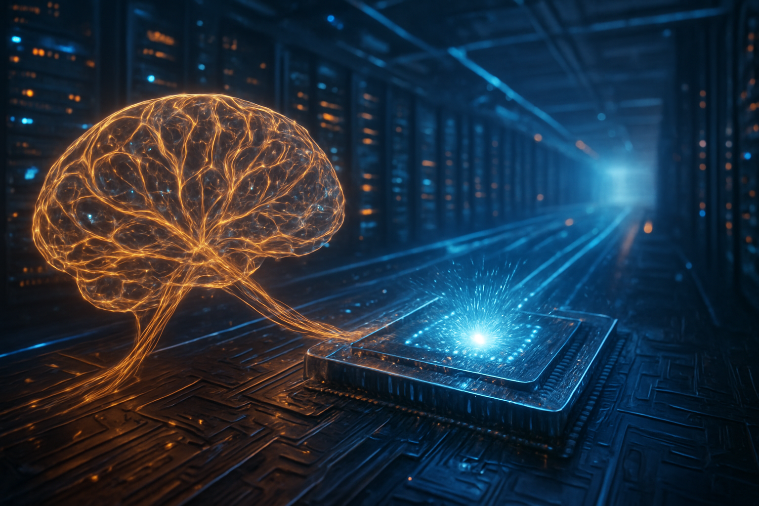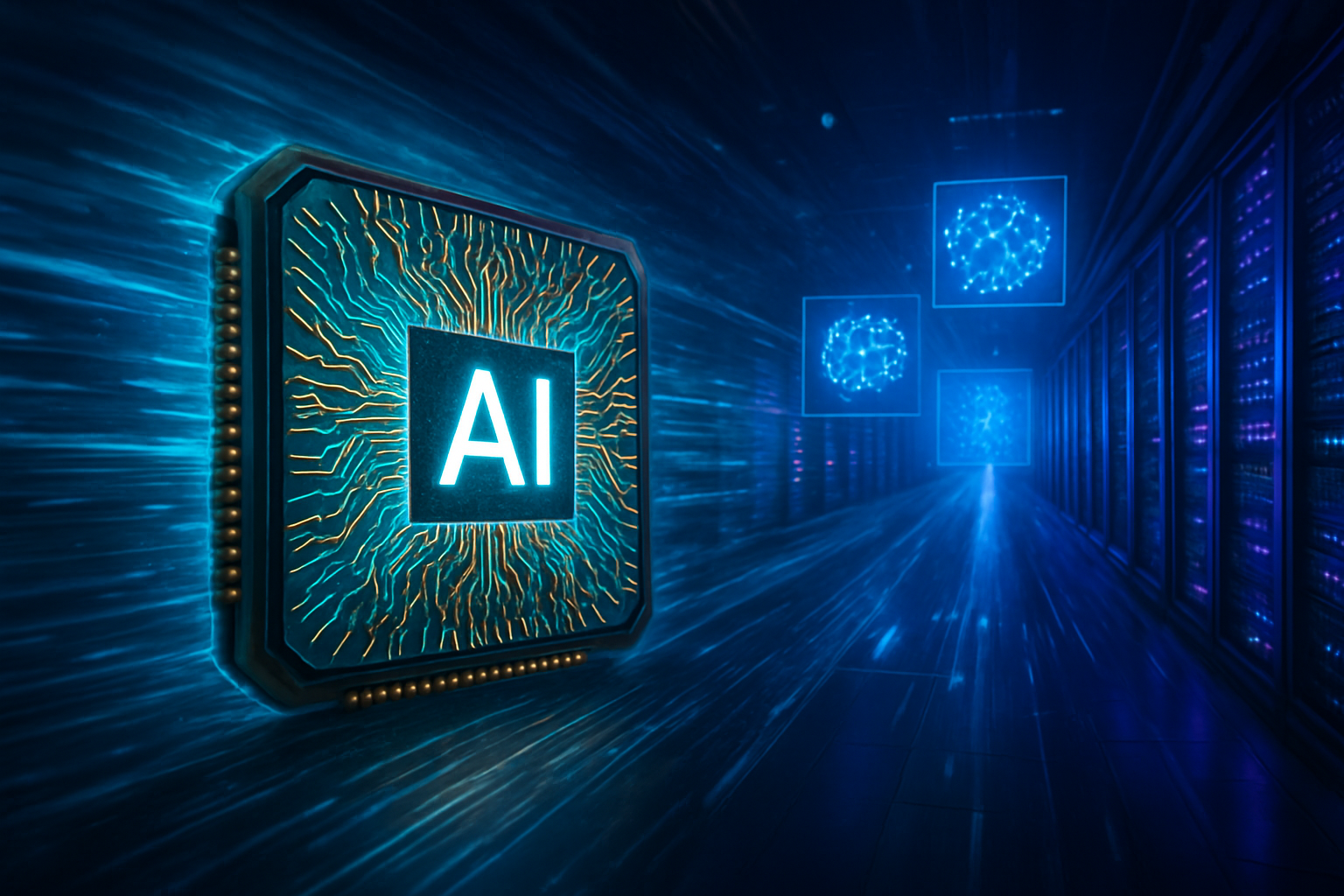
The artificial intelligence hardware landscape is undergoing a seismic shift, characterized by industry analysts as the "Great Decoupling." As of late 2025, the world’s largest cloud providers—Alphabet Inc. (NASDAQ: GOOGL), Amazon.com Inc. (NASDAQ: AMZN), and Meta Platforms Inc. (NASDAQ: META)—have reached a critical mass in their efforts to reduce reliance on NVIDIA (NASDAQ: NVDA). This movement is no longer a series of experimental projects but a full-scale industrial pivot toward custom Application-Specific Integrated Circuits (ASICs) designed to optimize performance and bypass the high premiums associated with third-party hardware.
The immediate significance of this shift is most visible in the high-volume inference market, where custom silicon now captures nearly 40% of all workloads. By deploying their own chips, these hyperscalers are effectively avoiding the "NVIDIA tax"—the 70% to 80% gross margins commanded by the market leader—while simultaneously tailoring their hardware to the specific needs of their massive software ecosystems. While NVIDIA remains the undisputed champion of frontier model training, the rise of specialized silicon for inference marks a new era of cost-efficiency and architectural sovereignty for the tech giants.
Silicon Sovereignty: The Specs Behind the Shift
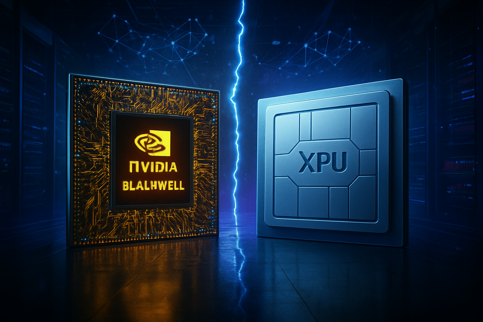
The technical vanguard of this movement is led by Google’s seventh-generation Tensor Processing Unit, codenamed TPU v7 'Ironwood.' Unveiled with staggering specifications, Ironwood claims a performance of 4.6 PetaFLOPS of dense FP8 compute per chip. This puts it in a dead heat with NVIDIA’s Blackwell B200 architecture. Beyond raw speed, Google has optimized Ironwood for massive scale, utilizing an Optical Circuit Switch (OCS) fabric that allows the company to link 9,216 chips into a single "Superpod" with nearly 2 Petabytes of shared memory. This architecture is specifically designed to handle the trillion-parameter models that define the current state of generative AI.
Not to be outdone, Amazon has scaled its Trainium3 and Inferentia lines, moving to a unified 3nm process for its latest silicon. The Trainium3 UltraServer integrates 144 chips per rack to aggregate 362 FP8 PetaFLOPS, offering a 30% to 40% price-performance advantage over general-purpose GPUs for AWS customers. Meanwhile, Meta’s MTIA v2 (Artemis) has seen broad deployment across its global data center footprint. Unlike its competitors, Meta has prioritized a massive SRAM hierarchy over expensive High Bandwidth Memory (HBM) for its specific recommendation and ranking workloads, resulting in a 44% lower Total Cost of Ownership (TCO) compared to commercial alternatives.
Industry experts note that this differs fundamentally from previous hardware cycles. In the past, general-purpose GPUs were necessary because AI algorithms were changing too rapidly for fixed-function ASICs to keep up. However, the maturation of the Transformer architecture and the standardization of data types like FP8 have allowed hyperscalers to "freeze" certain hardware requirements into silicon without the risk of immediate obsolescence.
Competitive Implications for the AI Ecosystem
The "Great Decoupling" is creating a bifurcated market that benefits the hyperscalers while forcing NVIDIA to accelerate its own innovation cycle. For Alphabet, Amazon, and Meta, the primary benefit is margin expansion. By "paying cost" for their own silicon rather than market prices, these companies can offer AI services at a price point that is difficult for smaller cloud competitors to match. This strategic advantage allows them to subsidize their AI research and development through hardware savings, creating a virtuous cycle of reinvestment.
For NVIDIA, the challenge is significant but not yet existential. The company still maintains a 90% share of the frontier model training market, where flexibility and absolute peak performance are paramount. However, as inference—the process of running a trained model for users—becomes the dominant share of AI compute spending, NVIDIA is being pushed into a "premium tier" where it must justify its costs through superior software and networking. The erosion of the "CUDA Moat," driven by the rise of open-source compilers like OpenAI’s Triton and PyTorch 2.x, has made it significantly easier for developers to port their models to Google’s TPUs or Amazon’s Trainium without a massive engineering overhead.
Startups and smaller AI labs stand to benefit from this competition as well. The availability of diversified hardware options in the cloud means that the "compute crunch" of 2023 and 2024 has largely eased. Companies can now choose hardware based on their specific needs: NVIDIA for cutting-edge research, and custom ASICs for cost-effective, large-scale deployment.
The Economic and Strategic Significance
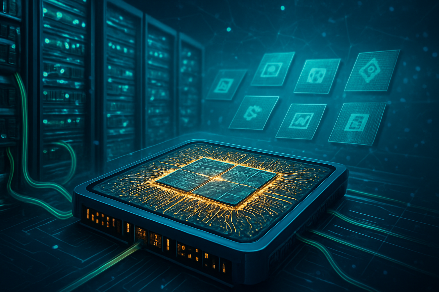
The wider significance of this shift lies in the democratization of high-performance compute at the infrastructure level. We are moving away from a monolithic hardware era toward a specialized one. This fits into the broader trend of "vertical integration," where the software, the model, and the silicon are co-designed. When a company like Meta designs a chip specifically for its recommendation algorithms, it achieves efficiencies that a general-purpose chip simply cannot match, regardless of its raw power.
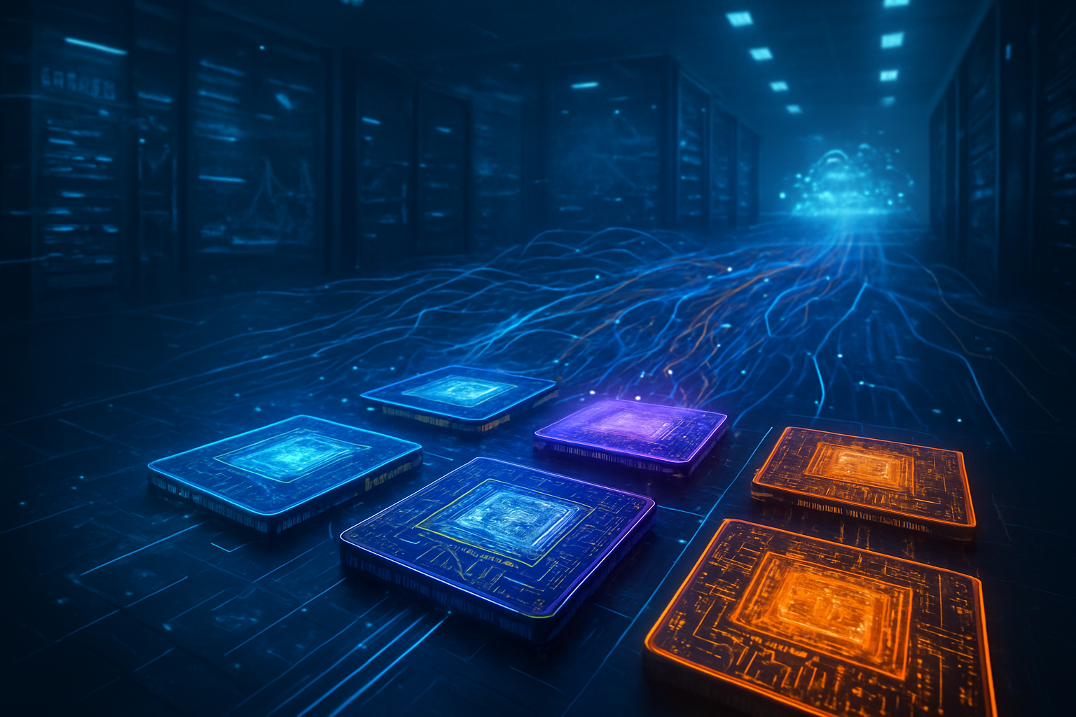
However, this transition is not without concerns. The reliance on custom silicon could lead to "vendor lock-in" at the hardware level, where a model optimized for Google’s TPU v7 may not perform as well on Amazon’s Trainium3. Furthermore, the massive capital expenditure required to design and manufacture 3nm chips means that only the wealthiest companies can participate in this decoupling. This could potentially centralize AI power even further among the "Magnificent Seven" tech giants, as the cost of entry for custom silicon is measured in billions of dollars.
Comparatively, this milestone is being likened to the transition from general-purpose CPUs to GPUs in the early 2010s. Just as the GPU unlocked the potential of deep learning, the custom ASIC is unlocking the potential of "AI at scale," making it economically viable to serve generative AI to billions of users simultaneously.
Future Horizons: Beyond the 3nm Era
Looking ahead, the next 24 to 36 months will see an even more aggressive roadmap. NVIDIA is already preparing its Rubin architecture, which is expected to debut in late 2026 with HBM4 memory and "Vera" CPUs, aiming to reclaim the performance lead. In response, hyperscalers are already in the design phase for their next-generation chips, focusing on "chiplet" architectures that allow for even more modular and scalable designs.
We can expect to see more specialized use cases on the horizon, such as "edge ASICs" designed for local inference on mobile devices and IoT hardware, further extending the reach of these custom stacks. The primary challenge remains the supply chain; as everyone moves to 3nm and 2nm processes, the competition for manufacturing capacity at foundries like TSMC will be the ultimate bottleneck. Experts predict that the next phase of the hardware wars will not just be about who has the best design, but who has the most secure access to the world’s most advanced fabrication plants.
A New Chapter in AI History
In summary, the deployment of custom silicon by hyperscalers represents a maturing of the AI industry. The transition from a single-provider market to a diversified ecosystem of custom ASICs is a clear signal that AI has moved from the research lab to the core of global infrastructure. Key takeaways include the impressive 4.6 PetaFLOPS performance of Google’s Ironwood, the significant TCO advantages of Meta’s MTIA v2, and the strategic necessity for cloud giants to escape the "NVIDIA tax."
As we move into 2026, the industry will be watching for the first large-scale frontier models trained entirely on non-NVIDIA hardware. If a company like Google or Meta can produce a GPT-5 class model using only internal silicon, it will mark the final stage of the Great Decoupling. For now, the hardware wars are heating up, and the ultimate winners will be the users who benefit from more powerful, more efficient, and more accessible artificial intelligence.
This content is intended for informational purposes only and represents analysis of current AI developments.
TokenRing AI delivers enterprise-grade solutions for multi-agent AI workflow orchestration, AI-powered development tools, and seamless remote collaboration platforms.
For more information, visit https://www.tokenring.ai/.