As of late 2025, the semiconductor industry stands at the precipice of a profound transformation, driven by an insatiable demand for computational power across Artificial Intelligence (AI), High-Performance Computing (HPC), and the rapidly evolving mobile sector. This period marks a pivotal shift beyond the conventional limits of Moore's Law, as groundbreaking advancements in chip design and novel architectures are fundamentally redefining how technology delivers intelligence and performance. These innovations are not merely incremental improvements but represent a systemic re-architecture of computing, promising to unlock unprecedented capabilities and reshape the technological landscape for decades to come.
The immediate significance of these developments cannot be overstated. From enabling the real-time processing of colossal AI models to facilitating complex scientific simulations and powering smarter, more efficient mobile devices, the next generation of semiconductors is the bedrock upon which future technological breakthroughs will be built. This foundational shift is poised to accelerate innovation across industries, fostering an era of more intelligent systems, faster data analysis, and seamlessly integrated digital experiences.
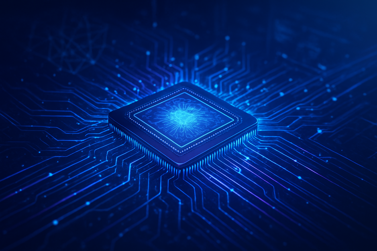
Technical Revolution: Unpacking the Next-Gen Semiconductor Landscape
The core of this revolution lies in several intertwined technical advancements that are collectively pushing the boundaries of what's possible in silicon.
The most prominent shift is towards Advanced Packaging and Heterogeneous Integration, particularly through chiplet technology. Moving away from monolithic System-on-Chip (SoC) designs, manufacturers are now integrating multiple specialized "chiplets"—each optimized for a specific function like logic, memory, or I/O—into a single package. This modular approach offers significant advantages: vastly increased performance density, improved energy efficiency through closer proximity and advanced interconnects, and highly customizable architectures tailored for specific AI, HPC, or embedded applications. Technologies like 2.5D and 3D stacking, including chip-on-wafer-on-substrate (CoWoS) and through-silicon vias (TSVs), are critical enablers, providing ultra-short, high-density connections that drastically reduce latency and power consumption. Early prototypes of monolithic 3D integration, where layers are built sequentially on the same wafer, are also demonstrating substantial gains in both performance and energy efficiency.
Concurrently, the relentless pursuit of smaller process nodes continues, albeit with increasing complexity. By late 2025, the industry is seeing the widespread adoption of 3-nanometer (nm) and 2nm manufacturing processes. Leading foundries like TSMC (NYSE: TSM) are on track with their A16 (1.6nm) nodes for production in 2026, while Intel (NASDAQ: INTC) is pushing towards its 1.8nm (Intel 18A) node. These finer geometries allow for higher transistor density, translating directly into superior performance and greater power efficiency, crucial for demanding AI and HPC workloads. Furthermore, the integration of advanced materials is playing a pivotal role. Silicon Carbide (SiC) and Gallium Nitride (GaN) are becoming standard for power components, offering higher breakdown voltages, faster switching speeds, and greater power density, which is particularly vital for the energy-intensive data centers powering AI and HPC. Research into novel 3D DRAM using oxide-semiconductors and carbon nanotube transistors also promises high-density, low-power memory solutions.
Perhaps one of the most intriguing developments is the increasing role of AI in chip design and manufacturing itself. AI-powered Electronic Design Automation (EDA) tools are automating complex tasks like schematic generation, layout optimization, and verification, drastically shortening design cycles—what once took months for a 5nm chip can now be achieved in weeks. AI also enhances manufacturing efficiency through predictive maintenance, real-time process optimization, and sophisticated defect detection, ensuring higher yields and faster time-to-market for these advanced chips. This self-improving loop, where AI designs better chips for AI, represents a significant departure from traditional, human-intensive design methodologies. The initial reactions from the AI research community and industry experts are overwhelmingly positive, with many hailing these advancements as the most significant architectural shifts since the rise of the GPU, setting the stage for an exponential leap in computational capabilities.
Industry Shake-Up: Winners, Losers, and Strategic Plays
The seismic shifts in semiconductor technology are poised to create significant ripples across the tech industry, reordering competitive landscapes and establishing new strategic advantages. Several key players stand to benefit immensely, while others may face considerable disruption if they fail to adapt.
NVIDIA (NASDAQ: NVDA), a dominant force in AI and HPC GPUs, is exceptionally well-positioned. Their continued innovation in GPU architectures, coupled with aggressive adoption of HBM and CXL technologies, ensures they remain at the forefront of AI training and inference. The shift towards heterogeneous integration and specialized accelerators complements NVIDIA's strategy of offering a full-stack solution, from hardware to software. Similarly, Intel (NASDAQ: INTC) and Advanced Micro Devices (NASDAQ: AMD) are making aggressive moves to capture market share. Intel's focus on advanced process nodes (like Intel 18A) and its strong play in CXL and CPU-GPU integration positions it as a formidable competitor, especially in data center and HPC segments. AMD, with its robust CPU and GPU offerings and increasing emphasis on chiplet designs, is also a major beneficiary, particularly in high-performance computing and enterprise AI.
The foundries, most notably Taiwan Semiconductor Manufacturing Company (TSMC) (NYSE: TSM) and Samsung Electronics (KRX: 005930), are critical enablers and direct beneficiaries. Their ability to deliver cutting-edge process nodes (3nm, 2nm, and beyond) and advanced packaging solutions (CoWoS, 3D stacking) makes them indispensable to the entire tech ecosystem. Companies that can secure capacity at these leading-edge foundries will gain a significant competitive edge. Furthermore, major cloud providers like Amazon (NASDAQ: AMZN) (AWS), Google (NASDAQ: GOOGL) (Google Cloud), and Microsoft (NASDAQ: MSFT) (Azure) are heavily investing in custom Application-Specific Integrated Circuits (ASICs) for their AI workloads. The chiplet approach and advanced packaging allow these tech giants to design highly optimized, cost-effective, and energy-efficient AI accelerators tailored precisely to their internal software stacks, potentially disrupting traditional GPU markets for specific AI tasks. This strategic move provides them greater control over their infrastructure, reduces reliance on third-party hardware, and can offer 10-100x efficiency improvements for specific AI operations compared to general-purpose GPUs.
Startups specializing in novel AI architectures, particularly those focused on neuromorphic computing or highly efficient edge AI processors, also stand to gain. The modularity of chiplets lowers the barrier to entry for designing specialized silicon, allowing smaller companies to innovate without the prohibitive costs of designing entire monolithic SoCs. However, established players with deep pockets and existing ecosystem advantages will likely consolidate many of these innovations. The competitive implications are clear: companies that can rapidly adopt and integrate these new chip design paradigms will thrive, while those clinging to older, less efficient architectures risk being left behind. The market is increasingly valuing power efficiency, customization, and integrated performance, forcing every major player to rethink their silicon strategy.
Wider Significance: Reshaping the AI and Tech Landscape
These anticipated advancements in semiconductor chip design and architecture are far more than mere technical upgrades; they represent a fundamental reshaping of the broader AI landscape and global technological trends. This era marks a critical inflection point, moving beyond the incremental gains of the past to a period of transformative change.
Firstly, these developments significantly accelerate the trajectory of Artificial General Intelligence (AGI) research and deployment. The massive increase in computational power, memory bandwidth, and energy efficiency provided by chiplets, HBM, CXL, and specialized accelerators directly addresses the bottlenecks that have hindered the training and inference of increasingly complex AI models, particularly large language models (LLMs). This enables researchers to experiment with larger, more intricate neural networks and develop AI systems capable of more sophisticated reasoning and problem-solving. The ability to run these advanced AIs closer to the data source, on edge devices, also expands the practical applications of AI into real-time scenarios where latency is critical.
The impact on data centers is profound. CXL, in particular, allows for memory disaggregation and pooling, turning memory into a composable resource that can be dynamically allocated across CPUs, GPUs, and accelerators. This eliminates costly over-provisioning, drastically improves utilization, and reduces the total cost of ownership for AI and HPC infrastructure. The enhanced power efficiency from smaller process nodes and advanced materials also helps mitigate the soaring energy consumption of modern data centers, addressing both economic and environmental concerns. However, potential concerns include the increasing complexity of designing and manufacturing these highly integrated systems, leading to higher development costs and the potential for a widening gap between companies that can afford to innovate at the cutting edge and those that cannot. This could exacerbate the concentration of AI power in the hands of a few tech giants.
Comparing these advancements to previous AI milestones, this period is arguably as significant as the advent of GPUs for parallel processing or the breakthroughs in deep learning algorithms. While past milestones focused on software or specific hardware components, the current wave involves a holistic re-architecture of the entire computing stack, from the fundamental silicon to system-level integration. The move towards specialized, heterogeneous computing is reminiscent of how the internet evolved from general-purpose servers to a highly distributed, specialized network. This signifies a departure from a one-size-fits-all approach to computing, embracing diversity and optimization for specific workloads. The implications extend beyond technology, touching on national security (semiconductor independence), economic competitiveness, and the ethical considerations of increasingly powerful AI systems.
The Road Ahead: Future Developments and Challenges
Looking to the horizon, the advancements in semiconductor technology promise an exciting array of near-term and long-term developments, while also presenting significant challenges that the industry must address.
In the near term, we can expect the continued refinement and widespread adoption of chiplet architectures and 3D stacking technologies. This will lead to increasingly dense and powerful processors for cloud AI and HPC, with more sophisticated inter-chiplet communication. The CXL ecosystem will mature rapidly, with CXL 3.0 and beyond enabling even more robust multi-host sharing and switching capabilities, truly unlocking composable memory and compute infrastructure in data centers. We will also see a proliferation of highly specialized edge AI accelerators integrated into a wider range of devices, from smart home appliances to industrial IoT sensors, making AI ubiquitous and context-aware. Experts predict that the performance-per-watt metric will become the primary battleground, as energy efficiency becomes paramount for both environmental sustainability and economic viability.
Longer term, the industry is eyeing monolithic 3D integration as a potential game-changer, where entire functional layers are built directly on top of each other at the atomic level, promising unprecedented performance and energy efficiency. Research into neuromorphic chips designed to mimic the human brain's neural networks will continue to advance, potentially leading to ultra-low-power AI systems capable of learning and adapting with significantly reduced energy footprints. Quantum computing, while still nascent, will also increasingly leverage advanced packaging and cryogenic semiconductor technologies. Potential applications on the horizon include truly personalized AI assistants that learn and adapt deeply to individual users, autonomous systems with real-time decision-making capabilities far beyond current capacities, and breakthroughs in scientific discovery driven by exascale HPC systems.
However, significant challenges remain. The cost and complexity of manufacturing at sub-2nm nodes are escalating, requiring immense capital investment and sophisticated engineering. Thermal management in densely packed 3D architectures becomes a critical hurdle, demanding innovative cooling solutions. Supply chain resilience is another major concern, as geopolitical tensions and the highly concentrated nature of advanced manufacturing pose risks. Furthermore, the industry faces a growing talent gap in chip design, advanced materials science, and packaging engineering. Experts predict that collaboration across the entire semiconductor ecosystem—from materials suppliers to EDA tool vendors, foundries, and system integrators—will be crucial to overcome these challenges and fully realize the potential of these next-generation semiconductors. What happens next will largely depend on sustained investment in R&D, international cooperation, and a concerted effort to nurture the next generation of silicon innovators.
Comprehensive Wrap-Up: A New Era of Intelligence
The anticipated advancements in semiconductor chip design, new architectures, and their profound implications mark a pivotal moment in technological history. The key takeaways are clear: the industry is moving beyond traditional scaling with heterogeneous integration and chiplets as the new paradigm, enabling unprecedented customization and performance density. Memory-centric architectures like HBM and CXL are revolutionizing data access and system efficiency, while specialized AI accelerators are driving bespoke intelligence across all sectors. Finally, AI itself is becoming an indispensable tool in the design and manufacturing of these sophisticated chips, creating a powerful feedback loop.
This development's significance in AI history is monumental. It provides the foundational hardware necessary to unlock the next generation of AI capabilities, from more powerful large language models to ubiquitous edge intelligence and scientific breakthroughs. It represents a shift from general-purpose computing to highly optimized, application-specific silicon, mirroring the increasing specialization seen in other mature industries. This is not merely an evolution but a revolution in how we design and utilize computing power.
Looking ahead, the long-term impact will be a world where AI is more pervasive, more powerful, and more energy-efficient than ever before. We can expect a continued acceleration of innovation in autonomous systems, personalized medicine, advanced materials science, and climate modeling. What to watch for in the coming weeks and months includes further announcements from leading chip manufacturers regarding their next-generation process nodes and packaging technologies, the expansion of the CXL ecosystem, and the emergence of new AI-specific hardware from both established tech giants and innovative startups. The race to build the most efficient and powerful silicon is far from over; in fact, it's just getting started.
This content is intended for informational purposes only and represents analysis of current AI developments.
TokenRing AI delivers enterprise-grade solutions for multi-agent AI workflow orchestration, AI-powered development tools, and seamless remote collaboration platforms.
For more information, visit https://www.tokenring.ai/.