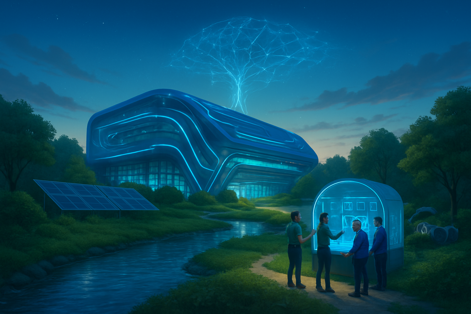
In a move that has sent shockwaves through both the aerospace and technology sectors, Elon Musk has officially announced the merger of SpaceX and xAI, creating a unified industrial and intelligence titan valued at a staggering $1.25 trillion. Announced on February 2, 2026, the deal consolidates Musk’s primary private assets—including the social media platform X, which was absorbed by xAI last year—into a singular corporate entity. This strategic union is not merely a financial consolidation; it is the cornerstone of a radical plan to move the world’s most powerful artificial intelligence infrastructure off-planet and into Earth’s orbit.
The immediate significance of this merger lies in its solution to the "AI Power Wall"—the growing realization that Earth's electrical grids and water supplies are insufficient to sustain the exponential growth of next-generation large language models. by integrating SpaceX’s launch dominance with xAI’s Grok intelligence engine, the new entity aims to bypass terrestrial limitations entirely. Industry analysts view this as the most significant corporate restructuring of the decade, signaling the transition of AI from a software service to a space-based utility.
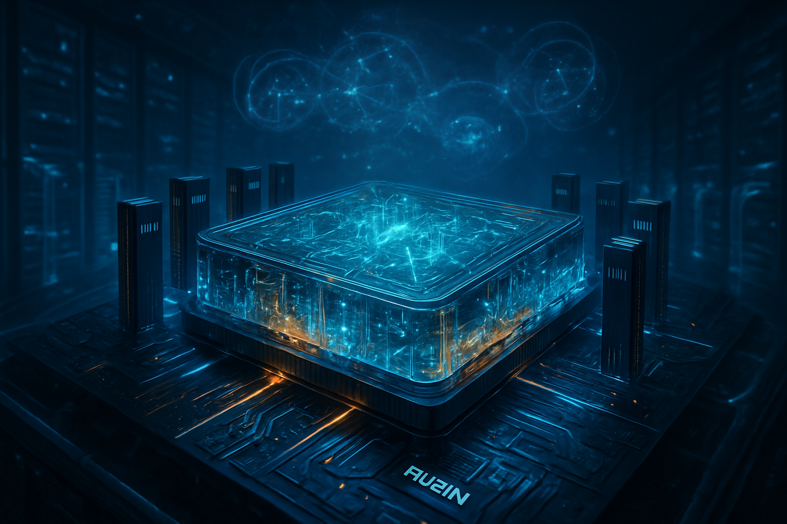
The Technical Blueprint: Engineering the First Orbital Supercomputer
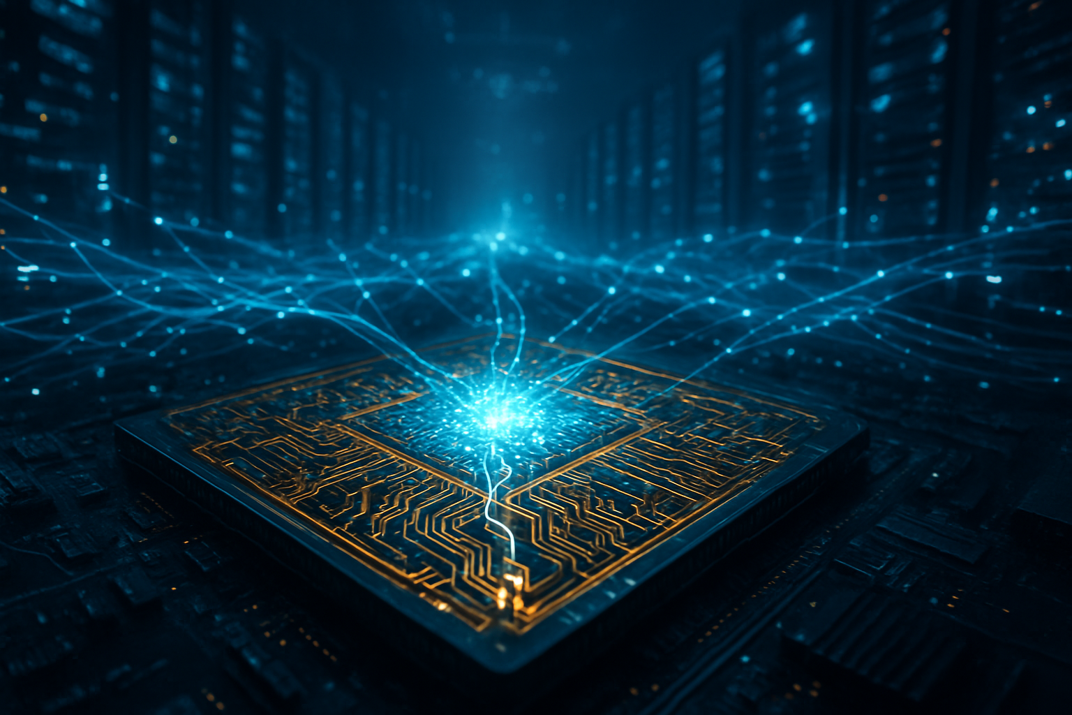
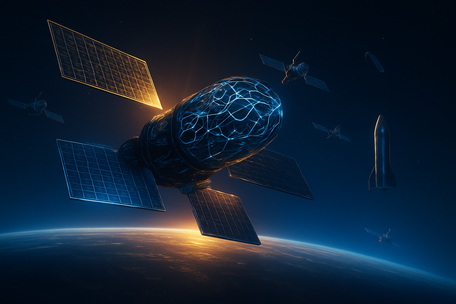
The technical core of the SpaceX-xAI merger is the "Project Celestia" initiative, which aims to deploy a constellation of up to one million specialized "compute satellites." Unlike traditional communication satellites, these nodes are designed to function as a distributed orbital supercomputer. A primary advantage is the access to nearly 100% duty-cycle solar power. By positioning these data centers in high-altitude Sun-synchronous orbits, the hardware can receive unfiltered solar energy without the interruptions of day-night cycles or atmospheric interference. Engineering data suggests that orbital solar arrays operate at up to eight times the efficiency of their terrestrial counterparts, providing a virtually infinite and sustainable power source for xAI’s compute-hungry training runs.
Perhaps even more revolutionary is the approach to thermal management. On Earth, high-performance GPUs, such as those produced by NVIDIA (NASDAQ: NVDA), require millions of gallons of water and massive HVAC systems to prevent overheating. In the vacuum of space, the new SpaceX-xAI hardware will utilize the "infinite heat sink" of the void. Through massive, high-efficiency radiator panels, waste heat is dissipated directly into space via thermal radiation, maintaining optimal operating temperatures for specialized AI silicon without consuming a single drop of water. This pivot from convection-based cooling to radiation-based cooling represents a fundamental shift in data center architecture that has remained stagnant for decades.
Connectivity between these orbital nodes will be handled by advanced inter-satellite laser links (ISLLs), creating a mesh network capable of multi-terabit data transfer speeds. This allows the orbital AI to process massive datasets—ranging from global satellite imagery to real-time communication feeds from the X platform—directly in space. The Starship launch system, now operating at a weekly cadence, provides the necessary heavy-lift capacity to deliver these multi-ton compute modules into orbit at a cost-per-kilogram that makes this infrastructure not only possible but economically superior to building on land.
A Galactic Shift in the Competitive Landscape
The merger and the subsequent orbital pivot have profound implications for the existing AI power structure. For years, Microsoft (NASDAQ: MSFT) and Alphabet (NASDAQ: GOOGL) have dominated the field through their massive terrestrial cloud footprints. However, the SpaceX-xAI merger threatens to render these land-based assets obsolete or, at the very least, ecologically and economically uncompetitive. By removing the burden of land acquisition, grid connectivity, and environmental regulations, the combined SpaceX-xAI entity can scale compute capacity at a rate that ground-bound competitors simply cannot match.
Furthermore, this move places NVIDIA (NASDAQ: NVDA) in a unique position as the primary hardware supplier for the new orbital era, though rumors persist that xAI is developing its own "space-hardened" chips to better survive cosmic radiation. Meanwhile, Amazon (NASDAQ: AMZN), through its Project Kuiper and its relationship with Blue Origin, is now under immense pressure to accelerate its own space-based compute plans. The competitive advantage of having a vertically integrated launch and AI company allows Musk to prioritize his own hardware on every Starship flight, effectively "locking out" competitors from the most efficient orbits for years to come.
Resolving the Terrestrial AI Bottleneck
The wider significance of this development cannot be overstated. We are currently witnessing the convergence of the AI revolution and the second space age. Historically, AI breakthroughs have been followed by concerns regarding the massive carbon footprint and resource strain of training models. By moving the "brain" of the internet into orbit, SpaceX and xAI are effectively decoupling technological progress from environmental degradation. This fits into the broader trend of "off-worlding" heavy industry, a concept long championed by space enthusiasts but only now made viable by the scale of the Starship program.
However, the move is not without its critics. Astronomers have already raised alarms about the potential for further light pollution and space debris from a million-satellite constellation. Moreover, the centralization of such immense computational power in the hands of a single private entity—especially one that controls its own global internet (Starlink) and social media platform (X)—raises unprecedented questions about digital sovereignty and the potential for a "monopoly on intelligence." Comparisons are being drawn to the early days of the internet, but the stakes here are much higher; we are talking about the physical infrastructure of global thought being moved beyond the reach of traditional national jurisdictions.
The Road to the Largest IPO in History
Looking ahead, the next 18 to 24 months will be a period of intense deployment. SpaceX-xAI management has already signaled that this merger is a precursor to an Initial Public Offering (IPO) targeted for the summer of 2026. Experts predict this could be the largest equity offering in history, with the goal of raising $50 billion to fund the rapid manufacturing of the compute constellation. Near-term milestones include the launch of the "Aether-1" prototype, the first 100-megawatt orbital data center module, expected to go live by the end of this year.
In the long term, we may see applications that were previously impossible due to latency or bandwidth constraints. Real-time, global-scale AI reasoning could enable everything from instant climate modeling to autonomous global logistics management handled entirely from orbit. The challenges remain significant—specifically, the need for advanced shielding to protect delicate GPU architectures from solar flares and high-energy cosmic rays. Nevertheless, the trajectory is clear: the future of AI is no longer on Earth.
A New Era of Decentralized Intelligence
The SpaceX-xAI merger marks a definitive turning point in the history of technology. By combining the means of physical transport with the means of digital intelligence, Elon Musk has created an entity that operates outside the traditional constraints of the tech industry. The transition to orbital AI data centers addresses the most pressing physical bottlenecks of the AI age—power and cooling—while simultaneously expanding the horizons of what a distributed supercomputer can achieve.
As we move toward the massive IPO later this year, the world will be watching to see if "Project Celestia" can deliver on its promise. The stakes are nothing less than the future of how humanity processes information and interacts with the stars. For now, the message from the newly merged titan is clear: to build the most advanced intelligence, we must first leave the planet.
This content is intended for informational purposes only and represents analysis of current AI developments.
TokenRing AI delivers enterprise-grade solutions for multi-agent AI workflow orchestration, AI-powered development tools, and seamless remote collaboration platforms.
For more information, visit https://www.tokenring.ai/.