Tag: Data Centers

  • The High Bandwidth Memory Wars: SK Hynix’s 400-Layer Roadmap and the Battle for AI Data Centers

    The High Bandwidth Memory Wars: SK Hynix’s 400-Layer Roadmap and the Battle for AI Data Centers

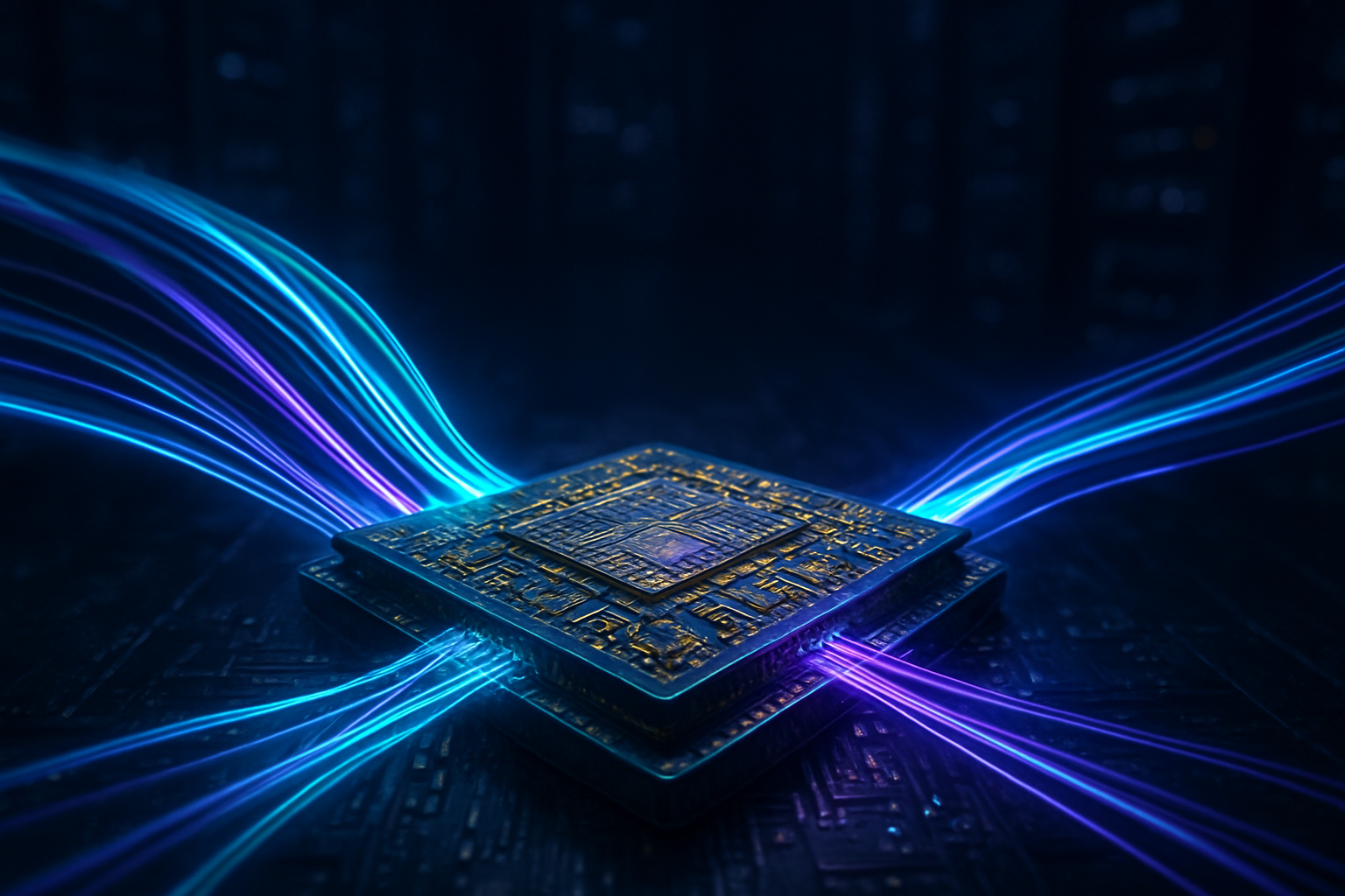
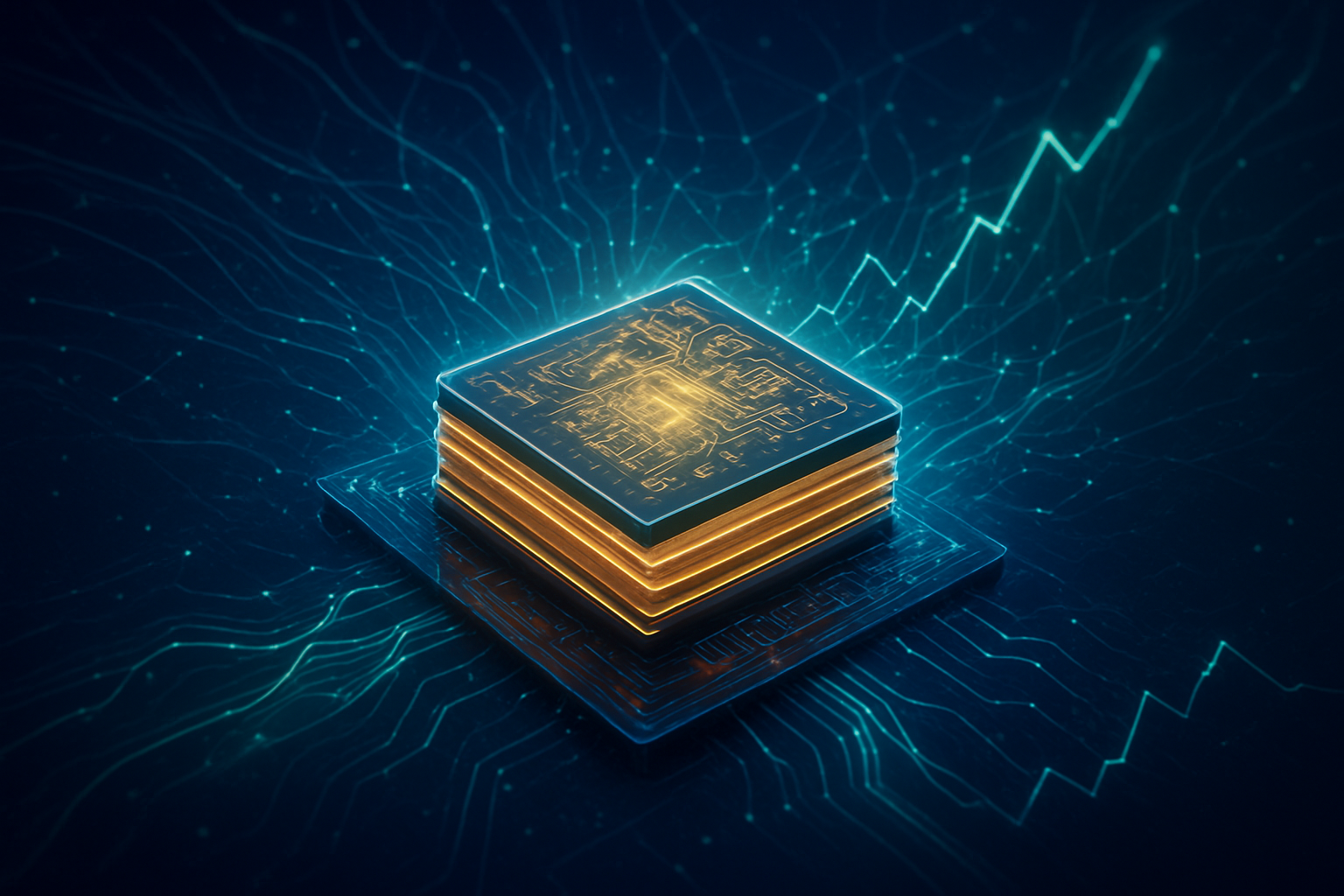
    As of December 22, 2025, the artificial intelligence revolution has shifted its primary battlefield from the logic of the GPU to the architecture of the memory chip. In a year defined by unprecedented demand for AI data centers, the "High Bandwidth Memory (HBM) Wars" have reached a fever pitch. The industry’s leaders—SK Hynix (KRX: 000660), Samsung Electronics (KRX: 005930), and Micron Technology (NASDAQ: MU)—are locked in a relentless pursuit of vertical scaling, with SK Hynix recently establishing a mass production system for HBM4 and fast-tracking its 400-layer NAND roadmap to maintain its crown as the preferred supplier for the AI elite.

    The significance of this development cannot be overstated. As AI models like GPT-5 and its successors demand exponential increases in data throughput, the "memory wall"—the bottleneck where data transfer speeds cannot keep pace with processor power—has become the single greatest threat to AI progress. By successfully transitioning to next-generation stacking technologies and securing massive supply deals for projects like OpenAI’s "Stargate," these memory titans are no longer just component manufacturers; they are the gatekeepers of the next era of computing.

    Scaling the Vertical Frontier: 400-Layer NAND and HBM4 Technicals

    The technical achievement of 2025 is the industry's shift toward the 400-layer NAND threshold and the commercialization of HBM4. SK Hynix, which began mass production of its 321-layer 4D NAND earlier this year, has officially moved to a "Hybrid Bonding" (Wafer-to-Wafer) manufacturing process to reach the 400-layer milestone. This technique involves manufacturing memory cells and peripheral circuits on separate wafers before bonding them, a radical departure from the traditional "Peripheral Under Cell" (PUC) method. This shift is essential to avoid the thermal degradation and structural instability that occur when stacking over 300 layers directly onto a single substrate.

    HBM4 represents an even more dramatic leap. Unlike its predecessor, HBM3E, which utilized a 1024-bit interface, HBM4 doubles the bus width to 2048-bit. This allows for massive bandwidth increases even at lower clock speeds, which is critical for managing the heat generated by the latest NVIDIA (NASDAQ: NVDA) Rubin-class GPUs. SK Hynix’s HBM4 production system, finalized in September 2025, utilizes advanced Mass Reflow Molded Underfill (MR-MUF) packaging, which has proven to have superior heat dissipation compared to the Thermal Compression Non-Conductive Film (TC-NCF) methods favored by some competitors.

    Initial reactions from the AI research community have been overwhelmingly positive, particularly regarding SK Hynix’s new "AIN Family" (AI-NAND). The introduction of "High-Bandwidth Flash" (HBF) effectively treats NAND storage like HBM, allowing for massive capacity in AI inference servers that were previously limited by the high cost and lower density of DRAM. Experts note that this convergence of storage and memory is the first major architectural shift in data center design in over a decade.

    The Triad Tussle: Market Positioning and Competitive Strategy

    The competitive landscape in late 2025 has seen a dramatic narrowing of the gap between the "Big Three." SK Hynix remains the market leader, commanding approximately 55–60% of the HBM market and securing over 75% of initial HBM4 orders for NVIDIA’s upcoming Rubin platform. Their strategic partnership with Taiwan Semiconductor Manufacturing Company (NYSE: TSM) for HBM4 base dies has given them a distinct advantage in integration and yield.

    However, Samsung Electronics has staged a formidable comeback. After a difficult 2024, Samsung reportedly "topped" NVIDIA’s HBM4 performance benchmarks in December 2025, leveraging its "triple-stack" technology to reach 400-layer NAND density ahead of its rivals. Samsung’s ability to act as a "one-stop shop"—providing foundry, logic, and memory services—is beginning to appeal to hyperscalers like Meta and Google who are looking to reduce their reliance on the NVIDIA-TSMC-SK Hynix triumvirate.

    Micron Technology, while currently holding the third-place position with roughly 20-25% market share, has been the most aggressive in pricing and efficiency. Micron’s HBM3E (12-layer) was a surprise success in early 2025, though the company has faced reported yield challenges with its early HBM4 samples. Despite this, Micron’s deep ties with AMD and its focus on power-efficient designs have made it a critical partner for the burgeoning "sovereign AI" projects across Europe and North America.

    The Stargate Era: Wider Significance and the Global AI Landscape

    The broader significance of the HBM wars is most visible in the "Stargate" project—a $500 billion initiative by OpenAI and Microsoft to build the world's most powerful AI supercomputer. In late 2025, both Samsung and SK Hynix signed landmark letters of intent to supply up to 900,000 DRAM wafers per month for this project by 2029. This deal essentially guarantees that the next five years of memory production are already spoken for, creating a "permanent" supply crunch for smaller players and startups.

    This concentration of resources has raised concerns about the "AI Divide." With DRAM contract prices having surged between 170% and 500% throughout 2025, the cost of training and running large-scale models is becoming prohibitive for anyone not backed by a trillion-dollar balance sheet. Furthermore, the physical limits of stacking are forcing a conversation about power consumption. AI data centers now consume nearly 40% of global memory output, and the energy required to move data from memory to processor is becoming a major environmental hurdle.

    The HBM4 transition also marks a geopolitical shift. The announcement of "Stargate Korea"—a massive data center hub in South Korea—highlights how memory-producing nations are leveraging their hardware dominance to secure a seat at the table of AI policy and development. This is no longer just about chips; it is about which nations control the infrastructure of intelligence.

    Looking Ahead: The Road to 500 Layers and HBM4E

    The roadmap for 2026 and beyond suggests that the vertical race is far from over. Industry insiders predict that the first "500-layer" NAND prototypes will appear by late 2026, likely utilizing even more exotic materials and "quad-stacking" techniques. In the HBM space, the focus will shift toward HBM4E (Extended), which is expected to push pin speeds beyond 12 Gbps, further narrowing the gap between on-chip cache and off-chip memory.

    Potential applications on the horizon include "Edge-HBM," where high-bandwidth memory is integrated into consumer devices like smartphones and laptops to run trillion-parameter models locally. However, the industry must first address the challenge of "yield maturity." As stacking becomes more complex, a single defect in one of the 400+ layers can ruin an entire wafer. Addressing these manufacturing tolerances will be the primary focus of R&D budgets in the coming 12 to 18 months.

    Summary of the Memory Revolution

    The HBM wars of 2025 have solidified the role of memory as the cornerstone of the AI era. SK Hynix’s leadership in HBM4 and its aggressive 400-layer NAND roadmap have set a high bar, but the resurgence of Samsung and the persistence of Micron ensure a competitive environment that will continue to drive rapid innovation. The key takeaways from this year are the transition to hybrid bonding, the doubling of bandwidth with HBM4, and the massive long-term supply commitments that have reshaped the global tech economy.

    As we look toward 2026, the industry is entering a phase of "scaling at all costs." The battle for memory supremacy is no longer just a corporate rivalry; it is the fundamental engine driving the AI boom. Investors and tech leaders should watch closely for the volume ramp-up of the NVIDIA Rubin platform in early 2026, as it will be the first real-world test of whether these architectural breakthroughs can deliver on their promises of a new age of artificial intelligence.


    This content is intended for informational purposes only and represents analysis of current AI developments.

    TokenRing AI delivers enterprise-grade solutions for multi-agent AI workflow orchestration, AI-powered development tools, and seamless remote collaboration platforms.
    For more information, visit https://www.tokenring.ai/.

  • Powering the Intelligence Explosion: Navitas Semiconductor’s 800V Revolution Redefines AI Data Centers and Electric Mobility

    Powering the Intelligence Explosion: Navitas Semiconductor’s 800V Revolution Redefines AI Data Centers and Electric Mobility

    As the world grapples with the insatiable power demands of the generative AI era, Navitas Semiconductor (Nasdaq: NVTS) has emerged as a pivotal architect of the infrastructure required to sustain it. By spearheading a transition to 800V high-voltage architectures, the company is effectively dismantling the "energy wall" that threatened to stall the deployment of next-generation AI clusters and the mass adoption of ultra-fast-charging electric vehicles.

    This technological pivot marks a fundamental shift in how electricity is managed at the edge of compute and mobility. As of December 2025, the industry has moved beyond traditional silicon-based power systems, which are increasingly seen as the bottleneck in the race for AI supremacy. Navitas’s integrated approach, combining Gallium Nitride (GaN) and Silicon Carbide (SiC) technologies, is now the gold standard for efficiency, enabling the 120kW+ server racks and 18-minute EV charging cycles that define the current technological landscape.

    The 12kW Breakthrough: Engineering the "AI Factory"

    The technical cornerstone of this revolution is Navitas’s dual-engine strategy, which pairs its GaNSafe™ and GeneSiC™ platforms to achieve unprecedented power density. In May 2025, Navitas unveiled its 12kW power supply unit (PSU), a device roughly the size of a laptop charger that delivers enough energy to power an entire residential block. Utilizing the IntelliWeave™ digital control platform, these units achieve over 97% efficiency, a critical metric when every fraction of a percentage point in energy loss translates into millions of dollars in cooling costs for hyperscale data centers.

    This advancement is a radical departure from the 54V systems that dominated the industry just two years ago. At 54V, delivering the thousands of amps required by modern GPUs like NVIDIA’s (Nasdaq: NVDA) Blackwell and the new Rubin Ultra series resulted in massive "I²R" heat losses and required thick, heavy copper busbars. By moving to an 800V High-Voltage Direct Current (HVDC) architecture—codenamed "Kyber" in Navitas’s latest collaboration with NVIDIA—the system can deliver the same power with significantly lower current. This reduces copper wiring requirements by 45% and eliminates multiple energy-sapping AC-to-DC conversion stages, allowing for more compute density within the same physical footprint.

    Initial reactions from the AI research community have been overwhelmingly positive, with engineers noting that the 800V shift is as much a thermal management breakthrough as it is a power one. By integrating sub-350ns short-circuit protection directly into the GaNSafe chips, Navitas has also addressed the reliability concerns that previously plagued high-voltage wide-bandgap semiconductors, making them viable for the mission-critical "always-on" nature of AI factories.

    Market Positioning: The Pivot to High-Margin Infrastructure

    Navitas’s strategic trajectory throughout 2025 has seen the company aggressively pivot away from low-margin consumer electronics toward the high-stakes sectors of AI, EV, and solar energy. This "Navitas 2.0" strategy has positioned the company as a direct challenger to legacy giants like Infineon Technologies (OTC: IFNNY) and STMicroelectronics (NYSE: STM). While STMicroelectronics continues to hold a strong grip on the Tesla (Nasdaq: TSLA) supply chain, Navitas has carved out a leadership position in the burgeoning 800V AI data center market, which is projected to reach $2.6 billion by 2030.

    The primary beneficiaries of this development are the "Magnificent Seven" tech giants and specialized AI cloud providers. For companies like Microsoft (Nasdaq: MSFT) and Alphabet (Nasdaq: GOOGL), the adoption of Navitas’s 800V technology allows them to pack more GPUs into existing data center shells, deferring billions in capital expenditure for new facility construction. Furthermore, Navitas’s recent partnership with Cyient Semiconductors to build a GaN ecosystem in India suggests a strategic move to diversify the global supply chain, providing a hedge against geopolitical tensions that have historically impacted the semiconductor industry.

    Competitive implications are stark: traditional silicon power chipmakers are finding themselves sidelined in the high-performance tier. As AI chips exceed the 1,000W-per-GPU threshold, the physical properties of silicon simply cannot handle the heat and switching speeds required. This has forced a consolidation in the industry, with companies like Wolfspeed (NYSE: WOLF) and Texas Instruments (Nasdaq: TXN) racing to scale their own 200mm SiC and GaN production lines to match Navitas's specialized "pure-play" efficiency.

    The Wider Significance: Breaking the Energy Wall

    The 800V revolution is more than just a hardware upgrade; it is a necessary evolution in the face of a global energy crisis. As AI compute demand is expected to consume up to 10% of global electricity by 2030, the efficiency gains provided by wide-bandgap materials like GaN and SiC have become a matter of environmental and economic survival. Navitas’s technology directly addresses the "Energy Wall," a point where the cost and heat of power delivery would theoretically cap the growth of AI intelligence.

    Comparisons are being drawn to the transition from vacuum tubes to transistors in the mid-20th century. Just as the transistor allowed for the miniaturization and proliferation of computers, 800V power semiconductors are allowing for the "physicalization" of AI—moving it from massive, centralized warehouses into more compact, efficient, and even mobile forms. However, this shift also raises concerns about the concentration of power (both literal and figurative) within the few companies that control the high-efficiency semiconductor supply chain.

    Sustainability advocates have noted that while the 800V shift saves energy, the sheer scale of AI expansion may still lead to a net increase in carbon emissions. Nevertheless, the ability to reduce copper usage by hundreds of kilograms per rack and improve EV range by 10% through GeneSiC traction inverters represents a significant step toward a more resource-efficient future. The 800V architecture is now the bridge between the digital intelligence of AI and the physical reality of the power grid.

    Future Horizons: From 800V to Grid-Scale Intelligence

    Looking ahead to 2026 and beyond, the industry expects Navitas to push the boundaries even further. The recent announcement of a 2300V/3300V Ultra-High Voltage (UHV) SiC portfolio suggests that the company is looking past the data center and toward the electrical grid itself. These devices could enable solid-state transformers and grid-scale energy storage systems that are smaller and more efficient than current infrastructure, potentially integrating renewable energy sources directly into AI data centers.

    In the near term, the focus remains on the "Rubin Ultra" generation of AI chips. Navitas has already unveiled 100V GaN FETs optimized for the point-of-load power boards that sit directly next to these processors. The challenge will be scaling production to meet the explosive demand while maintaining the rigorous quality standards required for automotive and hyperscale applications. Experts predict that the next frontier will be "Vertical Power Delivery," where power semiconductors are mounted directly beneath the AI chip to further reduce path resistance and maximize performance.

    A New Era of Power Electronics

    Navitas Semiconductor’s 800V revolution represents a definitive chapter in the history of AI development. By solving the physical constraints of power delivery, they have provided the "oxygen" for the AI fire to continue burning. The transition from silicon to GaN and SiC is no longer a future prospect—it is the present reality of 2025, driven by the dual engines of high-performance compute and the electrification of transport.

    The significance of this development cannot be overstated: without the efficiency gains of 800V architectures, the current trajectory of AI scaling would be economically and physically impossible. In the coming weeks and months, industry watchers should look for the first production-scale deployments of the 12kW "Kyber" racks and the expansion of GaNSafe technology into mainstream, affordable electric vehicles. Navitas has successfully positioned itself not just as a component supplier, but as a fundamental enabler of the 21st-century technological stack.


    This content is intended for informational purposes only and represents analysis of current AI developments.

    TokenRing AI delivers enterprise-grade solutions for multi-agent AI workflow orchestration, AI-powered development tools, and seamless remote collaboration platforms.
    For more information, visit https://www.tokenring.ai/.

  • Silicon Geopolitics: US Development Finance Agency Triples AI Funding to Secure Global Tech Dominance

    Silicon Geopolitics: US Development Finance Agency Triples AI Funding to Secure Global Tech Dominance

    In a decisive move to reshape the global technology landscape, the U.S. International Development Finance Corporation (DFC) has announced a massive strategic expansion into artificial intelligence (AI) infrastructure and critical mineral supply chains. As of December 2025, the agency is moving to triple its funding capacity for AI data centers and high-tech manufacturing, marking a pivot from traditional infrastructure aid to a "silicon-first" foreign policy. This expansion is designed to provide a high-standards alternative to China’s Digital Silk Road, ensuring that the next generation of AI development remains anchored in Western-aligned standards and technologies.

    The shift comes at a critical juncture as the global demand for AI compute and the minerals required to power it—such as lithium, cobalt, and rare earth elements—reaches unprecedented levels. By leveraging its expanded $200 billion contingent liability cap, authorized under the DFC Modernization and Reauthorization Act of 2025, the agency is positioning itself as the primary "de-risker" for American tech giants entering emerging markets. This strategy not only secures the physical infrastructure of the digital age but also safeguards the raw materials essential for the semiconductors and batteries that define modern industrial power.

    The Rise of the "AI Factory": Technical Expansion and Funding Tripling

    The core of the DFC’s new strategy is the "AI Horizon Fund," a multi-billion dollar initiative aimed at building "AI Factories"—large-scale data centers optimized for massive GPU clusters—across the Global South. Unlike traditional data centers, these facilities are being designed with technical specifications to support high-density compute tasks required for Large Language Model (LLM) training and real-time inference. Initial projects include a landmark partnership with Cassava Technologies to build Africa’s first sovereign AI-ready data centers, powered by specialized hardware from Nvidia (NASDAQ: NVDA).

    Technically, these projects differ from previous digital infrastructure efforts by focusing on "sovereign compute" capabilities. Rather than simply providing internet connectivity, the DFC is funding the localized hardware necessary for nations to develop their own AI applications in agriculture, healthcare, and finance. This involves deploying modular, energy-efficient data center designs that can operate in regions with unstable power grids, often paired with dedicated renewable energy microgrids or small modular reactors (SMRs). The AI research community has largely lauded the move, noting that localizing compute power reduces latency and data sovereignty concerns, though some experts warn of the immense energy requirements these "factories" will impose on developing nations.

    Industry Impact: De-Risking the Global Tech Giants

    The DFC’s expansion is a significant boon for major U.S. technology companies, providing a financial safety net for ventures that would otherwise be deemed too risky for private capital alone. Microsoft (NASDAQ: MSFT) and Alphabet Inc. (NASDAQ: GOOGL) are already coordinating with the DFC to align their multi-billion dollar investments in Mexico, Africa, and Southeast Asia with U.S. strategic interests. By providing political risk insurance and direct equity investments, the DFC allows these tech giants to compete more effectively against state-subsidized Chinese firms like Huawei and Alibaba.

    Furthermore, the focus on critical minerals is creating a more resilient supply chain for companies like Tesla (NASDAQ: TSLA) and semiconductor manufacturers. The DFC has committed over $500 million to the Lobito Corridor project, a rail link designed to transport cobalt and copper from the Democratic Republic of the Congo to Western markets, bypassing Chinese-controlled logistics hubs. This strategic positioning provides U.S. firms with a competitive advantage in securing long-term supply contracts for the materials needed for high-performance AI chips and long-range EV batteries, effectively insulating them from potential export restrictions from geopolitical rivals.

    The Digital Iron Curtain: Global Significance and Resource Security

    This aggressive expansion signals the emergence of what some analysts call a "Digital Iron Curtain," where global AI standards and infrastructure are increasingly bifurcated between U.S.-aligned and China-aligned blocs. By tripling its funding for AI and minerals, the U.S. is acknowledging that AI supremacy is inseparable from resource security. The DFC’s investment in projects like the Syrah Resources graphite mine and TechMet’s rare earth processing facilities aims to break the near-monopoly held by China in the processing of critical minerals—a bottleneck that has long threatened the stability of the Western tech sector.

    However, the DFC's pivot is not without its critics. Human rights organizations have raised concerns about the environmental and social impacts of rapid mining expansion in fragile states. Additionally, the shift toward high-tech infrastructure has led to fears that traditional development goals, such as basic sanitation and primary education, may be sidelined in favor of geopolitical maneuvering. Comparisons are being drawn to the Cold War-era "space race," but with a modern twist: the winner of the AI race will not just plant a flag, but will control the very algorithms that govern global commerce and security.

    The Road Ahead: Nuclear-Powered AI and Autonomous Mining

    Looking toward 2026 and beyond, the DFC is expected to further integrate energy production with digital infrastructure. Near-term plans include the first "Nuclear-AI Hubs," where small modular reactors will provide 24/7 carbon-free power to data centers in water-scarce regions. We are also likely to see the deployment of "Autonomous Mining Zones," where DFC-funded AI technologies are used to automate the extraction and processing of critical minerals, increasing efficiency and reducing the human cost of mining in hazardous environments.

    The primary challenge moving forward will be the "talent gap." While the DFC can fund the hardware and the mines, the software expertise required to run these AI systems remains concentrated in a few global hubs. Experts predict that the next phase of DFC strategy will involve significant investments in "Digital Human Capital," creating AI research centers and technical vocational programs in partner nations to ensure that the infrastructure being built today can be maintained and utilized by local populations tomorrow.

    A New Era of Economic Statecraft

    The DFC’s transformation into a high-tech powerhouse marks a fundamental shift in how the United States projects influence abroad. By tripling its commitment to AI data centers and critical minerals, the agency has moved beyond the role of a traditional lender to become a central player in the global technology race. This development is perhaps the most significant milestone in the history of U.S. development finance, reflecting a world where economic aid is inextricably linked to national security and technological sovereignty.

    In the coming months, observers should watch for the official confirmation of the DFC’s new leadership under Ben Black, who is expected to push for even more aggressive equity deals and private-sector partnerships. As the "AI Factories" begin to come online in 2026, the success of this strategy will be measured not just by financial returns, but by the degree to which the global South adopts a Western-aligned digital ecosystem. The battle for the future of AI is no longer just being fought in the labs of Silicon Valley; it is being won in the mines of Africa and the data centers of Southeast Asia.


    This content is intended for informational purposes only and represents analysis of current AI developments.

    TokenRing AI delivers enterprise-grade solutions for multi-agent AI workflow orchestration, AI-powered development tools, and seamless remote collaboration platforms.
    For more information, visit https://www.tokenring.ai/.

  • The Great Acceleration: US House Passes SPEED Act to Fast-Track AI Infrastructure and Outpace China

    The Great Acceleration: US House Passes SPEED Act to Fast-Track AI Infrastructure and Outpace China

    In a landmark move that signals a shift from algorithmic innovation to industrial mobilization, the U.S. House of Representatives today passed the Standardizing Permitting and Expediting Economic Development (SPEED) Act (H.R. 4776). The legislation, which passed with a bipartisan 221–196 vote on December 18, 2025, represents the most significant overhaul of federal environmental and permitting laws in over half a century. Its primary objective is to dismantle the bureaucratic hurdles currently stalling the construction of massive AI data centers and the energy infrastructure required to power them, framing the "permitting gap" as a critical vulnerability in the ongoing technological cold war with China.

    The passage of the SPEED Act comes at a time when the demand for "frontier" AI models has outstripped the physical capacity of the American power grid and existing server farms. By targeting the National Environmental Policy Act (NEPA) of 1969, the bill seeks to compress the development timeline for hyperscale data centers from several years to as little as 18 months. Proponents argue that without this acceleration, the United States risks ceding its lead in Artificial General Intelligence (AGI) to adversaries who are not bound by similar regulatory constraints.

    Redefining the Regulatory Landscape: Technical Provisions of H.R. 4776

    The SPEED Act introduces several radical changes to how the federal government reviews large-scale technology and energy projects. Most notably, it mandates strict statutory deadlines: agencies now have a maximum of two years to complete Environmental Impact Statements (EIS) and just one year for simpler Environmental Assessments (EA). These deadlines can only be extended with the explicit consent of the project applicant, effectively shifting the leverage from federal regulators to private developers. Furthermore, the bill significantly expands "categorical exclusions," allowing data centers built on brownfield sites or pre-approved industrial zones to bypass lengthy environmental reviews altogether.

    Technically, the bill redefines "Major Federal Action" to ensure that the mere receipt of federal grants or loans—common in the era of the CHIPS and Science Act—does not automatically trigger a full-scale NEPA review. Under the new rules, if federal funding accounts for less than 50% of a project's total cost, it is presumed not to be a major federal action. This provision is designed to allow tech giants to leverage public-private partnerships without being bogged down in years of paperwork. Additionally, the Act limits the scope of judicial review, shortening the window to file legal challenges from six years to a mere 150 days, a move intended to curb "litigation as a weapon" used by local opposition groups.

    The initial reaction from the AI research community has been cautiously optimistic regarding the potential for "AI moonshots." Experts at leading labs note that the ability to build 100-plus megawatt clusters quickly is the only way to test the next generation of scaling laws. However, some researchers express concern that the bill’s "purely procedural" redefinition of NEPA might lead to overlooked risks in water usage and local grid stability, which are becoming increasingly critical as liquid cooling and high-density compute become the industry standard.

    Big Tech’s Industrial Pivot: Winners and Strategic Shifts

    The passage of the SPEED Act is a major victory for the "Hyperscale Four"—Microsoft (NASDAQ: MSFT), Alphabet Inc. (NASDAQ: GOOGL), Amazon.com, Inc. (NASDAQ: AMZN), and Meta Platforms, Inc. (NASDAQ: META). These companies have collectively committed hundreds of billions of dollars to AI infrastructure but have faced increasing delays in securing the 24/7 "dispatchable" power needed for their GPU clusters. Microsoft and Amazon, in particular, have been vocal proponents of the bill, arguing that the 1969 regulatory framework is fundamentally incompatible with the 12-to-18-month innovation cycles of generative AI.

    For NVIDIA Corporation (NASDAQ: NVDA), the SPEED Act serves as a powerful demand catalyst. As the primary provider of the H200 and Blackwell architectures, NVIDIA's growth is directly tied to how quickly its customers can build the physical shells to house its chips. By easing the permits for high-voltage transmission lines and substations, the bill ensures that the "NVIDIA-powered" data center boom can continue unabated. Smaller AI startups and labs like OpenAI and Anthropic also stand to benefit, as they rely on the infrastructure built by these tech giants to train their most advanced models.

    The competitive landscape is expected to shift toward companies that can master "industrial AI"—the intersection of hardware, energy, and real estate. With the SPEED Act reducing the "permitting risk," we may see tech giants move even more aggressively into direct energy production, including small modular reactors (SMRs) and natural gas plants. This creates a strategic advantage for firms with deep pockets who can now navigate a streamlined federal process to secure their own private power grids, potentially leaving smaller competitors who rely on the public grid at a disadvantage.

    The National Security Imperative and Environmental Friction

    The broader significance of the SPEED Act lies in its framing of AI infrastructure as a national security asset. Lawmakers frequently cited the "permitting gap" between the U.S. and China during floor debates, noting that China can approve and construct massive industrial facilities in a fraction of the time required in the West. By treating data centers as "critical infrastructure" akin to military bases or interstate highways, the U.S. government is effectively placing AI development on a wartime footing. This fits into a larger trend of "techno-nationalism," where economic and regulatory policy is explicitly designed to maintain a lead in dual-use technologies.

    However, this acceleration has sparked intense pushback from environmental organizations and frontline communities. Groups like the Sierra Club and Earthjustice have criticized the bill for "gutting" bedrock environmental protections. They argue that by limiting the scope of reviews to "proximately caused" effects, the bill ignores the cumulative climate impact of massive energy consumption. There is also a growing concern that the bill's technology-neutral stance will be used to fast-track natural gas pipelines to power data centers, potentially undermining the U.S.'s long-term carbon neutrality goals.

    Comparatively, the SPEED Act is being viewed as the "Manhattan Project" moment for AI infrastructure. Just as the 1940s required a radical reimagining of the relationship between science, industry, and the state, the 2020s are demanding a similar collapse of the barriers between digital innovation and physical construction. The risk, critics say, is that in the rush to beat China to AGI, the U.S. may be sacrificing the very environmental and community standards that define its democratic model.

    The Road Ahead: Implementation and the Senate Battle

    In the near term, the focus shifts to the U.S. Senate, where the SPEED Act faces a more uncertain path. While there is strong bipartisan support for "beating China," some Democratic senators have expressed reservations about the bill's impact on clean energy versus fossil fuels. If passed into law, the immediate impact will likely be a surge in permit applications for "mega-clusters"—data centers exceeding 500 MW—that were previously deemed too legally risky to pursue.

    Looking further ahead, we can expect the emergence of "AI Special Economic Zones," where the SPEED Act’s provisions are combined with state-level incentives to create massive hubs of compute and energy. Challenges remain, however, particularly regarding the physical supply chain for transformers and high-voltage cabling, which the bill does not directly address. Experts predict that while the SPEED Act solves the procedural problem, the physical constraints of the power grid will remain the final frontier for AI scaling.

    The next few months will also likely see a flurry of litigation as environmental groups test the new 150-day filing window. How the courts interpret the "purely procedural" nature of the new NEPA rules will determine whether the SPEED Act truly delivers the "Great Acceleration" its sponsors promise, or if it simply moves the gridlock from the agency office to the courtroom.

    A New Era for American Innovation

    The passage of the SPEED Act marks a definitive end to the era of "software only" AI development. It is an admission that the future of intelligence is inextricably linked to the physical world—to concrete, copper, and kilovolts. By prioritizing speed and national security over traditional environmental review processes, the U.S. House has signaled that the race for AGI is now the nation's top industrial priority.

    Key takeaways from today's vote include the establishment of hard deadlines for federal reviews, the narrowing of judicial challenges, and a clear legislative mandate to treat data centers as vital to national security. In the history of AI, this may be remembered as the moment when the "bits" finally forced a restructuring of the "atoms."

    In the coming weeks, industry observers should watch for the Senate's response and any potential executive actions from the White House to further streamline the "AI Action Plan." As the U.S. and China continue their sprint toward the technological horizon, the SPEED Act serves as a reminder that in the 21st century, the fastest code in the world is only as good as the power grid that runs it.


    This content is intended for informational purposes only and represents analysis of current AI developments.

    TokenRing AI delivers enterprise-grade solutions for multi-agent AI workflow orchestration, AI-powered development tools, and seamless remote collaboration platforms.
    For more information, visit https://www.tokenring.ai/.

  • The Fusion Frontier: Trump Media’s $6 Billion Pivot to Power the AI Revolution

    The Fusion Frontier: Trump Media’s $6 Billion Pivot to Power the AI Revolution

    In a move that has sent shockwaves through both the energy and technology sectors, Trump Media & Technology Group (NASDAQ:DJT) has announced a definitive merger agreement with TAE Technologies, a pioneer in the field of nuclear fusion. The $6 billion all-stock transaction, announced today, December 18, 2025, marks a radical strategic shift for the parent company of Truth Social. By acquiring one of the world's most advanced fusion energy firms, TMTG is pivoting from social media toward becoming a primary infrastructure provider for the next generation of artificial intelligence.

    The merger is designed to solve the single greatest bottleneck facing the AI industry: the astronomical power demands of massive data centers. As large language models and generative AI systems continue to scale, the traditional power grid has struggled to keep pace. This deal aims to create an "uncancellable" energy-and-tech stack, positioning the combined entity as a gatekeeper for the carbon-free, high-density power required to sustain American AI supremacy.

    The Technical Edge: Hydrogen-Boron Fusion and the 'Norm' Reactor

    At the heart of this merger is TAE Technologies’ unique approach to nuclear fusion, which deviates significantly from the massive "tokamak" reactors pursued by international projects like ITER. TAE utilizes an advanced beam-driven Field-Reversed Configuration (FRC), a method that creates a compact "smoke ring" of plasma that generates its own magnetic field for confinement. This plasma is then stabilized and heated using high-energy neutral particle beams. Unlike traditional designs, the FRC approach allows for a much smaller, more modular reactor that can be sited closer to industrial hubs and AI data centers.

    A key technical differentiator is TAE’s focus on hydrogen-boron (p-B11) fuel rather than the more common deuterium-tritium mix. This reaction is "aneutronic," meaning it releases energy primarily in the form of charged particles rather than high-energy neutrons. This eliminates the need for massive radiation shielding and avoids the production of long-lived radioactive waste, a breakthrough that simplifies the regulatory and safety requirements for deployment. In 2025, TAE disclosed its "Norm" prototype, a streamlined reactor that reduced complexity by 50% by relying solely on neutral beam injection for stability.

    The merger roadmap centers on the "Copernicus" and "Da Vinci" reactor generations. Copernicus, currently under construction, is designed to demonstrate net energy gain by the late 2020s. The subsequent Da Vinci reactor is the planned commercial prototype, intended to reach the 3-billion-degree Celsius threshold required for efficient hydrogen-boron fusion. Initial reactions from the research community have been cautiously optimistic, with experts noting that while the physics of p-B11 is more challenging than other fuels, the engineering advantages of an aneutronic system are unparalleled for commercial scalability.

    Disrupting the AI Energy Nexus: A New Power Player

    This merger places TMTG in direct competition with Big Tech’s own energy initiatives. Companies like Microsoft (NASDAQ:MSFT), which has a power purchase agreement with fusion startup Helion, and Alphabet (NASDAQ:GOOGL), which has invested in various fusion ventures, are now facing a competitor that is vertically integrating energy production with digital infrastructure. By securing a proprietary power source, TMTG aims to offer AI developers "sovereign" data centers that are immune to grid instability or fluctuating energy prices.

    The competitive implications are significant for major AI labs. If the TMTG-TAE entity can successfully deliver 50 MWe utility-scale fusion plants by 2026 as planned, they could provide a dedicated, carbon-free power source that bypasses the years-long waiting lists for grid connections that currently plague the industry. This "energy-first" strategy could allow TMTG to attract AI startups that are currently struggling to find the compute capacity and power necessary to train the next generation of models.

    Market analysts suggest that this move could disrupt the existing cloud service provider model. While Amazon (NASDAQ:AMZN) and Google have focused on purchasing renewable energy credits and investing in small modular fission reactors (SMRs), the promise of fusion offers a vastly higher energy density. If TAE’s technology matures, the combined company could potentially provide the cheapest and most reliable power on the planet, creating a massive strategic advantage in the "AI arms race."

    National Security and the Global Energy Dominance Agenda

    The merger is deeply intertwined with the broader geopolitical landscape of 2025. Following the "Unleashing American Energy" executive orders signed earlier this year, AI data centers have been designated as critical defense facilities. This policy shift allows the government to fast-track the licensing of advanced reactors, effectively clearing the bureaucratic hurdles that have historically slowed nuclear innovation. Devin Nunes, who will serve as Co-CEO of the new entity alongside Dr. Michl Binderbauer, framed the deal as a cornerstone of American national security.

    This development fits into a larger trend of "techno-nationalism," where energy independence and AI capability are viewed as two sides of the same coin. By integrating fusion power with TMTG’s digital assets, the company is attempting to build a resilient infrastructure that is independent of international supply chains or domestic regulatory shifts. This has raised concerns among some environmental and policy groups regarding the speed of deregulation, but the administration has maintained that "energy dominance" is the only way to ensure the U.S. remains the leader in AI.

    Comparatively, this milestone is being viewed as the "Manhattan Project" of the 21st century. While previous AI breakthroughs were focused on software and algorithms, the TMTG-TAE merger acknowledges that the future of AI is a hardware and energy problem. The move signals a transition from the era of "Big Software" to the era of "Big Infrastructure," where the companies that control the electrons will ultimately control the intelligence they power.

    The Road to 2031: Challenges and Future Milestones

    Looking ahead, the near-term focus will be the completion of the Copernicus reactor and the commencement of construction on the first 50 MWe pilot plant in 2026. The technical challenge remains immense: maintaining stable plasma at the extreme temperatures required for hydrogen-boron fusion is a feat of engineering that has never been achieved at a commercial scale. Critics point out that the "Da Vinci" reactor's goal of providing power between 2027 and 2031 is highly ambitious, given the historical delays in fusion research.

    However, the infusion of capital and political will from the TMTG merger provides TAE with a unique platform. The roadmap includes scaling from 50 MWe pilots to massive 500 MWe plants designed to sit at the heart of "AI Megacities." If successful, these plants could not only power data centers but also provide surplus energy to the local grid, potentially lowering energy costs for millions of Americans. The next few years will be critical as the company attempts to move from experimental physics to industrial-scale energy production.

    A New Chapter in AI History

    The merger of Trump Media & Technology Group and TAE Technologies represents one of the most audacious bets in the history of the tech industry. By valuing the deal at $6 billion and committing hundreds of millions in immediate capital, TMTG is betting that the future of the internet is not just social, but physical. It is an acknowledgment that the "AI revolution" is fundamentally limited by the laws of thermodynamics, and that the only way forward is to master the energy of the stars.

    As we move into 2026, the industry will be watching closely to see if the TMTG-TAE entity can meet its aggressive construction timelines. The success or failure of this venture will likely determine the trajectory of the AI-energy nexus for decades to come. Whether this merger results in a new era of unlimited clean energy or serves as a cautionary tale of technical overreach, it has undeniably changed the conversation about what it takes to power the future of intelligence.


    This content is intended for informational purposes only and represents analysis of current AI developments.

    TokenRing AI delivers enterprise-grade solutions for multi-agent AI workflow orchestration, AI-powered development tools, and seamless remote collaboration platforms.
    For more information, visit https://www.tokenring.ai/.

  • The Trillion-Dollar Gamble: Wall Street Braces for the AI Infrastructure “Financing Bubble”

    The Trillion-Dollar Gamble: Wall Street Braces for the AI Infrastructure “Financing Bubble”

    The artificial intelligence revolution has reached a precarious crossroads where the digital world meets the physical limits of the global economy. The "Big Four" hyperscalers—Microsoft Corp. (NASDAQ: MSFT), Alphabet Inc. (NASDAQ: GOOGL), Amazon.com Inc. (NASDAQ: AMZN), and Meta Platforms Inc. (NASDAQ: META)—have collectively pushed their annual capital expenditure (CAPEX) toward a staggering $400 billion. This unprecedented spending spree, aimed at erecting gigawatt-scale data centers and securing massive stockpiles of high-end chips, has ignited a fierce debate on Wall Street. While proponents argue this is the necessary foundation for a new industrial era, a growing chorus of analysts warns of a "financing bubble" fueled by circular revenue models and over-leveraged infrastructure debt.

    The immediate significance of this development lies in the shifting nature of tech investment. We are no longer in the era of "lean software" startups; we have entered the age of "heavy silicon" and "industrial AI." The sheer scale of the required capital has forced tech giants to seek unconventional financing, bringing private equity titans like Blackstone Inc. (NYSE: BX) and Brookfield Asset Management (NYSE: BAM) into the fold as the "new utilities" of the digital age. However, as 2025 draws to a close, the first cracks in this massive financial edifice are beginning to appear, with high-profile project cancellations and power grid failures signaling that the "Great Execution" phase of AI may be more difficult—and more expensive—than anyone anticipated.

    The Architecture of the AI Arms Race

    The technical and financial architecture supporting the AI build-out in 2025 differs radically from previous cloud expansions. Unlike the general-purpose data centers of the 2010s, today’s "AI Gigafactories" are purpose-built for massive-scale training and inference, requiring specialized power cooling and liquid-cooled racks to support clusters of hundreds of thousands of GPUs. To fund these behemoths, a new tier of "neocloud" providers like CoreWeave and Lambda Labs has pioneered the use of GPU-backed debt. In this model, the latest H100 and B200 chips from NVIDIA Corp. (NASDAQ: NVDA) serve as collateral for multi-billion dollar loans. As of late 2025, over $20 billion in such debt has been issued, often structured through Special Purpose Vehicles (SPVs) that allow companies to keep massive infrastructure liabilities off their primary corporate balance sheets.

    This shift toward asset-backed financing has been met with mixed reactions from the AI research community and industry experts. While researchers celebrate the unprecedented compute power now available for "Agentic AI" and frontier models, financial experts are drawing uncomfortable parallels to the "vendor-financing" bubble of the 1990s fiber-optic boom. In that era, equipment manufacturers financed their own customers to inflate sales figures—a dynamic some see mirrored today as hyperscalers invest in AI startups like OpenAI and Anthropic, who then use those very funds to purchase cloud credits from their investors. This "circularity" has raised concerns that the current revenue growth in the AI sector may be an accounting mirage rather than a reflection of genuine market demand.

    The technical specifications of these projects are also hitting a physical wall. The North American Electric Reliability Corporation (NERC) recently issued a winter reliability alert for late 2025, noting that AI-driven demand has added 20 gigawatts to the U.S. grid in just one year. This has led to the emergence of "stranded capital"—data centers that are fully built and equipped with billions of dollars in silicon but cannot be powered due to transformer shortages or grid bottlenecks. A high-profile example occurred on December 17, 2025, when Blue Owl Capital reportedly withdrew support for a $10 billion Oracle Corp. (NYSE: ORCL) data center project in Michigan, citing concerns over the project's long-term viability and the parent company's mounting debt.

    Strategic Shifts and the New Infrastructure Titans

    The implications for the tech industry are profound, creating a widening chasm between the "haves" and "have-nots" of the AI era. Microsoft and Amazon, with their deep pockets and "behind-the-meter" nuclear power investments, stand to benefit from their ability to weather the financing storm. Microsoft, in particular, reported a record $34.9 billion in CAPEX in a single quarter this year, signaling its intent to dominate the infrastructure layer at any cost. Meanwhile, NVIDIA continues to hold a strategic advantage as the sole provider of the "collateral" powering the debt market, though its stock has recently faced pressure as analysts move to a "Hold" rating, citing a deteriorating risk-reward profile as the market saturates.

    However, the competitive landscape is shifting for specialized AI labs and startups. The recent 62% plunge in CoreWeave’s valuation from its 2025 peak has sent shockwaves through the "neocloud" sector. These companies, which positioned themselves as agile alternatives to the hyperscalers, are now struggling with the high interest payments on their GPU-backed loans and execution failures at massive construction sites. For major AI labs, the rising cost of compute is forcing a strategic pivot toward "inference efficiency" rather than raw training power, as the cost of capital makes the "brute force" approach to AI development increasingly unsustainable for all but the largest players.

    Market positioning is also being redefined by the "Great Rotation" on Wall Street. Institutional investors are beginning to pull back from capital-intensive hardware plays, leading to significant sell-offs in companies like Arm Holdings (NASDAQ: ARM) and Broadcom Inc. (NASDAQ: AVGO) in December 2025. These firms, once the darlings of the AI boom, are now under intense scrutiny for their gross margin contraction and the perceived "lackluster" execution of their AI-related product lines. The strategic advantage has shifted from those who can build the most to those who can prove the highest return on invested capital (ROIC).

    The Widening ROI Gap and Grid Realities

    This financing crunch fits into a broader historical pattern of technological over-exuberance followed by a painful "reality check." Much like the rail boom of the 19th century or the internet build-out of the 1990s, the current AI infrastructure phase is characterized by a "build it and they will come" mentality. The wider significance of this moment is the realization that while AI software may scale at the speed of light, AI hardware and power scale at the speed of copper, concrete, and regulatory permits. The "ROI Gap"—the distance between the $600 billion spent on infrastructure and the actual revenue generated by AI applications—has become the defining metric of 2025.

    Potential concerns regarding the energy grid have also moved from theoretical to existential. In Northern Virginia's "Data Center Alley," a near-blackout in early December 2025 exposed the fragility of the current system, where 1.5 gigawatts of load nearly crashed the regional transmission network. This has prompted legislative responses, such as a new Texas law requiring remote-controlled shutoff switches for large data centers, allowing grid operators to forcibly cut power to AI facilities during peak residential demand. These developments suggest that the "AI revolution" is no longer just a Silicon Valley story, but a national security and infrastructure challenge.

    Comparisons to previous AI milestones, such as the release of GPT-4, show a shift in focus from "capability" to "sustainability." While the breakthroughs of 2023 and 2024 proved that AI could perform human-like tasks, the challenges of late 2025 are proving that doing so at scale is a logistical and financial nightmare. The "financing bubble" fears are not necessarily a prediction of AI's failure, but rather a warning that the current pace of capital deployment is disconnected from the pace of enterprise adoption. According to a recent MIT study, while 95% of organizations have yet to see a return on GenAI, a small elite group of "Agentic AI Early Adopters" is seeing an 88% positive ROI, suggesting a bifurcated future for the industry.

    The Horizon: Consolidation and Efficiency

    Looking ahead, the next 12 to 24 months will likely be defined by a shift toward "Agentic SaaS" and the integration of small modular reactors (SMRs) to solve the power crisis. Experts predict that the "ROI Gap" will either begin to close as autonomous AI agents take over complex enterprise workflows, or the industry will face a "Great Execution" crisis by 2027. We expect to see a wave of consolidation in the "neocloud" space, as over-leveraged startups are absorbed by hyperscalers or private equity firms with the patience to wait for long-term returns.

    The challenge of "brittle workflows" remains the primary hurdle for near-term developments. Gartner predicts that up to 40% of Agentic AI projects will be canceled by 2027 because they fail to provide clear business value or prove too expensive to maintain. To address this, the industry is moving toward more efficient, domain-specific models that require less compute power. The long-term application of AI in fields like drug discovery and material science remains promising, but the path to those use cases is being rerouted through a much more disciplined financial landscape.

    A New Era of Financial Discipline

    In summary, the AI financing landscape of late 2025 is a study in extremes. On one hand, we see the largest capital deployment in human history, backed by the world's most powerful corporations and private equity funds. On the other, we see mounting evidence of a "financing bubble" characterized by circular revenue, over-leveraged debt, and physical infrastructure bottlenecks. The collapse of the Oracle-Blue Owl deal and the volatility in GPU-backed lending are clear signals that the era of "easy money" for AI is over.

    This development will likely be remembered as the moment when the AI industry grew up—the transition from a speculative land grab to a disciplined industrial sector. The long-term impact will be a more resilient, if slower-growing, AI ecosystem that prioritizes ROI and energy sustainability over raw compute scale. In the coming weeks and months, investors should watch for further "Great Rotation" movements in the markets and the quarterly earnings of the Big Four for any signs of a CAPEX pullback. The trillion-dollar gamble is far from over, but the stakes have never been higher.


    This content is intended for informational purposes only and represents analysis of current AI developments.

    TokenRing AI delivers enterprise-grade solutions for multi-agent AI workflow orchestration, AI-powered development tools, and seamless remote collaboration platforms.
    For more information, visit https://www.tokenring.ai/.

  • The 1.6T Breakthrough: How MACOM’s Analog Innovations are Powering the 100,000-GPU AI Era

    The 1.6T Breakthrough: How MACOM’s Analog Innovations are Powering the 100,000-GPU AI Era

    As of December 18, 2025, the global race for artificial intelligence supremacy has moved beyond the chip itself and into the very fabric that connects them. With Tier-1 AI labs now deploying "Gigawatt-scale" AI factories featuring upwards of 100,000 GPUs, the industry has hit a critical bottleneck: the "networking wall." To shatter this barrier, MACOM Technology Solutions (NASDAQ: MTSI) has emerged as a linchpin of the modern data center, providing the high-performance analog and mixed-signal semiconductors essential for the transition to 800G and 1.6 Terabit (1.6T) data throughput.

    The immediate significance of MACOM’s recent advancements cannot be overstated. In a year defined by the massive ramp-up of the NVIDIA (NASDAQ: NVDA) Blackwell architecture and the emergence of 200,000-GPU clusters like xAI’s Colossus, the demand for "east-west" traffic—the communication between GPUs—has reached a staggering 80 Petabits per second in some facilities. MACOM’s role in enabling 200G-per-lane connectivity and its pioneering "DSP-free" optical architectures have allowed hyperscalers to scale these clusters while slashing power consumption and latency, two factors that previously threatened to stall the progress of frontier AI models.

    The Technical Frontier: 200G Lanes and the Death of the DSP

    At the heart of MACOM’s 2025 success is the shift to 200G-per-lane technology. While 400G and early 800G networks relied on 100G lanes, the 1.6T era requires doubling that density. MACOM’s recently launched chipset portfolio for 1.6T connectivity includes Transimpedance Amplifiers (TIAs) and laser drivers capable of 212 Gbps per lane. This technical leap is facilitated by MACOM’s proprietary Indium Phosphide (InP) process, which allows for the high-sensitivity photodetectors and high-power Continuous Wave (CW) lasers necessary to maintain signal integrity at these extreme frequencies.

    One of the most disruptive technologies in MACOM’s arsenal is its PURE DRIVE™ Linear Pluggable Optics (LPO) ecosystem. Traditionally, optical modules use a Digital Signal Processor (DSP) to "clean up" the signal, but this adds significant power draw and roughly 200 nanoseconds of latency. In the world of synchronous AI training, where thousands of GPUs must wait for the slowest signal to arrive, 200 nanoseconds is an eternity. MACOM’s LPO solutions remove the DSP entirely, relying on high-performance analog components to maintain signal quality. This reduces module power consumption by up to 50% and slashes latency to under 5 nanoseconds, a feat that has drawn widespread praise from the AI research community for its ability to maximize "GPU utilization" rates.

    Furthermore, MACOM has addressed the physical constraints of the data center with its Active Copper Cable (ACC) solutions. As AI racks become more densely packed, the heat generated by traditional optics becomes unmanageable. MACOM’s linear equalizers allow copper cables to reach distances of up to 2.5 meters at 226 Gbps speeds. This allows for "in-rack" 1.6T connections to remain on copper, which is not only cheaper but also significantly more energy-efficient than optical alternatives, providing a critical "thermal relief valve" for high-density GPU clusters.

    Market Dynamics: The Beneficiaries of the Analog Renaissance

    The strategic positioning of MACOM (NASDAQ: MTSI) has made it a primary beneficiary of the massive CAPEX spending by hyperscalers like Meta (NASDAQ: META), Microsoft (NASDAQ: MSFT), and Google (NASDAQ: GOOGL). As these giants transition their backbones from 400G to 800G and 1.6T, they are increasingly looking for ways to bypass the high costs and power requirements of traditional retimed (DSP-based) modules. MACOM’s architecture-agnostic approach—supporting both retimed and linear configurations—allows it to capture market share regardless of which specific networking standard a hyperscaler adopts.

    In the competitive landscape, MACOM is carving out a unique niche against larger rivals like Broadcom (NASDAQ: AVGO) and Marvell Technology (NASDAQ: MRVL). While Broadcom dominates the switch ASIC market with its Tomahawk 6 series, MACOM provides the essential "front-end" analog components that interface with those switches. The partnership between MACOM’s analog expertise and the latest 102.4 Tbps switch chips has created a formidable ecosystem that is difficult for startups to penetrate. For AI labs, the strategic advantage of using MACOM-powered LPO modules lies in the "Total Cost of Ownership" (TCO); by reducing power by several watts per port across a 100,000-port cluster, a data center operator can save millions in annual electricity and cooling costs.

    Wider Significance: Enabling the Gigawatt-Scale AI Factory

    The rise of MACOM’s technology fits into a broader trend of "Scale-Across" architectures. In 2025, a single data center building often cannot support the 300MW to 500MW required for a 200,000-GPU cluster. This has led to the creation of virtual clusters spread across multiple buildings within a campus. MACOM’s high-performance optics are the "connective tissue" that enables these buildings to communicate with the ultra-low latency required to function as a single unit. Without the signal integrity provided by high-performance analog semiconductors, the latency introduced by distance would cause the entire AI training process to desynchronize.

    However, the rapid scaling of these facilities has also raised concerns. The environmental impact of "Gigawatt-scale" sites is under intense scrutiny. MACOM’s focus on power efficiency via DSP-free optics is not just a technical preference but a necessity for the industry’s survival in a world of limited power grids. Comparing this to previous milestones, the jump from 100G to 1.6T in just a few years represents a faster acceleration of networking bandwidth than at any other point in the history of the internet, driven entirely by the insatiable data appetite of Large Language Models (LLMs).

    Future Outlook: The Road to 3.2T and Beyond

    Looking ahead to 2026, the industry is already eyeing the 3.2 Terabit (3.2T) horizon. At the 2025 Optical Fiber Conference, MACOM showcased preliminary 3.2T transmit solutions utilizing 400G-per-lane data rates. While 1.6T is currently the "bleeding edge," the roadmap suggests that the 400G-per-lane transition will be the next major battleground. To meet these demands, experts predict a shift toward Co-Packaged Optics (CPO), where the optical engine is moved directly onto the switch substrate to further reduce power. MACOM’s expertise in chip-stacked TIAs and photodetectors positions them perfectly for this transition.

    The near-term challenge remains the manufacturing yield of 200G-per-lane components. As frequencies increase, the margin for error in semiconductor fabrication shrinks. However, MACOM’s recent award of CHIPS Act funding for GaN-on-SiC and other advanced materials suggests that they have the federal backing to continue innovating in high-speed RF and power applications. Analysts expect MACOM to reach a $1 billion annual revenue run rate by fiscal 2026, fueled by the continued "multi-year growth cycle" of AI infrastructure.

    Conclusion: The Analog Foundation of Digital Intelligence

    In summary, MACOM Technology Solutions has proven that in an increasingly digital world, the most critical innovations are often analog. By enabling the 1.6T networking cycle and providing the components that make 100,000-GPU clusters viable, MACOM has cemented its place as a foundational player in the AI era. Their success in 2025 highlights a shift in the industry's focus from pure compute power to the efficiency and speed of data movement.

    As we look toward the coming months, watch for the first mass-scale deployments of 1.6T LPO modules in "Blackwell-Ultra" clusters. The ability of these systems to maintain high utilization rates will be the ultimate test of MACOM’s technology. In the history of AI, the transition to 1.6T will likely be remembered as the moment the "networking wall" was finally dismantled, allowing for the training of models with trillions of parameters that were previously thought to be computationally—and logistically—impossible.


    This content is intended for informational purposes only and represents analysis of current AI developments.

    TokenRing AI delivers enterprise-grade solutions for multi-agent AI workflow orchestration, AI-powered development tools, and seamless remote collaboration platforms.
    For more information, visit https://www.tokenring.ai/.

  • The Silent Powerhouse: How GaN and SiC Semiconductors are Breaking the AI Energy Wall and Revolutionizing EVs

    The Silent Powerhouse: How GaN and SiC Semiconductors are Breaking the AI Energy Wall and Revolutionizing EVs

    As of late 2025, the artificial intelligence boom has hit a literal physical limit: the "energy wall." With large language models (LLMs) like GPT-5 and Llama 4 demanding multi-megawatt power clusters, traditional silicon-based power systems have reached their thermal and efficiency ceilings. To keep the AI revolution and the electric vehicle (EV) transition on track, the industry has turned to a pair of "miracle" materials—Gallium Nitride (GaN) and Silicon Carbide (SiC)—known collectively as Wide-Bandgap (WBG) semiconductors.

    These materials are no longer niche laboratory experiments; they have become the foundational infrastructure of the modern high-compute economy. By allowing power supply units (PSUs) to operate at higher voltages, faster switching speeds, and significantly higher temperatures than silicon, WBG semiconductors are enabling the next generation of 800V AI data centers and megawatt-scale EV charging stations. This shift represents one of the most significant hardware pivots in the history of power electronics, moving the needle from "incremental improvement" to "foundational transformation."

    The Physics of Efficiency: WBG Technical Breakthroughs

    The technical superiority of WBG semiconductors stems from their atomic structure. Unlike traditional silicon, which has a narrow "bandgap" (the energy required for electrons to jump into a conductive state), GaN and SiC possess a bandgap roughly three times wider. This physical property allows these chips to withstand much higher electric fields, enabling them to handle higher voltages in a smaller physical footprint. In the world of AI data centers, this has manifested in the jump from 3.3 kW silicon-based power supplies to staggering 12 kW modules from leaders like Infineon Technologies AG (OTCMKTS: IFNNY). These new units achieve up to 98% efficiency, a critical benchmark that reduces heat waste by nearly half compared to the previous generation.

    Perhaps the most significant technical milestone of 2025 is the transition to 300mm (12-inch) GaN-on-Silicon wafers. Pioneered by Infineon, this scaling breakthrough yields 2.3 times more chips per wafer than the 200mm standard, finally bringing the cost of GaN closer to parity with legacy silicon. Simultaneously, onsemi (NASDAQ: ON) has unveiled "Vertical GaN" (vGaN) technology, which conducts current through the substrate rather than the surface. This enables GaN to operate at 1,200V and above—territory previously reserved for SiC—while maintaining a package size three times smaller than traditional alternatives.

    For the electric vehicle sector, Silicon Carbide remains the king of high-voltage traction. Wolfspeed (NYSE: WOLF) and STMicroelectronics (NYSE: STM) have successfully transitioned to 200mm (8-inch) SiC wafer production in 2025, significantly improving yields for the automotive industry. These SiC MOSFETs (Metal-Oxide-Semiconductor Field-Effect Transistors) are the "secret sauce" inside the inverters of 800V vehicle architectures, allowing cars to charge faster and travel further on a single charge by reducing energy loss during the DC-to-AC conversion that powers the motor.

    A High-Stakes Market: The WBG Corporate Landscape

    The shift to WBG has created a new hierarchy among semiconductor giants. Companies that moved early to secure raw material supplies and internal manufacturing capacity are now reaping the rewards. Wolfspeed, despite early scaling challenges, has ramped up the world’s first fully automated 200mm SiC fab in Mohawk Valley, positioning itself as a primary supplier for the next generation of Western EV fleets. Meanwhile, STMicroelectronics has established a vertically integrated SiC campus in Italy, ensuring they control the process from raw crystal growth to finished power modules—a strategic advantage in a world of volatile supply chains.

    In the AI sector, the competitive landscape is being redefined by how efficiently a company can deliver power to the rack. NVIDIA (NASDAQ: NVDA) has increasingly collaborated with WBG specialists to standardize 800V DC power architectures for its AI "factories." By eliminating multiple AC-to-DC conversion steps and using GaN-based PSUs at the rack level, hyperscalers like Microsoft and Google are able to pack more GPUs into the same physical space without overwhelming their cooling systems. Navitas Semiconductor (NASDAQ: NVTS) has emerged as a disruptive force here, recently releasing an 8.5 kW AI PSU that is specifically optimized for the transient load demands of LLM inference and training.

    This development is also disrupting the traditional power management market. Legacy silicon players who failed to pivot to WBG are finding their products squeezed out of the high-margin data center and EV markets. The strategic advantage now lies with those who can offer "hybrid" modules—combining the high-frequency switching of GaN with the high-voltage robustness of SiC—to maximize efficiency across the entire power delivery path.

    The Global Impact: Sustainability and the Energy Grid

    The implications of WBG adoption extend far beyond the balance sheets of tech companies. As AI data centers threaten to consume an ever-larger percentage of the global energy supply, the efficiency gains provided by GaN and SiC are becoming a matter of environmental necessity. By reducing energy loss in the power delivery chain by up to 50%, these materials directly lower the Power Usage Effectiveness (PUE) of data centers. More importantly, because they generate less heat, they reduce the power demand of cooling systems—chillers and fans—by an estimated 40%. This allows grid operators to support larger AI clusters without requiring immediate, massive upgrades to local energy infrastructure.

    In the automotive world, WBG is the catalyst for "Megawatt Charging." In early 2025, BYD (OTCMKTS: BYDDY) launched its Super e-Platform, utilizing internal SiC production to enable 1 MW charging power. This allows an EV to gain 400km of range in just five minutes, effectively matching the "refueling" experience of internal combustion engines. Furthermore, the rise of bi-directional GaN switches is enabling Vehicle-to-Grid (V2G) technology. This allows EVs to act as distributed battery storage for the grid, discharging power during peak demand with minimal energy loss, thus stabilizing renewable energy sources like wind and solar.

    However, the rapid shift to WBG is not without concerns. The manufacturing process for SiC, in particular, remains energy-intensive and technically difficult, leading to a concentrated supply chain. Experts have raised questions about the geopolitical reliance on a handful of high-tech fabs for these critical components, mirroring the concerns previously seen in the leading-edge logic chip market.

    The Horizon: Vertical GaN and On-Package Power

    Looking toward 2026 and beyond, the next frontier for WBG is integration. We are moving away from discrete power components toward "Power-on-Package." Researchers are exploring ways to integrate GaN power delivery directly onto the same substrate as the AI processor. This would eliminate the "last inch" of power delivery losses, which are significant when dealing with the hundreds of amps required by modern GPUs.

    We also expect to see the rise of "Vertical GaN" challenging SiC in the 1,200V+ space. If vGaN can achieve the same reliability as SiC at a lower cost, it could trigger another massive shift in the EV inverter market. Additionally, the development of "smart" power modules—where GaN switches are integrated with AI-driven sensors to predict failures and optimize switching frequencies in real-time—is on the horizon. These "self-healing" power systems will be essential for the mission-critical reliability required by autonomous driving and global AI infrastructure.

    Conclusion: The New Foundation of the Digital Age

    The transition to Wide-Bandgap semiconductors marks a pivotal moment in the history of technology. As of December 2025, it is clear that the limits of silicon were the only thing standing between the current state of AI and its next great leap. By breaking the "energy wall," GaN and SiC have provided the breathing room necessary for the continued scaling of LLMs and the mass adoption of ultra-fast charging EVs.

    Key takeaways for the coming months include the ramp-up of 300mm GaN production and the competitive battle between SiC and Vertical GaN for 800V automotive dominance. This is no longer just a story about hardware; it is a story about the energy efficiency required to sustain a digital civilization. Investors and industry watchers should keep a close eye on the quarterly yields of the major WBG fabs, as these numbers will ultimately dictate the speed at which the AI and EV revolutions can proceed.


    This content is intended for informational purposes only and represents analysis of current AI developments.

    TokenRing AI delivers enterprise-grade solutions for multi-agent AI workflow orchestration, AI-powered development tools, and seamless remote collaboration platforms.
    For more information, visit https://www.tokenring.ai/.

  • The Light-Speed Revolution: Co-Packaged Optics and the Future of AI Clusters

    The Light-Speed Revolution: Co-Packaged Optics and the Future of AI Clusters

    As of December 18, 2025, the artificial intelligence industry has reached a critical inflection point where the physical limits of electricity are no longer sufficient to sustain the exponential growth of large language models. For years, AI clusters relied on traditional copper wiring and pluggable optical modules to move data between processors. However, as clusters scale toward the "mega-datacenter" level—housing upwards of one million accelerators—the "power wall" of electrical interconnects has become a primary bottleneck. The solution that has officially moved from the laboratory to the production line this year is Co-Packaged Optics (CPO) and Photonic Interconnects, a paradigm shift that replaces electrical signaling with light directly at the chip level.

    This transition marks the most significant architectural change in data center networking in over a decade. By integrating optical engines directly onto the same package as the AI accelerator or switch silicon, CPO eliminates the energy-intensive process of driving electrical signals across printed circuit boards. The immediate significance is staggering: a massive reduction in the "optics tax"—the percentage of a data center's power budget consumed purely by moving data rather than processing it. In 2025, the industry has witnessed the first large-scale deployments of these technologies, enabling AI clusters to maintain the scaling laws that have defined the generative AI era.

    The Technical Shift: From Pluggable Modules to Photonic Chiplets

    The technical leap from traditional pluggable optics to CPO is defined by two critical metrics: bandwidth density and energy efficiency. Traditional pluggable modules, while convenient, require power-hungry Digital Signal Processors (DSPs) to maintain signal integrity over the distance from the chip to the edge of the rack. In contrast, 2025-era CPO solutions, such as those standardized by the Optical Internetworking Forum (OIF), achieve a "shoreline" bandwidth density of 1.0 to 2.0 Terabits per second per millimeter (Tbps/mm). This is a nearly tenfold improvement over the 0.1 Tbps/mm limit of copper-based SerDes, allowing for vastly more data to enter and exit a single chip package.

    Furthermore, the energy efficiency of these photonic interconnects has finally broken the 5 picojoules per bit (pJ/bit) barrier, with some specialized "optical chiplets" approaching sub-1 pJ/bit performance. This is a radical departure from the 15-20 pJ/bit required by 800G or 1.6T pluggable optics. To address the historical concern of laser reliability—where a single laser failure could take down an entire $40,000 GPU—the industry has moved toward the External Laser Small Form Factor Pluggable (ELSFP) standard. This architecture keeps the laser source as a field-replaceable unit on the front panel, while the photonic engine remains co-packaged with the ASIC, ensuring high uptime and serviceability for massive AI fabrics.

    Initial reactions from the AI research community have been overwhelmingly positive, particularly among those working on "scale-out" architectures. Experts at the 2025 Optical Fiber Communication (OFC) conference noted that without CPO, the latency introduced by traditional networking would have eventually collapsed the training efficiency of models with tens of trillions of parameters. By utilizing "Linear Drive" architectures and eliminating the latency of complex error correction and DSPs, CPO provides the ultra-low latency required for the next generation of synchronous AI training.

    The Market Landscape: Silicon Giants and Photonic Disruptors

    The shift to light-based data movement has created a new hierarchy among tech giants and hardware manufacturers. Broadcom (NASDAQ: AVGO) has solidified its lead in this space with the wide-scale sampling of its third-generation Bailly-series CPO-integrated switches. These 102.4T switches are the first to demonstrate that CPO can be manufactured at scale with high yields. Similarly, NVIDIA (NASDAQ: NVDA) has integrated CPO into its Spectrum-X800 and Quantum-X800 platforms, confirming that its upcoming "Rubin" architecture will rely on optical chiplets to extend the reach of NVLink across entire data centers, effectively turning thousands of GPUs into a single, giant "Virtual GPU."

    Marvell Technology (NASDAQ: MRVL) has also emerged as a powerhouse, integrating its 6.4 Tbps silicon-photonic engines into custom AI ASICs for hyperscalers. The market positioning of these companies has shifted from selling "chips" to selling "integrated photonic platforms." Meanwhile, Intel (NASDAQ: INTC) has pivoted its strategy toward providing the foundational glass substrates and "Through-Glass Via" (TGV) technology necessary for the high-precision packaging that CPO demands. This strategic move allows Intel to benefit from the growth of the entire CPO ecosystem, even as competitors lead in the design of the optical engines themselves.

    The competitive implications are profound for AI labs like those at Meta (NASDAQ: META) and Microsoft (NASDAQ: MSFT). These companies are no longer just customers of hardware; they are increasingly co-designing the photonic fabrics that connect their proprietary AI accelerators. The disruption to existing services is most visible in the traditional pluggable module market, where vendors who failed to transition to silicon photonics are finding themselves sidelined in the high-end AI market. The strategic advantage now lies with those who control the "optical I/O," as this has become the primary constraint on AI training speed.

    Wider Significance: Sustaining the AI Scaling Laws

    Beyond the immediate technical and corporate gains, the rise of CPO is essential for the broader AI landscape's sustainability. The energy consumption of AI data centers has become a global concern, and the "optics tax" was on a trajectory to consume nearly half of a cluster's power by 2026. By slashing the energy required for data movement by 70% or more, CPO provides a temporary reprieve from the energy crisis facing the industry. This fits into the broader trend of "efficiency-led scaling," where breakthroughs are no longer just about more transistors, but about more efficient communication between them.

    However, this transition is not without concerns. The complexity of manufacturing co-packaged optics is significantly higher than traditional electronic packaging. There are also geopolitical implications, as the supply chain for silicon photonics is highly specialized. While Western firms like Broadcom and NVIDIA lead in design, Chinese manufacturers like InnoLight have made massive strides in high-volume CPO assembly, creating a bifurcated market. Comparisons are already being made to the "EUV moment" in lithography—a critical, high-barrier technology that separates the leaders from the laggards in the global tech race.

    This milestone is comparable to the introduction of High Bandwidth Memory (HBM) in the mid-2010s. Just as HBM solved the "memory wall" by bringing memory closer to the processor, CPO is solving the "interconnect wall" by bringing the network directly onto the chip package. It represents a fundamental shift in how we think about computers: no longer as a collection of separate boxes connected by wires, but as a unified, light-speed fabric of compute and memory.

    The Horizon: Optical Computing and Memory Disaggregation

    Looking toward 2026 and beyond, the integration of CPO is expected to enable even more radical architectures. One of the most anticipated developments is "Memory Disaggregation," where pools of HBM are no longer tied to a specific GPU but are accessible via a photonic fabric to any processor in the cluster. This would allow for much more flexible resource allocation and could drastically reduce the cost of running large-scale inference workloads. Startups like Celestial AI are already demonstrating "Photonic Fabric" architectures that treat memory and compute as a single, fluid pool connected by light.

    Challenges remain, particularly in the standardization of the software stack required to manage these optical networks. Experts predict that the next two years will see a "software-defined optics" revolution, where the network topology can be reconfigured in real-time using Optical Circuit Switching (OCS), similar to the Apollo system pioneered by Alphabet (NASDAQ: GOOGL). This would allow AI clusters to physically change their wiring to match the specific requirements of a training algorithm, further optimizing performance.

    In the long term, the lessons learned from CPO may pave the way for true optical computing, where light is used not just to move data, but to perform calculations. While this remains a distant goal, the successful commercialization of photonic interconnects in 2025 has proven that silicon photonics can be manufactured at the scale and reliability required by the world's most demanding applications.

    Summary and Final Thoughts

    The emergence of Co-Packaged Optics and Photonic Interconnects as a mainstream technology in late 2025 marks the end of the "Copper Era" for high-performance AI. By integrating light-speed communication directly into the heart of the silicon package, the industry has overcome a major physical barrier to scaling AI clusters. The key takeaways are clear: CPO is no longer a luxury but a necessity for the 1.6T and 3.2T networking eras, offering massive improvements in energy efficiency, bandwidth density, and latency.

    This development will likely be remembered as the moment when the "physicality" of the internet finally caught up with the "virtuality" of AI. As we move into 2026, the industry will be watching for the first "all-optical" AI data centers and the continued evolution of the ELSFP standards. For now, the transition to light-based data movement has ensured that the scaling laws of AI can continue, at least for a few more generations, as we continue the quest for ever-more powerful and efficient artificial intelligence.


    This content is intended for informational purposes only and represents analysis of current AI developments.

    TokenRing AI delivers enterprise-grade solutions for multi-agent AI workflow orchestration, AI-powered development tools, and seamless remote collaboration platforms.
    For more information, visit https://www.tokenring.ai/.

  • AI’s Insatiable Appetite Fuels Unprecedented Memory Price Surge, Shaking Industries and Consumers

    AI’s Insatiable Appetite Fuels Unprecedented Memory Price Surge, Shaking Industries and Consumers

    The global semiconductor memory market, a foundational pillar of modern technology, is currently experiencing an unprecedented surge in pricing, dramatically contrasting with earlier expectations of stabilization. Far from a calm period, the market is grappling with an "explosive demand" primarily from the artificial intelligence (AI) sector and burgeoning data centers. This voracious appetite for high-performance memory, especially high-bandwidth memory (HBM) and high-density NAND flash, is reshaping market dynamics, leading to significant cost increases that are rippling through industries and directly impacting consumers.

    This dramatic shift, particularly evident in late 2025, signifies a departure from traditional market cycles. The immediate significance lies in the escalating bill of materials for virtually all electronic devices, from smartphones and laptops to advanced AI servers, forcing manufacturers to adjust pricing and potentially impacting innovation timelines. Consumers are already feeling the pinch, with retail memory prices soaring, while industries are strategizing to secure critical supplies amidst fierce competition.

    The Technical Tsunami: AI's Demand Reshapes Memory Landscape

    The current memory market dynamics are overwhelmingly driven by the insatiable requirements of AI, machine learning, and hyperscale data centers. This has led to specific and dramatic price increases across various memory types. Contract prices for both NAND flash and DRAM have surged by as much as 20% in recent months, marking one of the strongest quarters for memory pricing since 2020-2021. More strikingly, DRAM spot and contract prices have seen unprecedented jumps, with 16Gb DDR5 chips rising from approximately $6.84 in September 2025 to $27.20 in December 2025 – a nearly 300% increase in just three months. Year-over-year, DRAM prices surged by 171.8% as of Q3 2025, even outpacing gold price increases, while NAND flash prices have seen approximately 100% hikes.

    This phenomenon is distinct from previous market cycles. Historically, memory pricing has been characterized by periods of oversupply and undersupply, often driven by inventory adjustments and general economic conditions. However, the current surge is fundamentally demand-driven, with AI workloads requiring specialized memory like HBM3 and high-density DDR5. These advanced memory solutions are critical for handling the massive datasets and complex computational demands of large language models (LLMs) and other AI applications. Memory can constitute up to half the total bill of materials for an AI server, making these price increases particularly impactful. Manufacturers are prioritizing the production of these higher-margin, AI-centric components, diverting wafer starts and capacity away from conventional memory modules used in consumer devices. Initial reactions from the AI research community and industry experts confirm this "voracious" demand, acknowledging it as a new, powerful force fundamentally altering the semiconductor memory market.

    Corporate Crossroads: Winners, Losers, and Strategic Shifts

    The current memory price surge creates a clear dichotomy of beneficiaries and those facing significant headwinds within the tech industry. Memory manufacturers like Samsung Electronics Co. Ltd. (KRX: 005930), SK Hynix Inc. (KRX: 000660), and Micron Technology, Inc. (NASDAQ: MU) stand to benefit substantially. With soaring contract prices and high demand, their profit margins on memory components are expected to improve significantly. These companies are investing heavily in expanding production capacity, with over $35 billion annually projected to increase capacity by nearly 20% by 2026, aiming to capitalize on the sustained demand.

    Conversely, companies heavily reliant on memory components for their end products are facing escalating costs. Consumer electronics manufacturers, PC builders, smartphone makers, and smaller Original Equipment Manufacturers (OEMs) are absorbing higher bill of materials (BOM) expenses, which will likely be passed on to consumers. Forecasts suggest smartphone manufacturing costs could increase by 5-7% and laptop costs by 10-12% in 2026. AI data center operators and hyperscalers, while driving much of the demand, are also grappling with significantly higher infrastructure costs. Access to high-performance and affordable memory is increasingly becoming a strategic competitive advantage, influencing technology roadmaps and financial planning for companies across the board. Smaller OEMs and channel distributors are particularly vulnerable, experiencing fulfillment rates as low as 35-40% and facing the difficult choice of purchasing from volatile spot markets or idling production lines.

    AI's Economic Footprint: Broader Implications and Concerns

    The dramatic rise in semiconductor memory pricing underscores a critical and evolving aspect of the broader AI landscape: the economic footprint of advanced AI. As AI models grow in complexity and scale, their computational and memory demands are becoming a significant bottleneck and cost driver. This surge highlights that the physical infrastructure underpinning AI, particularly memory, is now a major factor in the pace and accessibility of AI development and deployment.

    The impacts extend beyond direct hardware costs. Higher memory prices will inevitably lead to increased retail prices for a wide array of consumer electronics, potentially causing a contraction in consumer markets, especially in price-sensitive budget segments. This could exacerbate the digital divide, making cutting-edge technology less accessible to broader populations. Furthermore, the increased component costs can squeeze manufacturers' profit margins, potentially impacting their ability to invest in R&D for non-AI related innovations. While improved supply scenarios could foster innovation and market growth in the long term, the immediate challenge is managing cost pressures and securing supply. This current surge can be compared to previous periods of high demand in the tech industry, but it is uniquely defined by the unprecedented and specialized requirements of AI, making it a distinct milestone in the ongoing evolution of AI's societal and economic influence.

    The Road Ahead: Navigating Continued Scarcity and Innovation

    Looking ahead, experts largely predict that the current high memory prices and tight supply will persist. While some industry analysts suggest the market might begin to stabilize in 6-8 months, they caution that these "stabilized" prices will likely be significantly higher than previous levels. More pessimistic projections indicate that the current shortages and elevated prices for DRAM could persist through 2027-2028, and even longer for NAND flash. This suggests that the immediate future will be characterized by continued competition for memory resources.

    Expected near-term developments include sustained investment by major memory manufacturers in new fabrication plants and advanced packaging technologies, particularly for HBM. However, the lengthy lead times for bringing new fabs online mean that significant relief in supply is not expected in the immediate future. Potential applications and use cases will continue to expand across AI, edge computing, and high-performance computing, but cost considerations will increasingly factor into design and deployment decisions. Challenges that need to be addressed include developing more efficient memory architectures, optimizing AI algorithms to reduce memory footprint, and diversifying supply chains to mitigate geopolitical risks. Experts predict that securing a stable and cost-effective memory supply will become a paramount strategic objective for any company deeply invested in AI.

    A New Era of AI-Driven Market Dynamics

    In summary, the semiconductor memory market is currently undergoing a transformative period, largely dictated by the "voracious" demand from the AI sector. The expectation of price stabilization has given way to a reality of significant price surges, impacting everything from consumer electronics to the most advanced AI data centers. Key takeaways include the unprecedented nature of AI-driven demand, the resulting price hikes for DRAM and NAND, and the strategic prioritization of high-margin HBM production by manufacturers.

    This development marks a significant moment in AI history, highlighting how the physical infrastructure required for advanced AI is now a dominant economic force. It underscores that the growth of AI is not just about algorithms and software, but also about the fundamental hardware capabilities and their associated costs. What to watch for in the coming weeks and months includes further price adjustments, the progress of new fab constructions, and how companies adapt their product strategies and supply chain management to navigate this new era of AI-driven memory scarcity. The long-term impact will likely be a re-evaluation of memory's role as a strategic resource, with implications for innovation, accessibility, and the overall trajectory of technological progress.


    This content is intended for informational purposes only and represents analysis of current AI developments.

    TokenRing AI delivers enterprise-grade solutions for multi-agent AI workflow orchestration, AI-powered development tools, and seamless remote collaboration platforms.
    For more information, visit https://www.tokenring.ai/.