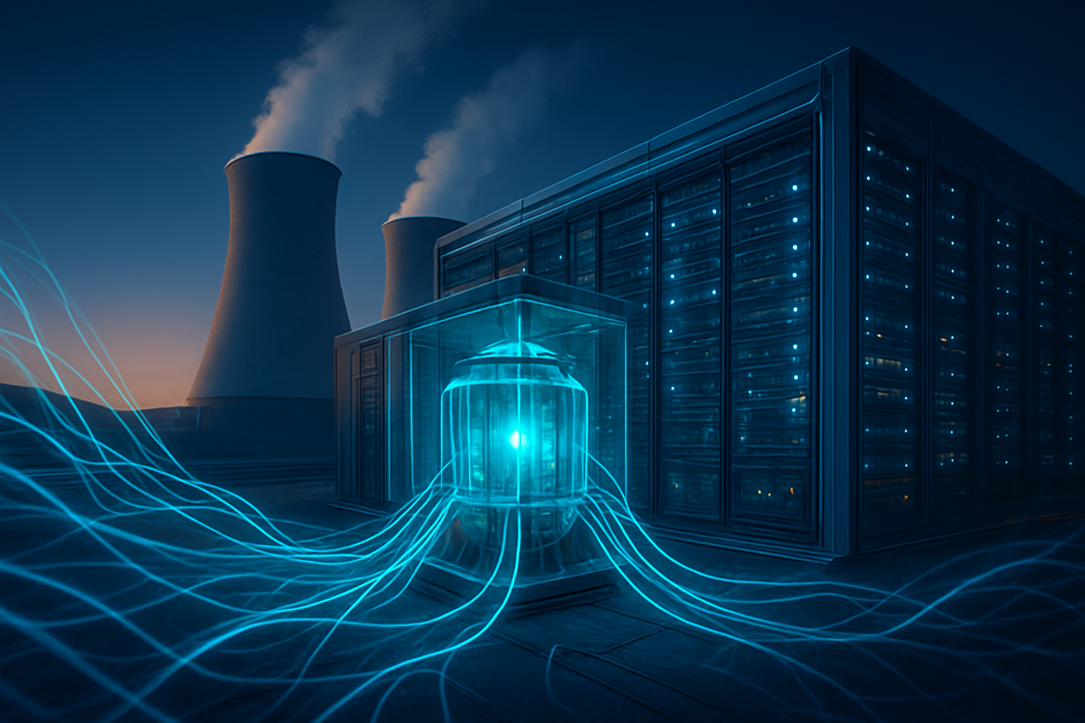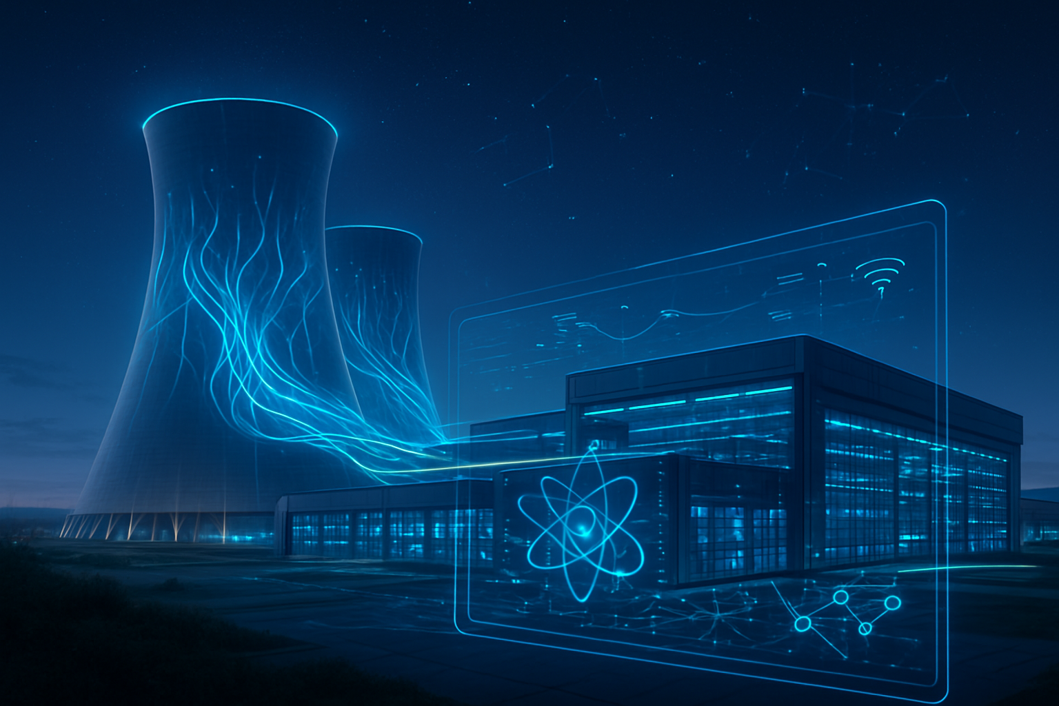
The global race for artificial intelligence supremacy has officially moved from the silicon of the microchip to the uranium of the reactor. As of February 2026, the tech industry has undergone a fundamental transformation, shifting its focus from software optimization to the securing of massive, 24/7 carbon-free energy (CFE) sources. At the heart of this movement is a historic resurgence of nuclear power, catalyzed by a series of landmark deals between "Hyperscalers" and energy providers that have effectively tethered the future of AI to the split atom.
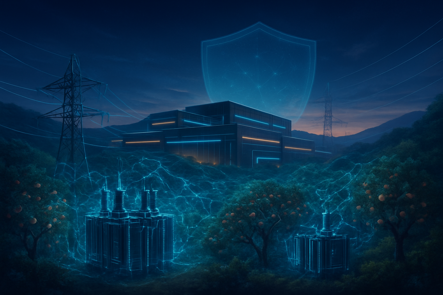
The immediate significance of this shift cannot be overstated. With the energy requirements for training and—more importantly—running inference for next-generation "reasoning" models skyrocketing, the traditional energy grid has reached a breaking point. By securing dedicated nuclear baseload, companies like Microsoft Corp. (NASDAQ: MSFT), Alphabet Inc. (NASDAQ: GOOGL), and Amazon.com, Inc. (NASDAQ: AMZN) are not just fueling their data centers; they are building a physical "energy moat" that may define the competitive landscape of the next decade.
The Resurrection of Three Mile Island and the Rise of the Crane Center
The most symbolic milestone in this energy pivot is the ongoing transformation of the infamous Three Mile Island Unit 1. Following a historic 20-year Power Purchase Agreement (PPA) signed in late 2024, Constellation Energy Corp. (NASDAQ: CEG) is currently in the final stages of restarting the facility, now officially renamed the Christopher M. Crane Clean Energy Center (CCEC). As of February 2026, the facility is approximately 80% staffed and has successfully passed critical NRC inspections of its steam generators. The project, bolstered by a $1 billion Department of Energy loan guarantee finalized in November 2025, is on track to deliver over 835 megawatts of carbon-free power to Microsoft’s regional data centers by early 2027.
Technically, this restart represents a departure from the "solar-plus-storage" strategies of the early 2020s. While renewables are cheaper per kilowatt-hour, their intermittent nature requires massive, expensive battery backups to support the 99.999% uptime required by AI clusters. Nuclear power provides a "capacity factor" of over 90%, offering a steady, high-density stream of electrons that matches the flat load profile of a GPU-dense data center. Initial reactions from the energy community have been largely positive, though some grid experts warn that the rapid "behind-the-meter" co-location of these centers could strain local transmission infrastructure.
Power as the New Moat: How Big Tech is Locking Up the Grid
The nuclear resurgence has created a widening chasm between the tech giants and smaller AI startups. In what analysts are calling "The Great Grid Capture," major players are effectively locking up the limited supply of existing nuclear assets. Beyond Microsoft’s deal, Amazon has finalized a massive 1,920 MW agreement with Talen Energy Corp. (NASDAQ: TLN) to draw power from the Susquehanna plant in Pennsylvania. Meanwhile, Google has secured a 25-year PPA with NextEra Energy, Inc. (NYSE: NEE) to restart the Duane Arnold Energy Center in Iowa, scheduled for 2029.
This land grab for baseload power provides a strategic advantage that goes beyond mere cost. By underwriting these multi-billion-dollar restarts and the development of Small Modular Reactors (SMRs), Hyperscalers are ensuring they have the headroom to scale while competitors are left waiting in years-long "interconnection queues." For a startup, the cost of entering a 20-year nuclear PPA is prohibitive, forcing them to rely on more volatile and expensive grid power. This physical constraint is becoming as significant as the scarcity of H100 or B200 GPUs was in previous years, effectively capping the growth of any entity without a direct line to a reactor.
The "Atoms for Algorithms" Consensus and the Inference Bottleneck
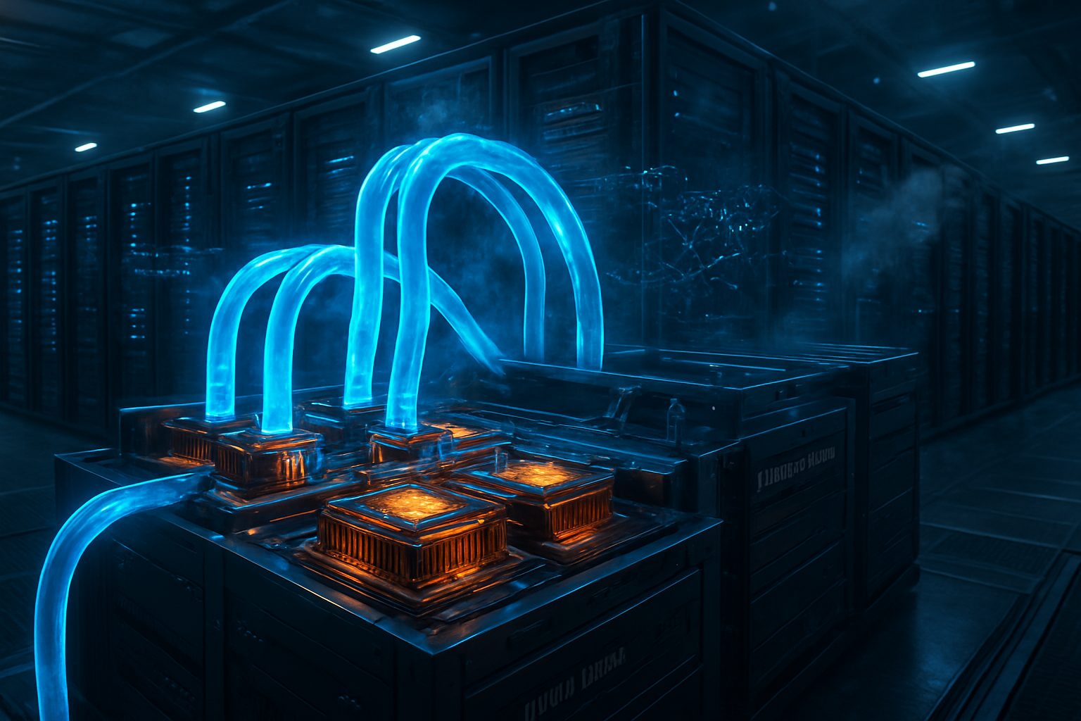
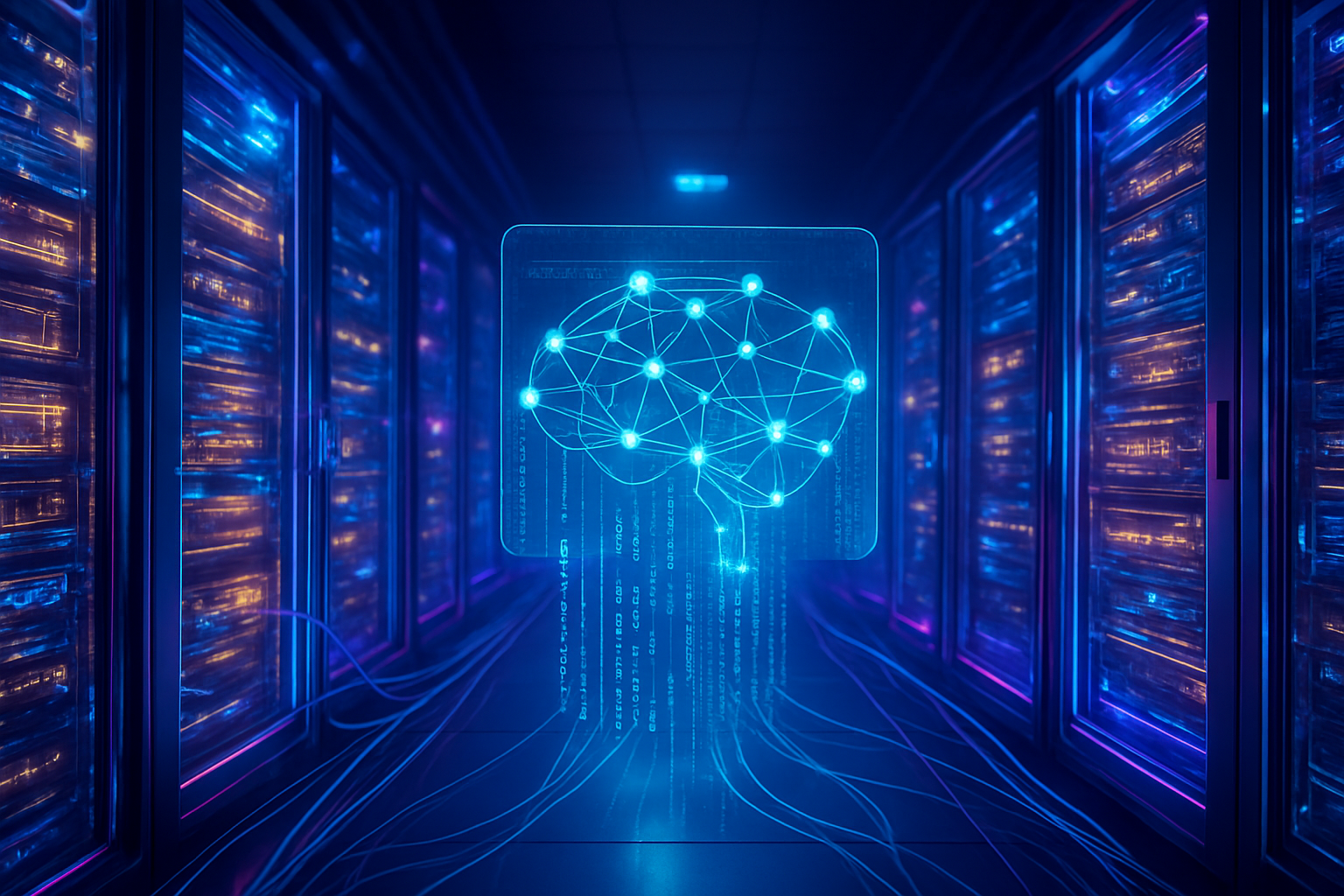
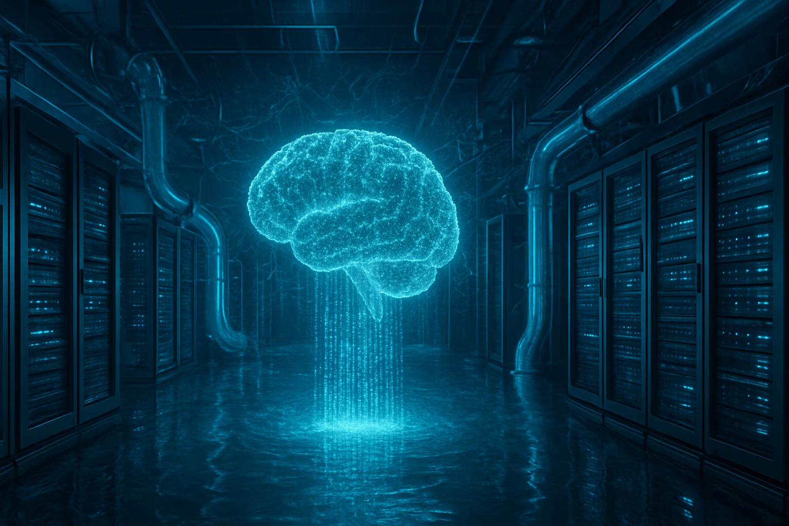
The broader significance of this trend lies in the realization that AI's energy hunger is even greater than initially projected. As of 2026, industry data shows that inference—the daily operation of AI models—now accounts for nearly 85% of total AI energy consumption. While training a frontier model might take 50 GWh, the daily inferencing of reasoning-heavy models (like the successors to OpenAI's o1 and o3) can consume tens of megawatt-hours every hour. To meet their net-zero commitments while deploying these energy-intensive "reasoning" agents, tech companies have been forced into a "nuclear-or-bust" paradigm.
This shift has also fundamentally altered the political and environmental landscape. The passage of the ADVANCE Act and subsequent executive orders in 2025 have streamlined reactor licensing to 18-month windows, framing nuclear energy as a matter of national AI competitiveness. However, this has led to a split in the environmental movement. While "Energy Abundance" advocates see this as the fastest way to decarbonize the grid, a coalition of over 200 environmental groups has raised concerns about the water consumption required for cooling these mega-data centers and the long-term management of nuclear waste.
Future Developments: SMRs and AI-Optimized Reactors
Looking ahead to 2030, the next phase of this resurgence will be the deployment of Small Modular Reactors (SMRs). Google’s partnership with Kairos Power is a bellwether for this trend; the first safety-related concrete for the "Hermes" demonstration reactor was poured in May 2025, and the company is now finalizing contracts for HALEU (High-Assay Low-Enriched Uranium) fuel. These smaller, factory-built reactors promise to be safer and more flexible than the aging behemoths of the 20th century, potentially allowing data centers to be built in locations previously unsuited for large-scale power plants.
The synergy between the two industries is also becoming circular. AI is now being used to optimize nuclear operations, with predictive maintenance algorithms reducing downtime and generative AI aiding in the complex design and licensing of new reactor cores. The challenge remains the supply chain for nuclear fuel and the workforce needed to operate these plants, but experts predict that the "nuclear-AI" hybrid will become the standard architecture for industrial computing by the end of the decade.
A New Era of Industrial Computing
The convergence of artificial intelligence and nuclear energy marks a defining chapter in the history of technology. What began as a search for sustainable power has evolved into a full-scale industrial re-alignment. The restart of Three Mile Island and the massive investments in SMRs by Google and Amazon represent a bet that the future of intelligence is inextricably linked to our ability to harness the most energy-dense source available to humanity.
In the coming months, the industry will be watching the final commissioning phases of the Crane Clean Energy Center and the regulatory progress of the first wave of commercial SMRs. The success or failure of these projects will determine whether the AI revolution can maintain its current pace or if it will be throttled by the physical limits of the 20th-century grid. For now, the message from Big Tech is clear: the road to AGI is paved with atoms.
This content is intended for informational purposes only and represents analysis of current AI developments.
TokenRing AI delivers enterprise-grade solutions for multi-agent AI workflow orchestration, AI-powered development tools, and seamless remote collaboration platforms.
For more information, visit https://www.tokenring.ai/.