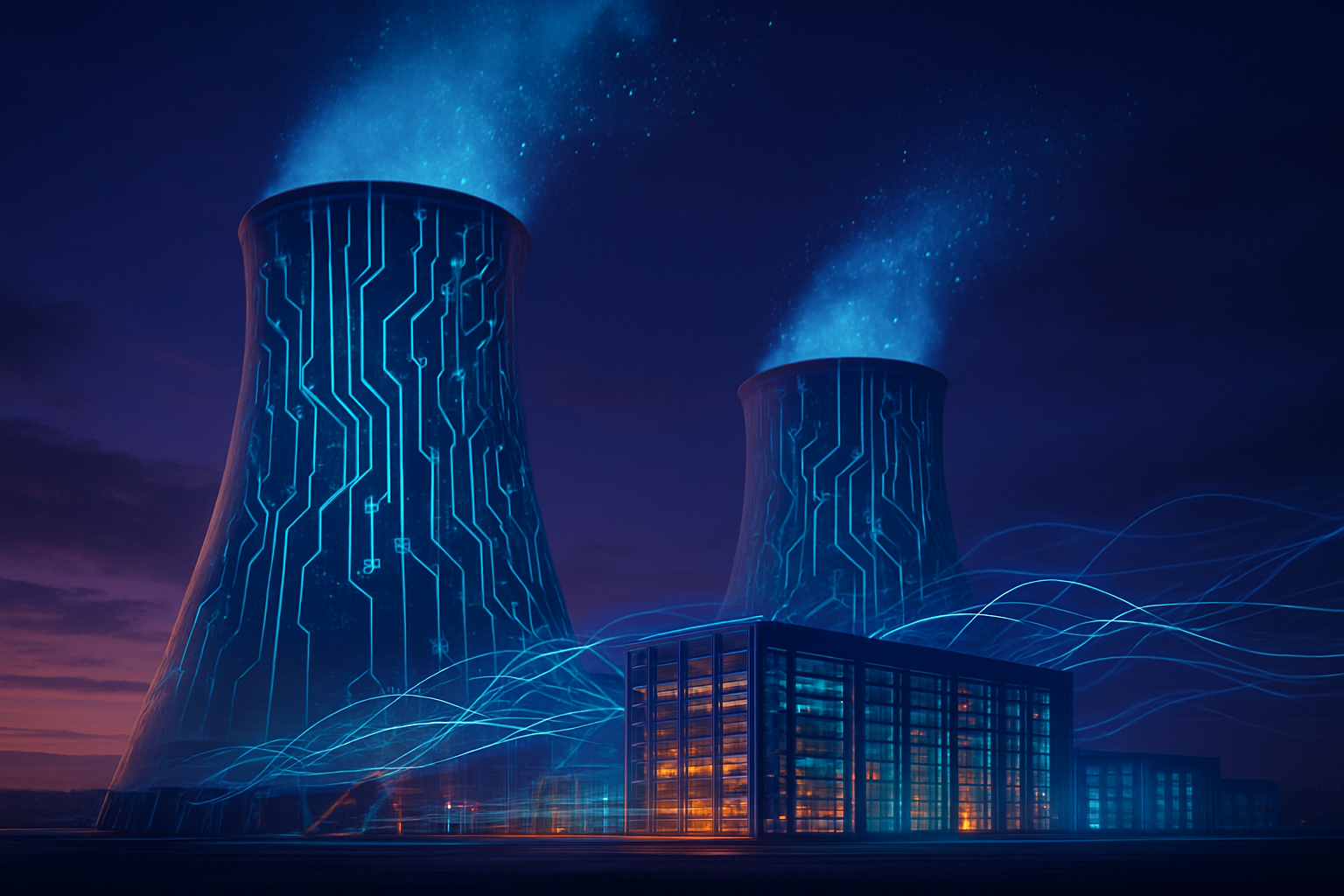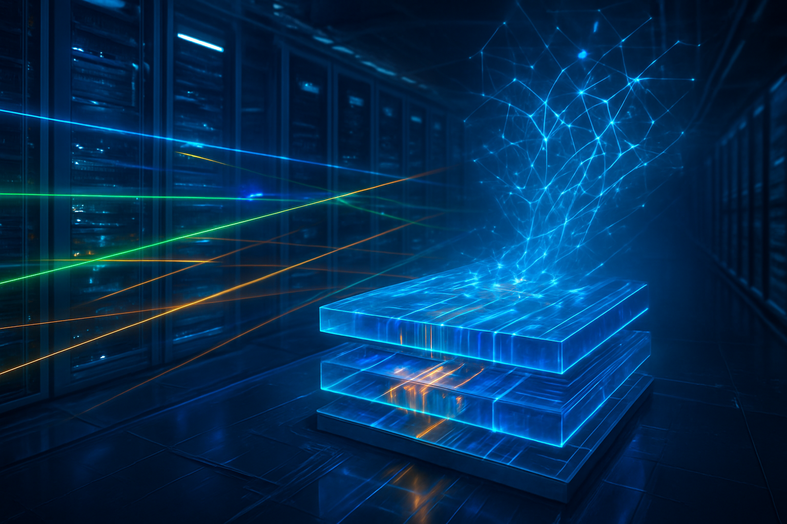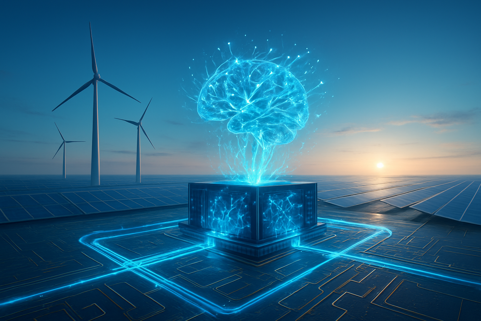
In a move that fundamentally redefines the relationship between Big Tech and the global energy grid, Brookfield Renewable Partners (NYSE: BEP) has entered into a series of unprecedented framework agreements to power the next generation of artificial intelligence. Headlining this green energy "land grab" is a massive 10.5-gigawatt (GW) deal with Microsoft Corp. (NASDAQ: MSFT), complemented by a multi-gigawatt hydropower expansion for Alphabet Inc. (NASDAQ: GOOGL). Valued at over $10 billion, this represents the largest corporate clean energy procurement in history, signaling that the bottleneck for AI supremacy has shifted from silicon chips to raw electrical power.
As of January 2026, the first contracts under these framework agreements are officially coming online, delivering carbon-free electricity to data centers across the United States and Europe. The scale is staggering: 10.5 GW is enough to power roughly 8 million homes or, more pivotally, to run dozens of the world’s most advanced AI training clusters. By securing this capacity through 2030, the tech giants are attempting to "future-proof" their AI ambitions against a backdrop of increasing grid instability and skyrocketing energy demand.
The 10.5 GW Framework: A New Blueprint for Infrastructure
The cornerstone of this development is the "Global Renewable Energy Framework Agreement" between Microsoft and Brookfield. Unlike traditional Power Purchase Agreements (PPAs), which typically focus on a single wind or solar farm, this framework provides a rolling pipeline of capacity to be delivered between 2026 and 2030. This ensures that as Microsoft scales its Azure AI infrastructure, the power is already accounted for, bypassing the years-long "interconnection queues" that currently plague the U.S. power grid.
Technically, the deal spans a diverse portfolio of assets, including onshore wind, utility-scale solar, and—increasingly—advanced "firm" power sources. To meet the 24/7 "always-on" requirements of AI workloads, Brookfield is leveraging its massive hydroelectric fleet. In early 2026, Google also began receiving its first deliveries from a separate 3 GW hydropower framework with Brookfield, specifically targeting the PJM Interconnection grid—the densest data center region in the world. This focus on "baseload" renewables is a critical evolution from earlier strategies that relied solely on intermittent solar and wind, which often required carbon-heavy backups when the sun went down.
Industry experts note that this deal is more than a simple purchase; it is a co-investment in the grid's modernization. The agreement includes provisions for "impactful carbon-free energy generation technologies," which analysts believe could eventually include long-duration battery storage and even small modular reactors (SMRs). The sheer volume of the investment—estimated between $10 billion and $11.5 billion for the Microsoft portion alone—provides Brookfield with the capital certainty to break ground on massive projects that would otherwise be deemed too risky for the merchant power market.
The Hyperscaler Arms Race: Who Benefits and Who is Left Behind?
The competitive implications of this deal are profound. By locking up 10.5 GW of Brookfield’s pipeline, Microsoft has effectively performed a "pre-emptive strike" on the renewable energy market. As AI models grow in complexity, the demand for power is expected to triple by 2030. Companies like Amazon.com Inc. (NASDAQ: AMZN) and Meta Platforms Inc. (NASDAQ: META) are now finding themselves in a fierce bidding war for the remaining "shovel-ready" renewable projects, potentially driving up the cost of green energy for non-tech industries.
Brookfield Renewable stands as the primary beneficiary of this trend, transitioning from a utility operator to a critical partner in the global AI supply chain. The deal has solidified Brookfield’s position as the world's largest developer of pure-play renewable power, with a total pipeline that now exceeds 200 GW. For Google and Microsoft, these deals are strategic shields against the "power bottleneck." By vertically integrating their energy supply chains, they reduce their exposure to volatile spot-market electricity prices and ensure their AI services—from Gemini to Copilot—can remain operational even as the grid reaches its limits.
However, the "crowding out" effect is a growing concern for smaller AI startups and traditional enterprises. As hyperscalers secure the vast majority of new renewable capacity, smaller players may be forced to rely on aging, fossil-fuel-dependent grids, potentially jeopardizing their ESG (Environmental, Social, and Governance) targets or facing higher operational costs that make their AI products less competitive.
AI’s Energy Hunger and the Global Significance
This $10 billion+ investment underscores a sobering reality: the AI revolution is an industrial-scale energy event. A single query to a generative AI model can consume ten times the electricity of a standard Google search. When multiplied by billions of users and the training of massive models like GPT-5 or Gemini 2, the energy requirements are astronomical. This deal marks the moment the tech industry moved beyond "carbon offsets" to "direct physical delivery" of green energy.
The broader significance lies in how this fits into the global energy transition. Critics have long argued that AI would derail climate goals by keeping coal and gas plants online to meet surging demand. The Brookfield deal provides a counter-narrative, suggesting that the massive capital of Big Tech can be the primary catalyst for the largest green infrastructure build-out in human history. It mirrors the 19th-century railway boom, where private capital built the foundational infrastructure that eventually benefited the entire economy.
There are, however, potential concerns. Grid operators are increasingly worried about the "data center density" in regions like Northern Virginia and Dublin. By injecting over 10 GW of demand into specific nodes, Microsoft and Google are testing the physical limits of high-voltage transmission lines. While the energy is "clean," the sheer volume of power moving through the system requires a complete overhaul of the physical wires and transformers that define the modern world.
The Road Ahead: 24/7 Carbon-Free Energy and Beyond
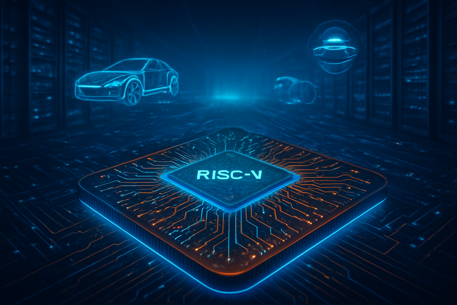
Looking toward the late 2020s, the "framework model" pioneered by Brookfield and Microsoft is expected to become the industry standard. We are likely to see similar multi-gigawatt deals announced involving advanced nuclear energy and deep-earth geothermal projects. In fact, the Global AI Infrastructure Investment Partnership (GAIIP)—a coalition including Microsoft, Nvidia Corp. (NASDAQ: NVDA), and BlackRock—is already aiming to mobilize $100 billion to expand this infrastructure even further.
The next frontier for these deals will be "temporal matching," where every kilowatt-hour consumed by a data center is matched in real-time by a carbon-free source. This will necessitate a massive expansion in long-duration energy storage (LDES). Experts predict that by 2028, the "Big Three" hyperscalers will likely own more power generation capacity than many mid-sized nations, effectively operating as private utilities that happen to provide cloud services on the side.
Wrapping Up: A Landmark in AI History
The 10.5 GW Brookfield deal is a watershed moment that proves the AI boom is as much about physical infrastructure as it is about software. It represents a $10 billion bet that the clean energy transition can keep pace with the exponential growth of artificial intelligence.
Key takeaways include:
- Infrastructure is King: AI scaling is now limited by energy and cooling, not just GPUs.
- Scale Matters: The shift from individual projects to multi-gigawatt "frameworks" allows for faster deployment of capital and cleaner energy.
- Strategic Advantage: Microsoft and Google are using their balance sheets to secure a competitive edge in power, which may become the most valuable commodity of the 21st century.
As we move through 2026, the industry will be watching the "interconnection speed"—how fast Brookfield can actually build these projects to match the blistering pace of AI hardware cycles. The success of this deal will determine whether the AI revolution will be remembered as a green industrial renaissance or a strain on the world’s most critical resource.
This content is intended for informational purposes only and represents analysis of current AI developments.
TokenRing AI delivers enterprise-grade solutions for multi-agent AI workflow orchestration, AI-powered development tools, and seamless remote collaboration platforms.
For more information, visit https://www.tokenring.ai/.