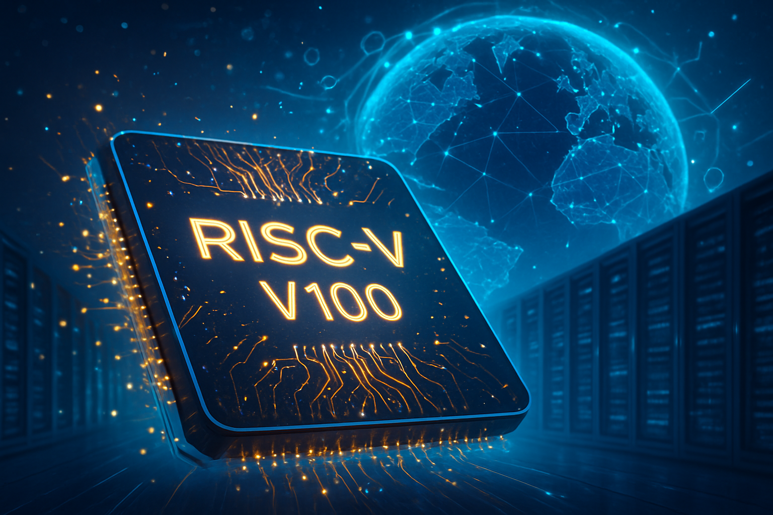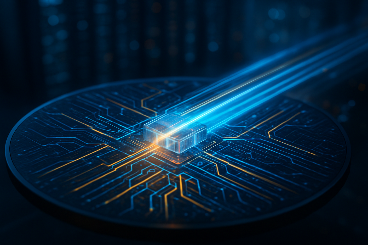
As the calendar turns to early 2026, the global semiconductor landscape is witnessing a tectonic shift that many industry veterans once thought impossible. The open-source RISC-V architecture, long relegated to low-power microcontrollers and experimental academia, has officially graduated to the data center. This week, the Hangzhou-based startup SpacemiT made waves across the industry with the formal launch of its Vital Stone V100, a 64-core server-class processor that represents the most aggressive challenge yet to the duopoly of x86 and the licensing hegemony of ARM.
This development serves as a realization of Item 18 on our 2026 Top 25 Technology Forecast: the "Massive Migration to Open-Source Silicon." The Vital Stone V100 is not merely another chip; it is the physical manifestation of a global movement toward "Silicon Sovereignty." By leveraging the RVA23 profile—the current gold standard for 64-bit application processors—SpacemiT is proving that the open-source community can deliver high-performance, secure, and AI-optimized hardware that rivals established proprietary giants.
The Technical Leap: Breaking the Performance Ceiling
The Vital Stone V100 is built on SpacemiT’s proprietary X100 core, featuring a high-density 64-core interconnect designed for the rigorous demands of modern cloud computing. Manufactured on a 12nm-class process, the V100 achieves a single-core performance of over 9 points/GHz on the SPECINT2006 benchmark. While this raw performance may not yet unseat the absolute highest-end chips from Intel Corporation (NASDAQ: INTC) or Advanced Micro Devices, Inc. (NASDAQ: AMD), it offers a staggering 30% advantage in performance-per-watt for specific AI-heavy and edge-computing workloads.
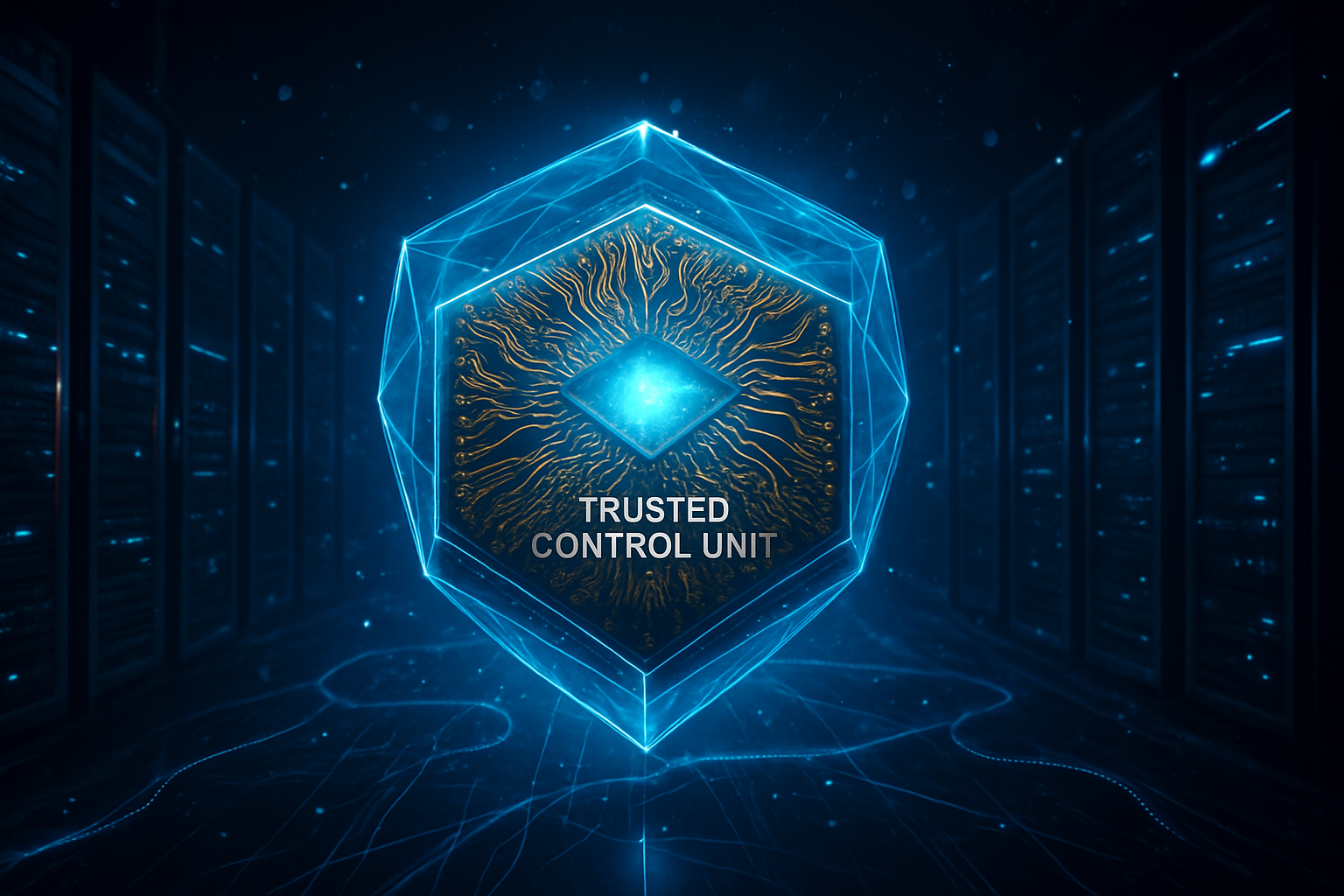
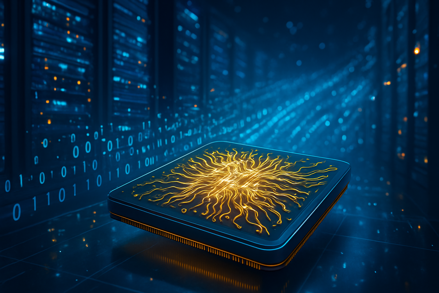
What truly distinguishes the V100 from its predecessors is its "fusion" architecture. The chip integrates Vector 1.0 extensions alongside 16 proprietary AI instructions specifically tuned for matrix multiplication and Large Language Model (LLM) acceleration. This makes the V100 a formidable contender for inference tasks in the data center. Furthermore, SpacemiT has incorporated full hardware virtualization support (Hypervisor 1.0, AIA 1.0, and IOMMU) and robust Reliability, Availability, and Serviceability (RAS) features—critical requirements for enterprise-grade server environments that previous RISC-V designs lacked.
Initial reactions from the AI research community have been overwhelmingly positive. Dr. Elena Vance, a senior hardware analyst, noted that "the V100 is the first RISC-V chip that doesn't ask you to compromise on modern software compatibility." By adhering to the RVA23 standard, SpacemiT ensures that standard Linux distributions and containerized workloads can run with minimal porting effort, bridging the gap that has historically kept open-source hardware out of the mainstream enterprise.
Strategic Realignment: A Threat to the ARM and x86 Status Quo
The arrival of the Vital Stone V100 sends a clear signal to the industry’s incumbents. For companies like Qualcomm Incorporated (NASDAQ: QCOM) and Meta Platforms, Inc. (NASDAQ: META), the rise of high-performance RISC-V provides a vital strategic hedge. By moving toward an open architecture, these tech giants can effectively eliminate the "ARM tax"—the substantial licensing and royalty fees paid to ARM Holdings—while simultaneously mitigating the risks associated with geopolitical trade tensions and export controls.
Hyperscalers such as Alphabet Inc. (NASDAQ: GOOGL) are particularly well-positioned to benefit from this shift. The ability to customize a RISC-V core without asking for permission from a proprietary gatekeeper allows these companies to build bespoke silicon tailored to their specific AI workloads. SpacemiT's success validates this "do-it-yourself" hardware strategy, potentially turning what were once customers of Intel and AMD into self-sufficient silicon designers.
Moreover, the competitive implications for the server market are profound. As RISC-V reaches 25% market penetration in late 2025 and moves toward a $52 billion annual valuation, the pressure on proprietary vendors to lower costs or drastically increase innovation is reaching a boiling point. The V100 isn't just a competitor to ARM’s Neoverse; it is an existential threat to the very idea that a single company should control the instruction set architecture (ISA) of the world’s servers.
Geopolitics and the Open-Source Renaissance
The broader significance of SpacemiT’s V100 cannot be understated in the context of the current geopolitical climate. As nations strive for technological independence, RISC-V has become the cornerstone of "Silicon Sovereignty." For China and parts of the European Union, adopting an open-source ISA is a way to bypass Western proprietary restrictions and ensure that their critical infrastructure remains free from foreign gatekeepers. This fits into the larger 2026 trend of "Geopatriation," where tech stacks are increasingly localized and sovereign.
This milestone is often compared to the rise of Linux in the 1990s. Just as Linux disrupted the proprietary operating system market by providing a free, collaborative alternative to Windows and Unix, RISC-V is doing the same for hardware. The V100 represents the "Linux 2.0" moment for silicon—the point where the open-source alternative is no longer just a hobbyist project but a viable enterprise solution.
However, this transition is not without its concerns. Some industry experts worry about the fragmentation of the RISC-V ecosystem. While standards like RVA23 aim to unify the platform, the inclusion of proprietary AI instructions by companies like SpacemiT could lead to a "Balkanization" of hardware, where software optimized for one RISC-V chip fails to run efficiently on another. Balancing innovation with standardization remains the primary challenge for the RISC-V International governing body.
The Horizon: What Lies Ahead for Open-Source Silicon
Looking forward, the momentum generated by SpacemiT is expected to trigger a cascade of new high-performance RISC-V announcements throughout late 2026. Experts predict that we will soon see the "brawny" cores from Tenstorrent, led by industry legend Jim Keller, matching the performance of AMD’s Zen 5 and ARM’s Neoverse V3. This will further solidify RISC-V’s place in the high-performance computing (HPC) and AI training sectors.
In the near term, we expect to see the Vital Stone V100 deployed in small-scale data center clusters by the fourth quarter of 2026. These early deployments will serve as a proof-of-concept for larger cloud service providers. The next frontier for RISC-V will be the integration of advanced chiplet architectures, allowing companies to mix and match SpacemiT cores with specialized accelerators from other vendors, creating a truly modular and open ecosystem.
The ultimate challenge will be the software. While the hardware is ready, the ecosystem of compilers, libraries, and debuggers must continue to mature. Analysts predict that by 2027, the "RISC-V first" software development mentality will become common, as developers seek to target the most flexible and cost-effective hardware available.
A New Era of Computing
The launch of SpacemiT’s Vital Stone V100 is more than a product release; it is a declaration of independence for the semiconductor industry. By proving that a 64-core, server-class processor can be built on an open-source foundation, SpacemiT has shattered the glass ceiling for RISC-V. This development confirms the transition of RISC-V from an experimental architecture to a pillar of the global digital economy.
Key takeaways from this announcement include the achievement of performance parity in specific power-constrained workloads, the strategic pivot of major tech giants away from proprietary licensing, and the role of RISC-V in the quest for national technological sovereignty. As we move into the latter half of 2026, the industry will be watching closely to see how the "Big Three"—Intel, AMD, and ARM—respond to this unprecedented challenge.
The "Open-Source Architecture Revolution," as highlighted in our Top 25 list, is no longer a future prediction; it is our current reality. The walls of the proprietary garden are coming down, and in their place, a more diverse, competitive, and innovative silicon landscape is taking root.
This content is intended for informational purposes only and represents analysis of current AI developments.
TokenRing AI delivers enterprise-grade solutions for multi-agent AI workflow orchestration, AI-powered development tools, and seamless remote collaboration platforms.
For more information, visit https://www.tokenring.ai/.