Tag: Data Centers

  • Light-Speed AI: Marvell’s $5.5B Bet on Celestial AI Signals the End of the “Memory Wall”

    Light-Speed AI: Marvell’s $5.5B Bet on Celestial AI Signals the End of the “Memory Wall”

    In a move that signals a fundamental shift in the architecture of artificial intelligence, Marvell Technology (NASDAQ: MRVL) has announced the definitive acquisition of Celestial AI, a leader in optical interconnect technology. The deal, valued at up to $5.5 billion, represents the most significant attempt to date to replace traditional copper-based electrical signals with light-based photonic communication within the data center. By integrating Celestial AI’s "Photonic Fabric" into its portfolio, Marvell is positioning itself at the center of the industry’s desperate push to solve the "memory wall"—the bottleneck where the speed of processors outpaces the ability to move data from memory.

    The acquisition comes at a critical juncture for the semiconductor industry. As of January 22, 2026, the demand for massive AI models has pushed existing hardware to its physical limits. Traditional electrical interconnects, which rely on copper traces to move data between GPUs and High-Bandwidth Memory (HBM), are struggling with heat, power consumption, and physical distance constraints. Marvell’s absorption of Celestial AI, combined with its recent $540 million purchase of XConn Technologies, suggests that the future of AI scaling will not be built on faster electrons, but on the seamless integration of silicon photonics and memory disaggregation.

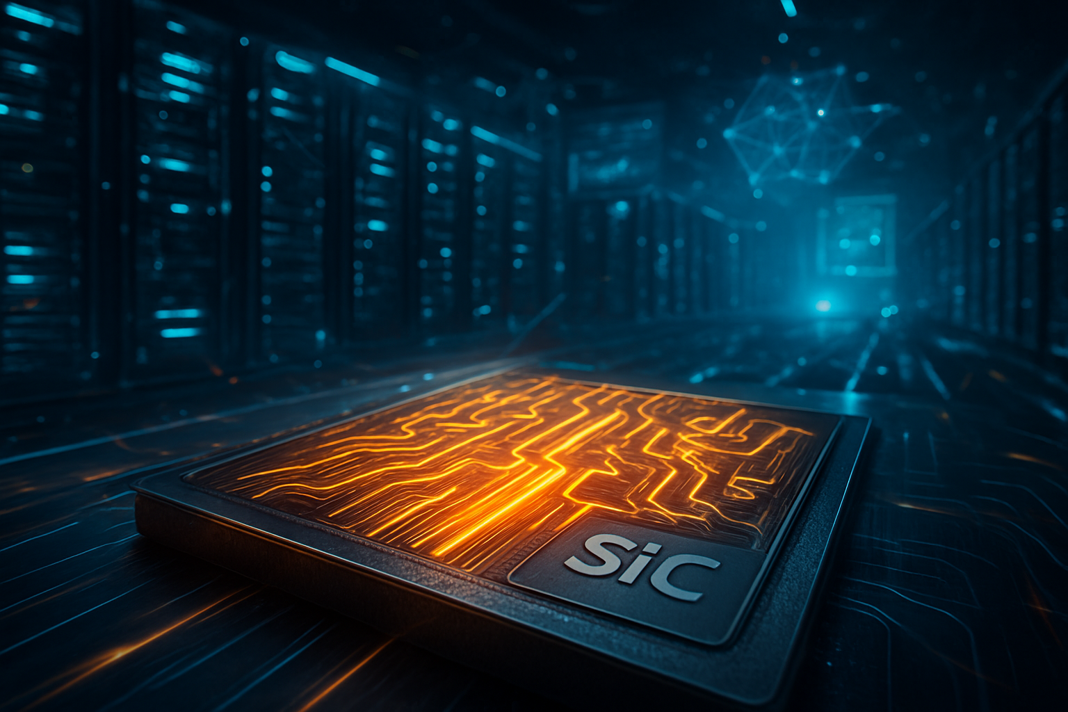
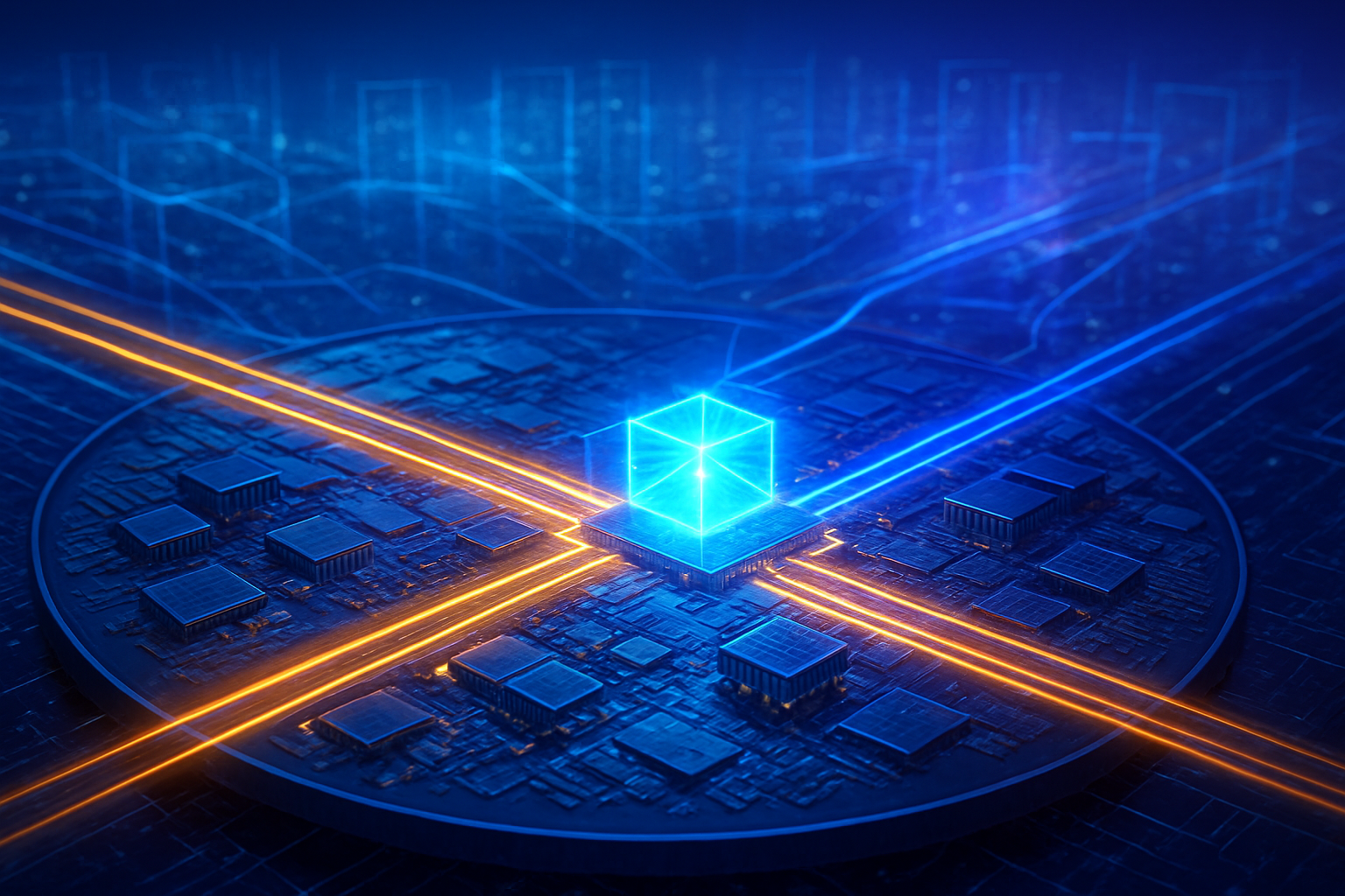
    The Photonic Fabric: Technical Mastery Over the Memory Bottleneck

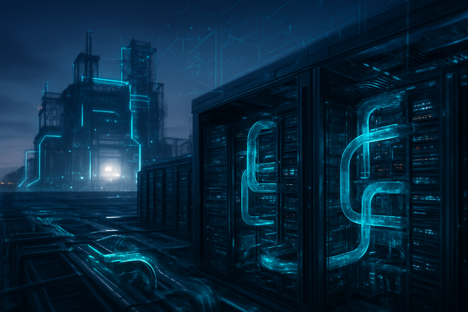
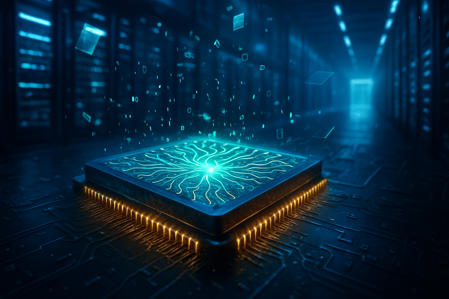
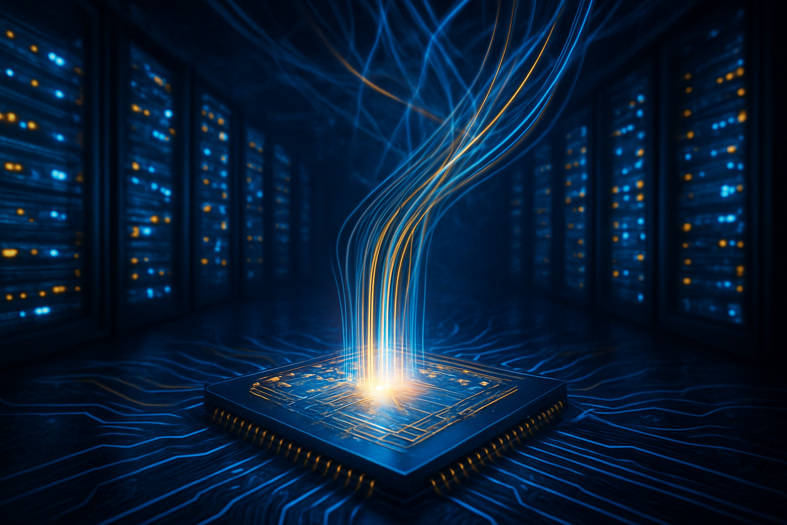
    The centerpiece of this acquisition is Celestial AI’s proprietary Photonic Fabric™, an optical interconnect platform that achieves what was previously thought impossible: 3D-stacked optical I/O directly on the compute die. Unlike traditional silicon photonics that use temperature-sensitive ring modulators, Celestial AI utilizes Electro-Absorption Modulators (EAMs). These components are remarkably thermally stable, allowing photonic chiplets to be co-packaged alongside high-power AI accelerators (XPUs) that can generate several kilowatts of heat. This technical leap allows for a 10x increase in bandwidth density, with first-generation chiplets delivering a staggering 16 terabits per second (Tbps) of throughput.

    Perhaps the most disruptive aspect of the Photonic Fabric is its "DSP-free" analog-equalized linear-drive architecture. By eliminating the need for complex Digital Signal Processors (DSPs) to clean up electrical signals, the system reduces power consumption by an estimated 4 to 5 times compared to copper-based solutions. This efficiency enables a new architectural paradigm known as memory disaggregation. In this setup, High-Bandwidth Memory (HBM) no longer needs to be soldered within millimeters of the processor. Marvell’s roadmap now includes "Photonic Fabric Appliances" (PFAs) capable of pooling up to 32 terabytes of HBM3E or HBM4 memory, accessible to hundreds of XPUs across a distance of up to 50 meters with nanosecond-class latency.

    The industry reaction has been one of cautious optimism followed by rapid alignment. Experts in the AI research community note that moving I/O from the "beachfront" (the edges) of a chip to the center of the die via 3D stacking frees up valuable perimeter space for even more HBM stacks. This effectively triples the on-chip memory capacity available to the processor. "We are moving from a world where we build bigger chips to a world where we build bigger systems connected by light," noted one lead architect at a major hyperscaler. The design win announced by Celestial AI just prior to the acquisition closure confirms that at least one Tier-1 cloud provider is already integrating this technology into its 2027 silicon roadmap.

    Reshaping the Competitive Landscape: Marvell, Broadcom, and the UALink War

    The acquisition sets up a titanic clash between Marvell (NASDAQ: MRVL) and Broadcom (NASDAQ: AVGO). While Broadcom has dominated the networking space with its Tomahawk and Jericho switch series, it has doubled down on "Scale-Up Ethernet" (SUE) and its "Davisson" 102.4 Tbps switch as the primary solution for AI clusters. Broadcom’s strategy emphasizes the maturity and reliability of Ethernet. In contrast, Marvell is betting on a more radical architectural shift. By combining Celestial AI’s optical physical layer with XConn’s CXL (Compute Express Link) and PCIe switching logic, Marvell is providing the "plumbing" for the newly finalized Ultra Accelerator Link (UALink) 1.0 specification.

    This puts Marvell in direct competition with NVIDIA (NASDAQ: NVDA). Currently, NVIDIA’s proprietary NVLink is the gold standard for high-speed GPU-to-GPU communication, but it remains a "walled garden." The UALink Consortium, which includes heavyweights like Advanced Micro Devices (NASDAQ: AMD), Intel (NASDAQ: INTC), Meta Platforms (NASDAQ: META), and Microsoft (NASDAQ: MSFT), is positioning Marvell’s new photonic capabilities as the "open" alternative to NVLink. For hyperscalers like Alphabet (NASDAQ: GOOGL) and Amazon (NASDAQ: AMZN), Marvell’s technology offers a path to build massive, multi-rack AI clusters that aren't beholden to NVIDIA’s full-stack pricing and hardware constraints.

    The market positioning here is strategic: Broadcom is the incumbent of "reliable connectivity," while Marvell is positioning itself as the architect of the "optical future." The acquisition of Celestial AI effectively gives Marvell a two-year lead in the commercialization of 3D-stacked optical I/O. If Marvell can successfully integrate these photonic chiplets into the UALink ecosystem by 2027, it could potentially displace Broadcom in the highest-performance tiers of the AI data center, especially as power delivery to traditional copper-based switches becomes an insurmountable engineering hurdle.

    A Post-Moore’s Law Reality: The Significance of Optical Scaling

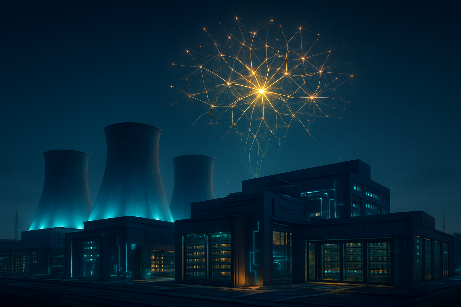
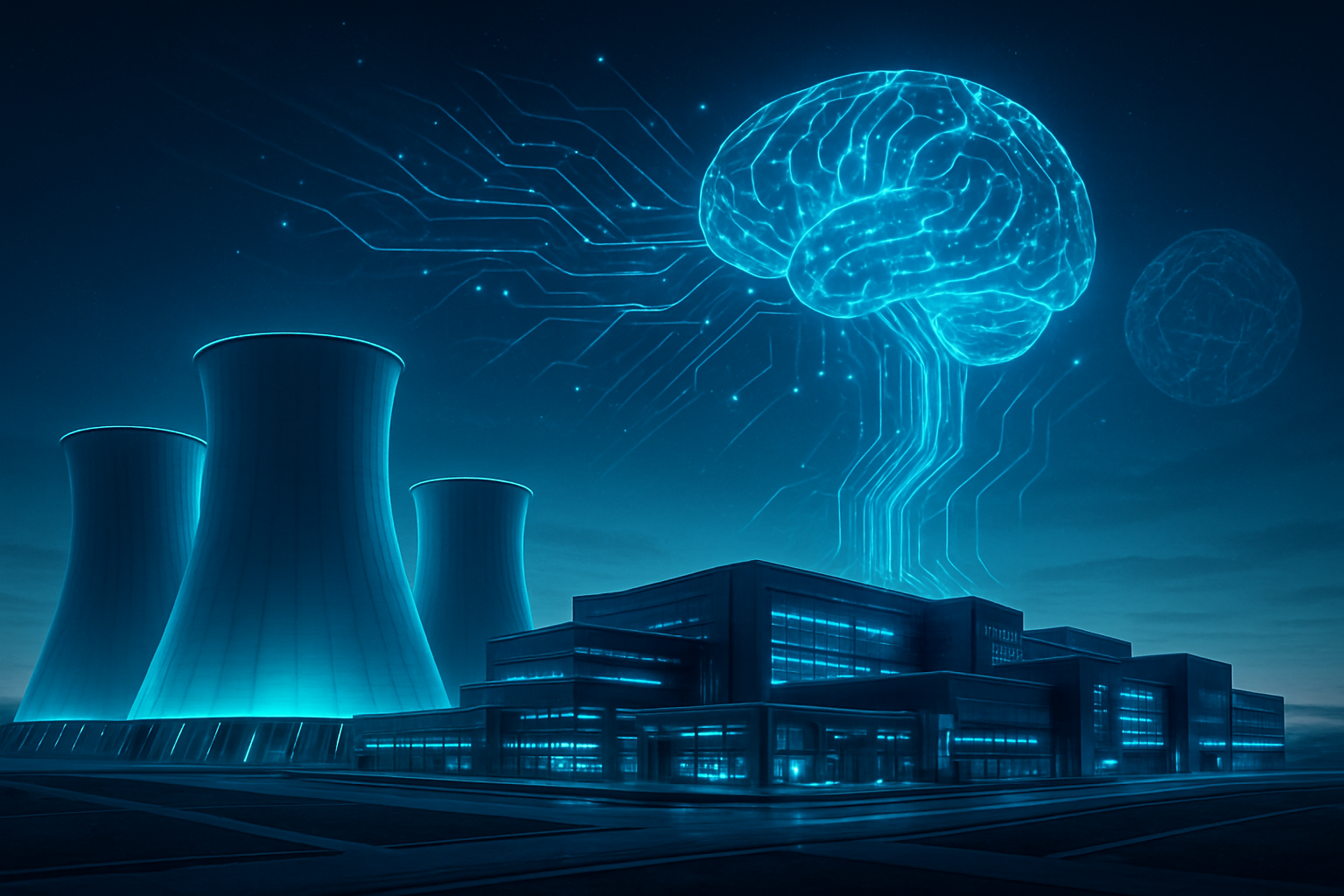
    Beyond the corporate maneuvering, this breakthrough represents a pivotal moment in the broader AI landscape. We are witnessing the twilight of Moore’s Law as defined by transistor density, and the dawn of a new era defined by "system-level scaling." As AI models like GPT-5 and its successors demand trillions of parameters, the energy required to move data between a processor and its memory has become the primary limit on intelligence. Marvell’s move to light-based interconnects addresses the energy crisis of the data center head-on, offering a way to keep scaling AI performance without requiring a dedicated nuclear power plant for every new cluster.

    Comparisons are already being made to previous milestones like the introduction of HBM or the first multi-chip module (MCM) designs. However, the shift to photons is arguably more fundamental. It represents the first time the "memory wall" has been physically dismantled rather than just temporarily bypassed. By allowing for "any-to-any" memory access across a fabric of light, researchers can begin to design AI architectures that are not constrained by the physical size of a single silicon wafer. This could lead to more efficient "sparse" AI models that leverage massive memory pools more effectively than the dense, compute-heavy models of today.

    However, concerns remain regarding the manufacturability and yield of 3D-stacked optical components. Integrating laser sources and modulators onto silicon at scale is a feat of extreme precision. Critics also point out that while the latency is "nanosecond-class," it is still higher than local on-chip SRAM. The industry will need to develop new software and compilers capable of managing these massive, disaggregated memory pools—a task that companies like Cisco (NASDAQ: CSCO) and HP Enterprise (NYSE: HPE) are already beginning to address through new software-defined networking standards.

    The Road Ahead: 2026 and Beyond

    In the near term, expect to see the first silicon "tape-outs" featuring Celestial AI’s technology by the end of 2026, with early-access samples reaching major cloud providers in early 2027. The immediate application will be "Memory Expansion Modules"—pluggable units that allow a single AI server to access terabytes of external memory at local speeds. Looking further out, the 2028-2029 timeframe will likely see the rise of the "Optical Rack," where the entire data center rack functions as a single, giant computer, with hundreds of GPUs sharing a unified memory space over a photonic backplane.

    The challenges ahead are largely related to the ecosystem. For Marvell to succeed, the UALink standard must gain universal adoption among chipmakers like Samsung (KRX: 005930) and SK Hynix, who will need to produce "optical-ready" HBM modules. Furthermore, the industry must solve the "laser problem"—deciding whether to integrate the light source directly into the chip (higher efficiency) or use external laser sources (higher reliability and easier replacement). Experts predict that the move toward external, field-replaceable laser modules will win out in the first generation to ensure data center uptime.

    Final Thoughts: A Luminous Horizon for AI

    The acquisition of Celestial AI by Marvell is more than just a business transaction; it is a declaration that the era of the "all-electrical" data center is coming to an end. As we look back from the perspective of early 2026, this event may well be remembered as the moment the industry finally broke the memory wall, paving the way for the next order of magnitude in artificial intelligence development.

    The long-term impact will be measured in the democratization of high-end AI compute. By providing an open, optical alternative to proprietary fabrics, Marvell is ensuring that the race for AGI remains a multi-player competition rather than a single-company monopoly. In the coming weeks, keep a close eye on the closing of the deal and any subsequent announcements from the UALink Consortium. The first successful demonstration of a 32TB photonic memory pool will be the signal that the age of light-speed computing has truly arrived.


    This content is intended for informational purposes only and represents analysis of current AI developments.

    TokenRing AI delivers enterprise-grade solutions for multi-agent AI workflow orchestration, AI-powered development tools, and seamless remote collaboration platforms.
    For more information, visit https://www.tokenring.ai/.


    Authored by: Expert Technology Journalist for TokenRing AI
    Current Date: January 22, 2026


    Note: Public companies mentioned include Marvell Technology (NASDAQ: MRVL), NVIDIA (NASDAQ: NVDA), Broadcom (NASDAQ: AVGO), Advanced Micro Devices (NASDAQ: AMD), Intel (NASDAQ: INTC), Meta Platforms (NASDAQ: META), Microsoft (NASDAQ: MSFT), Alphabet (NASDAQ: GOOGL), Amazon (NASDAQ: AMZN), Cisco (NASDAQ: CSCO), HP Enterprise (NYSE: HPE), and Samsung (KRX: 005930).

  • The Power War: Satya Nadella Warns Energy and Cooling are the Final Frontiers of AI

    The Power War: Satya Nadella Warns Energy and Cooling are the Final Frontiers of AI

    In a series of candid remarks delivered between the late 2025 earnings cycle and the recent 2026 World Economic Forum in Davos, Microsoft (NASDAQ:MSFT) CEO Satya Nadella has signaled a fundamental shift in the artificial intelligence arms race. The era of the "chip shortage" has officially ended, replaced by a much more physical and daunting obstacle: the "Energy Wall." Nadella warned that the primary bottlenecks for AI scaling are no longer the availability of high-end silicon, but the skyrocketing costs of electricity and the lack of advanced liquid cooling infrastructure required to keep next-generation data centers from melting down.

    The significance of these comments cannot be overstated. For the past three years, the tech industry has focused almost exclusively on securing NVIDIA (NASDAQ:NVDA) H100 and Blackwell GPUs. However, Nadella’s admission that Microsoft currently holds a vast inventory of unutilized chips—simply because there isn't enough power to plug them in—marks a pivot from digital constraints to the limitations of 20th-century physical infrastructure. As the industry moves toward trillion-parameter models, the struggle for dominance has moved from the laboratory to the power grid.

    From Silicon Shortage to the "Warm Shell" Crisis

    Nadella’s technical diagnosis of the current AI landscape centers on the concept of the "warm shell"—a data center building that is fully permitted, connected to a high-voltage grid, and equipped with the specialized thermal management systems needed for modern compute densities. During a recent appearance on the BG2 Podcast, Nadella noted that Microsoft’s biggest challenge is no longer compute glut, but the "linear world" of utility permitting and power plant construction. While software can be iterated in weeks and chips can be fabricated in months, building a new substation or a high-voltage transmission line can take a decade.

    To circumvent these physical limits, Microsoft has begun a massive architectural overhaul of its global data center fleet. At the heart of this transition is the newly unveiled "Fairwater" architecture. Unlike traditional cloud data centers designed for 10-15 kW racks, Fairwater is built to support a staggering 140 kW per rack. This 10x increase in power density is necessitated by the latest AI chips, which generate heat far beyond the capabilities of traditional air-conditioning systems.

    To manage this thermal load, Microsoft is moving toward standardized, closed-loop liquid cooling. This system utilizes direct-to-chip microfluidics—a technology co-developed with Corintis that etches cooling channels directly onto the silicon. This approach reduces peak operating temperatures by as much as 65% while operating as a "zero-water" system. Once the initial coolant is loaded, the system recirculates indefinitely, addressing both the energy bottleneck and the growing public scrutiny over data center water consumption.

    The Competitive Shift: Vertical Integration or Gridlock

    This infrastructure bottleneck has forced a strategic recalibration among the "Big Five" hyperscalers. While Microsoft is doubling down on "Fairwater," its rivals are pursuing their own paths to energy independence. Alphabet (NASDAQ:GOOGL), for instance, recently closed a $4.75 billion acquisition of Intersect Power, allowing it to bypass the public grid by co-locating data centers directly with its own solar and battery farms. Meanwhile, Amazon (NASDAQ:AMZN) has pivoted toward a "nuclear renaissance," committing hundreds of millions of dollars to Small Modular Reactors (SMRs) through partnerships with X-energy.

    The competitive advantage in 2026 is no longer held by the company with the best model, but by the company that can actually power it. This shift favors legacy giants with the capital to fund multi-billion dollar grid upgrades. Microsoft’s "Community-First AI Infrastructure" initiative is a direct response to this, where the company effectively acts as a private utility, funding local substations and grid modernizations to secure the "social license" to operate.

    Startups and smaller AI labs face a growing disadvantage. While a boutique lab might raise the funds to buy a cluster of Blackwell chips, they lack the leverage to negotiate for 500 megawatts of power from local utilities. We are seeing a "land grab" for energized real estate, where the valuation of a data center site is now determined more by its proximity to a high-voltage line than by its proximity to a fiber-optic hub.

    Redefining the AI Landscape: The Energy-GDP Correlation

    Nadella’s comments fit into a broader trend where AI is increasingly viewed through the lens of national security and energy policy. At Davos 2026, Nadella argued that future GDP growth would be directly correlated to a nation’s energy costs associated with AI. If the "energy wall" remains unbreached, the cost of running an AI query could become prohibitively expensive, potentially stalling the much-hyped "AI-led productivity boom."

    The environmental implications are also coming to a head. The shift to liquid cooling is not just a technical necessity but a political one. By moving to closed-loop systems, Microsoft and Meta (NASDAQ:META) are attempting to mitigate the "water wall"—the local pushback against data centers that consume millions of gallons of water in drought-prone regions. However, the sheer electrical demand remains. Estimates suggest that by 2030, AI could consume upwards of 4% of total global electricity, a figure that has prompted some experts to compare the current AI infrastructure build-out to the expansion of the interstate highway system or the electrification of the rural South.

    The Road Ahead: Fusion, Fission, and Efficiency

    Looking toward late 2026 and 2027, the industry is betting on radical new energy sources to break the bottleneck. Microsoft has already signed a power purchase agreement with Helion Energy for fusion power, a move that was once seen as science fiction but is now viewed as a strategic necessity. In the near term, we expect to see more "behind-the-meter" deployments where data centers are built on the sites of retired coal or nuclear plants, utilizing existing transmission infrastructure to shave years off deployment timelines.

    On the cooling front, the next frontier is "immersion cooling," where entire server racks are submerged in non-conductive dielectric fluid. While Microsoft’s current Fairwater design uses direct-to-chip liquid cooling, industry experts predict that the 200 kW racks of the late 2020s will require full immersion. This will necessitate an even deeper partnership with cooling specialized firms like LG Electronics (KRX:066570), which recently signed a multi-billion dollar deal to supply Microsoft’s global cooling stack.

    Summary: The Physical Reality of Intelligence

    Satya Nadella’s recent warnings serve as a reality check for an industry that has long lived in the realm of virtual bits and bytes. The realization that thousands of world-class GPUs are sitting idle in warehouses for lack of a "warm shell" is a sobering milestone in AI history. It signals that the easy gains from software optimization are being met by the hard realities of thermodynamics and aging electrical grids.

    As we move deeper into 2026, the key metrics to watch will not be benchmark scores or parameter counts, but "megawatts under management" and "coolant efficiency ratios." The companies that successfully bridge the gap between AI's infinite digital potential and the Earth's finite physical resources will be the ones that define the next decade of technology.


    This content is intended for informational purposes only and represents analysis of current AI developments.

    TokenRing AI delivers enterprise-grade solutions for multi-agent AI workflow orchestration, AI-powered development tools, and seamless remote collaboration platforms.
    For more information, visit https://www.tokenring.ai/.

  • The Speed of Light: Silicon Photonics and CPO Emerge as the Backbone of the ‘Million-GPU’ AI Power Grid

    The Speed of Light: Silicon Photonics and CPO Emerge as the Backbone of the ‘Million-GPU’ AI Power Grid

    As of January 2026, the artificial intelligence industry has reached a pivotal physical threshold. For years, the scaling of large language models was limited by compute density and memory capacity. Today, however, the primary bottleneck has shifted to the "Energy Wall"—the staggering amount of power required simply to move data between processors. To shatter this barrier, the semiconductor industry is undergoing its most significant architectural shift in a decade: the transition from copper-based electrical signaling to light-based interconnects. Silicon Photonics and Co-Packaged Optics (CPO) are no longer experimental concepts; they have become the critical infrastructure, or the "backbone," of the modern AI power grid.

    The significance of this transition cannot be overstated. As hyperscalers race toward building "million-GPU" clusters to train the next generation of Artificial General Intelligence (AGI), the traditional "I/O tax"—the energy consumed by data moving across a data center—has threatened to stall progress. By integrating optical engines directly onto the chip package, companies are now able to reduce data-transfer energy consumption by up to 70%, effectively redirecting megawatts of power back into actual computation. This month marks a major milestone in this journey, as the industry’s biggest players, including TSMC (NYSE: TSM), Broadcom (NASDAQ: AVGO), and Ayar Labs, unveil the production-ready hardware that will define the AI landscape for the next five years.

    Breaking the Copper Wall: Technical Foundations of 2026

    The technical heart of this revolution lies in the move from pluggable transceivers to Co-Packaged Optics. Leading the charge is Taiwan Semiconductor Manufacturing Company (TPE: 2330), whose Compact Universal Photonic Engine (COUPE) technology has entered its final production validation phase this January, with full-scale mass production slated for the second half of 2026. COUPE utilizes TSMC’s proprietary SoIC-X (System on Integrated Chips) 3D-stacking technology to place an Electronic Integrated Circuit (EIC) directly on top of a Photonic Integrated Circuit (PIC). This configuration eliminates the parasitic capacitance of traditional wiring, supporting staggering bandwidths of 1.6 Tbps in its first generation, with a roadmap toward 12.8 Tbps by 2028.

    Simultaneously, Broadcom (NASDAQ: AVGO) has begun shipping pilot units of its Gen 3 CPO platform, powered by the Tomahawk 6 (code-named "Davisson") switch silicon. This generation introduces 200 Gbps per lane optical connectivity, enabling the construction of 102.4 Tbps Ethernet switches. Unlike previous iterations, Broadcom’s Gen 3 removes the power-hungry Digital Signal Processor (DSP) from the optical module, utilizing a "direct drive" architecture that slashes latency to under 10 nanoseconds. This is critical for the "scale-up" fabrics required by NVIDIA (NASDAQ: NVDA) and AMD (NASDAQ: AMD), where thousands of GPUs must act as a single, massive processor without the lag inherent in traditional networking.

    Further diversifying the ecosystem is the partnership between Ayar Labs and Global Unichip Corp (TPE: 3443). The duo has successfully integrated Ayar Labs’ TeraPHY™ optical engines into GUC’s advanced ASIC design workflow. Using the Universal Chiplet Interconnect Express (UCIe) standard, they have achieved a "shoreline density" of 1.4 Tbps/mm², allowing more than 100 Tbps of aggregate bandwidth from a single processor package. This approach solves the mechanical and thermal challenges of CPO by using specialized "stiffener" designs and detachable fiber connectors, making light-based I/O accessible for custom AI accelerators beyond just the major GPU vendors.

    A New Competitive Frontier for Hyperscalers and Chipmakers

    The shift to silicon photonics creates a clear divide between those who can master light-based interconnects and those who cannot. For major AI labs and hyperscalers like Google (NASDAQ: GOOGL) and Meta (NASDAQ: META), this technology is the "buy" that allows them to scale their data centers from single buildings to entire "AI Factories." By reducing the "I/O tax" from 20 picojoules per bit (pJ/bit) to less than 5 pJ/bit, these companies can operate much larger clusters within the same power envelope, providing a massive strategic advantage in the race for AGI.

    NVIDIA and AMD are the most immediate beneficiaries. NVIDIA is already preparing its "Rubin Ultra" platform to integrate TSMC’s COUPE technology, ensuring its leadership in the "scale-up" domain where low-latency communication is king. Meanwhile, Broadcom’s dominance in the networking fabric allows it to act as the primary "toll booth" for the AI power grid. For startups, the Ayar Labs and GUC partnership is a game-changer; it provides a standardized, validated path to integrate optical I/O into bespoke AI silicon, potentially disrupting the dominance of off-the-shelf GPUs by allowing specialized chips to communicate at speeds previously reserved for top-tier hardware.

    However, this transition is not without risk. The move to CPO disrupts the traditional "pluggable" optics market, long dominated by specialized module makers. As optical engines move onto the chip package, the traditional supply chain is being compressed, forcing many optics companies to either partner with foundries or face obsolescence. The market positioning of TSMC as a "one-stop shop" for both logic and photonics packaging further consolidates power in the hands of the world's largest foundry, raising questions about future supply chain resilience.

    Lighting the Way to AGI: Wider Significance

    The rise of silicon photonics represents more than just a faster way to move data; it is a fundamental shift in the AI landscape. In the era of the "Copper Wall," physical distance was a dealbreaker—high-speed electrical signals could only travel about a meter before degrading. This limited AI clusters to single racks or small rows. Silicon photonics extends that reach to over 100 meters without significant signal loss. This enables the "million-GPU" vision where a "scale-up" domain can span an entire data hall, allowing models to be trained on datasets and at scales that were previously physically impossible.

    Comparatively, this milestone is as significant as the transition from HDD to SSD or the move to FinFET transistors. It addresses the sustainability crisis currently facing the tech industry. As data centers consume an ever-increasing percentage of global electricity, the 70% energy reduction offered by CPO is a critical "green" technology. Without it, the environmental and economic cost of training models like GPT-6 or its successors would likely have become prohibitive, potentially triggering an "AI winter" driven by resource constraints rather than lack of algorithmic progress.

    However, concerns remain regarding the reliability of laser sources. Unlike electronic components, lasers have a finite lifespan and are sensitive to the high heat generated by AI processors. The industry is currently split between "internal" lasers integrated into the package and "External Laser Sources" (ELS) that can be swapped out like a lightbulb. How the industry settles this debate in 2026 will determine the long-term maintainability of the world's most expensive compute clusters.

    The Horizon: From 1.6T to 12.8T and Beyond

    Looking ahead to the remainder of 2026 and into 2027, the focus will shift from "can we do it" to "can we scale it." Following the H2 2026 mass production of first-gen COUPE, experts predict an immediate push toward the 6.4 Tbps generation. This will likely involve even tighter integration with CoWoS (Chip-on-Wafer-on-Substrate) packaging, effectively blurring the line between the processor and the network. We expect to see the first "All-Optical" AI data center prototypes emerge by late 2026, where even the memory-to-processor links utilize silicon photonics.

    Near-term developments will also focus on the standardization of the "optical chiplet." With UCIe-S and UCIe-A standards gaining traction, we may see a marketplace where companies can mix and match logic chiplets from one vendor with optical chiplets from another. The ultimate goal is "Optical I/O for everything," extending from the high-end GPU down to consumer-grade AI PCs and edge devices, though those applications remain several years away. Challenges like fiber-attach automation and high-volume testing of photonic circuits must be addressed to bring costs down to the level of traditional copper.

    Summary and Final Thoughts

    The emergence of Silicon Photonics and Co-Packaged Optics as the backbone of the AI power grid marks the end of the "Copper Age" of computing. By leveraging the speed and efficiency of light, TSMC, Broadcom, Ayar Labs, and their partners have provided the industry with a way over the "Energy Wall." With TSMC’s COUPE entering mass production in H2 2026 and Broadcom’s Gen 3 CPO already in the hands of hyperscalers, the infrastructure for the next generation of AI is being laid today.

    In the history of AI, this will likely be remembered as the moment when physical hardware caught up to the ambitions of software. The transition to light-based interconnects ensures that the scaling laws which have driven AI progress so far can continue for at least another decade. In the coming weeks and months, all eyes will be on the first deployment data from Broadcom’s Tomahawk 6 pilots and the final yield reports from TSMC’s COUPE validation lines. The era of the "Million-GPU" cluster has officially begun, and it is powered by light.


    This content is intended for informational purposes only and represents analysis of current AI developments.

    TokenRing AI delivers enterprise-grade solutions for multi-agent AI workflow orchestration, AI-powered development tools, and seamless remote collaboration platforms.
    For more information, visit https://www.tokenring.ai/.

  • Powering the Gods: Meta’s “Prometheus” Supercluster Ignites a 6.6-Gigawatt Nuclear Renaissance

    Powering the Gods: Meta’s “Prometheus” Supercluster Ignites a 6.6-Gigawatt Nuclear Renaissance

    In a move that fundamentally redraws the map of the global AI infrastructure race, Meta Platforms (NASDAQ: META) has officially unveiled its "Prometheus" supercluster project, supported by a historic 6.6-gigawatt (GW) nuclear energy procurement strategy. Announced in early January 2026, the initiative marks the single largest corporate commitment to nuclear power in history, positioning Meta as a primary financier and consumer of the next generation of carbon-free energy. As the demand for artificial intelligence compute grows exponentially, Meta’s pivot toward advanced nuclear energy signifies a departure from traditional grid reliance, ensuring the company has the "firm" baseload power necessary to fuel its pursuit of artificial superintelligence (ASI).

    The "Prometheus" project, anchored in a massive 1-gigawatt data center complex in New Albany, Ohio, represents the first of Meta’s "frontier-scale" training environments. By securing long-term power purchase agreements (PPAs) with pioneers like TerraPower and Oklo Inc. (NYSE: OKLO), alongside utility giants Vistra Corp. (NYSE: VST) and Constellation Energy (NASDAQ: CEG), Meta is effectively decoupling its AI growth from the constraints of an aging national electrical grid. This move is not merely a utility deal; it is a strategic fortification designed to power the next decade of Meta’s Llama models and beyond.

    Technical Foundations: The Prometheus Architecture

    The Prometheus supercluster is a technical marvel, operating at a scale previously thought unattainable for a single training environment. The cluster is designed to deliver 1 gigawatt of dedicated compute capacity, utilizing Meta’s most advanced hardware configuration to date. Central to this architecture is a heterogeneous mix of silicon: Meta has integrated NVIDIA (NASDAQ: NVDA) Blackwell GB200 systems and Advanced Micro Devices (NASDAQ: AMD) Instinct MI300 accelerators alongside its own custom-designed MTIA (Meta Training and Inference Accelerator) silicon. This "multi-vendor" strategy allows Meta to optimize specific layers of its neural networks on the most efficient hardware available, reducing both latency and energy overhead.

    To manage the unprecedented heat generated by the Blackwell GPUs, which operate within Meta's "Catalina" rack architecture at roughly 140 kW per rack, the company has transitioned to air-assisted liquid cooling systems. This cooling innovation is essential for the Prometheus site in Ohio, which spans five massive, purpose-built data center buildings. Interestingly, to meet aggressive deployment timelines, Meta utilized high-durability, weatherproof modular structures to house initial compute units while permanent buildings were completed—a move that allowed training on early phases of the next-generation Llama 5 model to begin months ahead of schedule.

    Industry experts have noted that Prometheus differs from previous superclusters like the AI Research SuperCluster (RSC) primarily in its energy density and "behind-the-meter" integration. Unlike previous iterations that relied on standard grid connections, Prometheus is designed to eventually draw power directly from nearby nuclear facilities. The AI research community has characterized the launch as a "paradigm shift," noting that the sheer 1-GW scale of a single cluster provides the memory bandwidth and interconnect speed required for the complex reasoning tasks associated with the transition from Large Language Models (LLMs) to Agentic AI and AGI.

    The Nuclear Arms Race: Strategic Implications for Big Tech

    The scale of Meta’s 6.6-GW nuclear strategy has sent shockwaves through the tech and energy sectors. By comparison, Microsoft (NASDAQ: MSFT) and its deal for the Crane Clean Energy Center at Three Mile Island, and Google’s (NASDAQ: GOOGL) partnership with Kairos Power, represent only a fraction of Meta’s total committed capacity. Meta’s strategy is three-pronged: it funds the "uprating" of existing nuclear plants owned by Vistra and Constellation, provides venture-scale backing for TerraPower’s Natrium advanced reactors, and supports the deployment of Oklo’s Aurora "Powerhouses."

    This massive procurement gives Meta a distinct competitive advantage. As major AI labs face a "power wall"—where the availability of electricity becomes the primary bottleneck for training larger models—Meta has secured a decades-long runway of 24/7 carbon-free power. For utility companies like Vistra and Constellation, the deal transforms them into essential "AI infrastructure" plays. Following the announcement, shares of Oklo and Vistra surged by 18% and 15% respectively, as investors realized that the future of AI is inextricably linked to the resurgence of nuclear energy.

    For startups and smaller AI labs, Meta’s move raises the barrier to entry for training frontier models. The ability to fund the construction of nuclear reactors to power data centers is a luxury only the trillion-dollar "Hyperscalers" can afford. This development likely accelerates a consolidation of the AI industry, where only a handful of companies possess the integrated stack—silicon, software, and energy—required to compete at the absolute frontier of machine intelligence.

    Wider Significance: Decarbonization and the Grid Crisis

    The Prometheus project sits at the intersection of two of the 21st century's greatest challenges: the race for advanced AI and the transition to a carbon-free economy. Meta’s commitment to nuclear energy is a pragmatic response to the reliability issues of solar and wind for data centers that require constant, high-load power. By investing in Small Modular Reactors (SMRs), Meta is not just buying electricity; it is catalyzing a new American industrial sector. TerraPower’s Natrium reactors, for instance, include a molten salt energy storage system that allows the plant to boost its output during peak training loads—a feature perfectly suited for the "bursty" nature of AI compute.

    However, the move is not without controversy. Environmental advocates have raised concerns regarding the long lead times of SMR technology, with many of Meta’s contracted reactors not expected to come online until the early 2030s. There are also ongoing debates regarding the immediate carbon impact of keeping aging nuclear plants operational rather than decommissioning them in favor of newer renewables. Despite these concerns, Meta’s Chief Global Affairs Officer, Joel Kaplan, has argued that these deals are vital for "securing America’s position as a global leader in AI," framing the Prometheus project as a matter of national economic and technological security.

    This milestone mirrors previous breakthroughs in industrial history, such as the early 20th-century steel mills building their own power plants. By internalizing its energy supply chain, Meta is signaling that AI is no longer just a software competition—it is a race of physical infrastructure, resource procurement, and engineering at a planetary scale.

    Future Developments: Toward the 5-GW "Hyperion"

    The Prometheus supercluster is only the beginning of Meta’s infrastructure roadmap. Looking toward 2028, the company has already teased plans for "Hyperion," a staggering 5-GW AI cluster that would require the equivalent energy output of five large-scale nuclear reactors. The success of the current deals with TerraPower and Oklo will serve as the blueprint for this next phase. In the near term, we can expect Meta to announce further "site-specific" nuclear integrations, possibly placing SMRs directly adjacent to data center campuses to bypass the public transmission grid entirely.

    The development of "recycled fuel" technology by companies like Oklo remains a key area to watch. If Meta can successfully leverage reactors that run on spent nuclear fuel, it could solve two problems at once: providing clean energy for AI while addressing the long-standing issue of nuclear waste. Challenges remain, particularly regarding the Nuclear Regulatory Commission’s (NRC) licensing timelines for these new reactor designs. Experts predict that the speed of the "AI-Nuclear Nexus" will be determined as much by federal policy and regulatory reform as by technical engineering.

    A New Epoch for Artificial Intelligence

    Meta’s Prometheus project and its massive nuclear pivot represent a defining moment in the history of technology. By committing 6.6 GW of power to its AI ambitions, Meta has transitioned from a social media company into a cornerstone of the global energy and compute infrastructure. The key takeaway is clear: the path to Artificial Superintelligence is paved with uranium. Meta’s willingness to act as a venture-scale backer for the nuclear industry ensures that its "Prometheus" will have the fire it needs to reshape the digital world.

    In the coming weeks and months, the industry will be watching for the first training benchmarks from the Prometheus cluster and for any regulatory hurdles that might face the TerraPower and Oklo deployments. As the AI-nuclear arms race intensifies, the boundaries between the digital and physical worlds continue to blur, ushering in an era where the limit of human intelligence is defined by the wattage of the atom.


    This content is intended for informational purposes only and represents analysis of current AI developments.

    TokenRing AI delivers enterprise-grade solutions for multi-agent AI workflow orchestration, AI-powered development tools, and seamless remote collaboration platforms.
    For more information, visit https://www.tokenring.ai/.

  • Meta’s 6.6-Gigawatt Nuclear “Super-Deal” to Power the Dawn of Artificial Superintelligence

    Meta’s 6.6-Gigawatt Nuclear “Super-Deal” to Power the Dawn of Artificial Superintelligence

    In a move that fundamentally reshapes the relationship between Big Tech and the global energy grid, Meta Platforms, Inc. (NASDAQ: META) has announced a staggering 6.6-gigawatt (GW) nuclear energy portfolio to fuel its next generation of AI infrastructure. On January 9, 2026, the social media and AI titan unveiled a series of landmark agreements with Vistra Corp (NYSE: VST), Oklo Inc (NYSE: OKLO), and the Bill Gates-founded TerraPower. These multi-decade partnerships represent the single largest private procurement of nuclear power in history, marking a decisive shift toward permanent, carbon-free baseload energy for the massive compute clusters required to achieve artificial general intelligence (AGI).

    The announcement solidifies Meta’s transition from a software-centric company to a vertically integrated compute-and-power powerhouse. By securing nearly seven gigawatts of dedicated nuclear capacity, Meta is addressing the "energy wall" that has threatened to stall AI scaling. The deal specifically targets the development of "Gigawatt-scale" data center clusters—industrial-scale supercomputers that consume as much power as a mid-sized American city. This strategic pivot ensures that as Meta’s AI models grow in complexity, the physical infrastructure supporting them will remain resilient, sustainable, and independent of the fluctuating prices of the traditional energy market.

    The Architecture of Atomic Intelligence: SMRs and Legacy Uprates

    Meta’s nuclear strategy is a sophisticated three-pronged approach that blends the modernization of existing infrastructure with the pioneering of next-generation reactor technology. The cornerstone of the immediate energy supply comes from Vistra Corp, with Meta signing 20-year Power Purchase Agreements (PPAs) to source over 2.1 GW from the Perry, Davis-Besse, and Beaver Valley nuclear plants. Beyond simple procurement, Meta is funding "uprates"—technical modifications to existing reactors that increase their efficiency and output—adding an additional 433 MW of new, carbon-free capacity to the PJM grid. This "brownfield" strategy allows Meta to bring new power online faster than building from scratch.

    For its long-term needs, Meta is betting heavily on Small Modular Reactors (SMRs). The partnership with Oklo Inc involves the development of a 1.2 GW "nuclear campus" in Pike County, Ohio. Utilizing Oklo’s Aurora Powerhouse technology, this campus will feature a fleet of fast fission reactors that can operate on both fresh and recycled nuclear fuel. Unlike traditional massive light-water reactors, these SMRs are designed for rapid deployment and can be co-located with data centers to minimize transmission losses. Meta has opted for a "Power as a Service" model with Oklo, providing upfront capital to de-risk the development phase and ensure a dedicated pipeline of energy through the 2030s.

    The most technically advanced component of the deal is the partnership with TerraPower for its Natrium reactor technology. These units utilize a sodium-cooled fast reactor combined with a molten salt energy storage system. This unique design allows the reactors to provide a steady 345 MW of baseload power while possessing the ability to "flex" up to 500 MW for over five hours to meet the high-demand spikes inherent in AI training runs. Meta has secured rights to two initial units with options for six more, totaling a potential 2.8 GW. This flexibility is a radical departure from the "always-on" nature of traditional nuclear, providing a dynamic energy source that matches the variable workloads of modern AI.

    The Trillion-Dollar Power Play: Market and Competitive Implications

    This massive energy grab places Meta at the forefront of the "Compute-Energy Nexus," a term now widely used by industry analysts to describe the merging of the tech and utility sectors. While Microsoft Corp (NASDAQ: MSFT) and Amazon.com, Inc. (NASDAQ: AMZN) made early waves in 2024 and 2025 with their respective deals for the Three Mile Island and Talen Energy sites, Meta’s 6.6 GW portfolio is significantly larger in both scope and technological diversity. By locking in long-term, fixed-price energy contracts, Meta is insulating itself from the energy volatility that its competitors may face as the global grid struggles to keep up with AI-driven demand.

    The primary beneficiaries of this deal are the nuclear innovators themselves. Following the announcement, shares of Vistra Corp and Oklo Inc saw significant surges, with Oklo being viewed as the "Apple of Energy"—a design-led firm with a massive, guaranteed customer in Meta. For TerraPower, the deal provides the commercial validation and capital injection needed to move Natrium from the pilot stage to industrial-scale deployment. This creates a powerful signal to the market: nuclear is no longer a "last resort" for green energy, but the primary engine for the next industrial revolution.

    However, this aggressive procurement has also raised concerns among smaller AI startups and research labs. As tech giants like Meta, Google—owned by Alphabet Inc (NASDAQ: GOOGL)—and Microsoft consolidate the world's available carbon-free energy, the "energy barrier to entry" for new AI companies becomes nearly insurmountable. The strategic advantage here is clear: those who control the power, control the compute. Meta's ability to build "Gigawatt" clusters like the 1 GW Prometheus in Ohio and the planned 5 GW Hyperion in Louisiana effectively creates a "moat of electricity" that could marginalize any competitor without its own dedicated power source.

    Beyond the Grid: AI’s Environmental and Societal Nuclear Renaissance

    The broader significance of Meta's nuclear pivot cannot be overstated. It marks a historic reconciliation between the environmental goals of the tech industry and the high energy demands of AI. For years, critics argued that the "AI boom" would lead to a resurgence in coal and natural gas; instead, Meta is using AI as the primary catalyst for a nuclear renaissance. By funding the "uprating" of old plants and the construction of new SMRs, Meta is effectively modernizing the American energy grid, providing a massive influx of private capital into a sector that has been largely stagnant for three decades.

    This development also reflects a fundamental shift in the AI landscape. We are moving away from the era of "efficiency-first" AI and into the era of "brute-force scaling." The "Gigawatt" data center is a testament to the belief that the path to AGI requires an almost unfathomable amount of physical resources. Comparing this to previous milestones, such as the 2012 AlexNet breakthrough or the 2022 launch of ChatGPT, the current milestone is not a change in code, but a change in matter. We are now measuring AI progress in terms of hectares of land, tons of cooling water, and gigawatts of nuclear energy.

    Despite the optimism, the move has sparked intense debate over grid equity and safety. While Meta is funding new capacity, the sheer volume of power it requires could still strain regional grids, potentially driving up costs for residential consumers in the PJM and MISO regions. Furthermore, the reliance on SMRs—a technology that is still in its commercial infancy—carries inherent regulatory and construction risks. The industry is watching closely to see if the Nuclear Regulatory Commission (NRC) can keep pace with the "Silicon Valley speed" that Meta and its partners are demanding.

    The Road to Hyperion: What’s Next for Meta’s Infrastructure

    In the near term, the focus will shift from contracts to construction. The first major milestone is the 1 GW Prometheus cluster in New Albany, Ohio, expected to go fully operational by late 2026. This facility will serve as the "blueprint" for future sites, integrating the energy from Vistra's nuclear uprates directly into the high-voltage fabric of Meta's most advanced AI training facility. Success here will determine the feasibility of the even more ambitious Hyperion project in Louisiana, which aims to reach 5 GW by the end of the decade.

    The long-term challenge remains the delivery of the SMR fleet. Oklo and TerraPower must navigate a complex landscape of supply chain hurdles, specialized labor shortages, and stringent safety testing. If successful, the applications for this "boundless" compute are transformative. Experts predict that Meta will use this power to run "infinite-context" models and real-time physical world simulations that could accelerate breakthroughs in materials science, drug discovery, and climate modeling—ironically using the very AI that consumes the energy to find more efficient ways to produce and save it.

    Conclusion: A New Era of Atomic-Scale Computing

    Meta’s 6.6 GW nuclear commitment is more than just a series of power deals; it is a declaration of intent for the age of Artificial Superintelligence. By partnering with Vistra, Oklo, and TerraPower, Meta has secured the physical foundation necessary to sustain its vision of the future. The significance of this development in AI history lies in its scale—it is the moment when the digital world fully acknowledged its inescapable dependence on the physical world’s most potent energy source.

    As we move further into 2026, the key metrics to watch will not just be model parameters or FLOPs, but "time-to-power" and "grid-interconnect" dates. The race for AI supremacy has become a race for atomic energy, and for now, Meta has taken a commanding lead. Whether this gamble pays off depends on the successful deployment of SMR technology and the company's ability to maintain public and regulatory support for a nuclear-powered future. One thing is certain: the path to the next generation of AI will be paved in uranium.


    This content is intended for informational purposes only and represents analysis of current AI developments.

    TokenRing AI delivers enterprise-grade solutions for multi-agent AI workflow orchestration, AI-powered development tools, and seamless remote collaboration platforms.
    For more information, visit https://www.tokenring.ai/.

  • The RISC-V Revolution: Open-Source Silicon Challenges ARM and x86 Dominance in 2026

    The RISC-V Revolution: Open-Source Silicon Challenges ARM and x86 Dominance in 2026

    The global semiconductor landscape is undergoing its most radical transformation in decades as the RISC-V open-source architecture transcends its roots in academia to become a "third pillar" of computing. As of January 2026, the architecture has captured approximately 25% of the global processor market, positioning itself as a formidable competitor to the proprietary strongholds of ARM Holdings ($ARM) and the x86 duopoly of Intel Corporation ($INTC) and Advanced Micro Devices ($AMD). This shift is driven by a massive industry-wide push toward "Silicon Sovereignty," allowing companies to bypass restrictive licensing fees and design bespoke high-performance chips for everything from edge AI to hyperscale data centers.

    The immediate significance of this development lies in the democratization of hardware design. In an era where artificial intelligence requires hyper-specialized silicon, the open-source nature of RISC-V allows tech giants and startups alike to modify instruction sets without the "ARM tax" or the rigid architecture constraints of legacy providers. With companies like Meta Platforms, Inc. ($META) and Alphabet Inc. ($GOOGL) now deploying RISC-V cores in their flagship AI accelerators, the industry is witnessing a pivot where the instruction set is no longer a product, but a shared public utility.

    High-Performance Breakthroughs and the Death of the Performance Gap

    For years, the primary criticism of RISC-V was its perceived inability to match the performance of high-end x86 or ARM server chips. However, the release of the "Ascalon-X" core by Tenstorrent—the AI chip startup led by legendary architect Jim Keller—has silenced skeptics. Benchmarks from late 2025 demonstrate that Ascalon-X achieves approximately 22 SPECint2006 per GHz, placing it in direct parity with AMD’s Zen 5 and ARM’s Neoverse V3. This milestone proves that RISC-V can handle "brawny" out-of-order execution tasks required for modern data centers, not just low-power IoT management.

    The technical shift has been accelerated by the formalization of the RVA23 Profile, a set of standardized specifications that has largely solved the ecosystem fragmentation that plagued early RISC-V efforts. RVA23 includes mandatory vector extensions (RVV 1.0) and native support for FP8 and BF16 data types, which are essential for the math-heavy requirements of generative AI. By creating a unified "gold standard" for hardware, the RISC-V community has enabled major software players to optimize their stacks. Ubuntu 26.04 (LTS), released this year, is the first major operating system to target RVA23 exclusively for its high-performance builds, providing enterprise-grade stability that was previously reserved for ARM and x86.

    Furthermore, the acquisition of Ventana Micro Systems by Qualcomm Inc. ($QCOM) in late 2025 has signaled a major consolidation of high-performance RISC-V IP. Qualcomm’s new "Snapdragon Data Center" initiative utilizes Ventana’s Veyron V2 architecture, which offers 32 cores per chiplet and clock speeds exceeding 3.8 GHz. This architecture provides a Performance-Power-Area (PPA) metric roughly 30% to 40% better than comparable ARM designs for cloud-native workloads, proving that the open-source model can lead to superior engineering efficiency.

    The Economic Exodus: Escaping the "ARM Tax"

    The growth of RISC-V is as much a financial story as it is a technical one. For high-volume manufacturers, the royalty-free nature of the RISC-V ISA (Instruction Set Architecture) is a game-changer. While ARM typically charges a royalty of 1% to 2% of the total chip or device price—plus millions in upfront licensing fees—RISC-V allows companies to redistribute those funds into internal R&D. Industry reports estimate that large-scale deployments of RISC-V are yielding development cost savings of up to 50%. For a company shipping 100 million units annually, avoiding a $0.50 royalty per chip can translate to $50 million in annual savings.

    Tech giants are capitalizing on these savings to build custom AI pipelines. Meta has become an aggressive adopter, utilizing RISC-V for core management and AI orchestration in its MTIA v3 (Meta Training and Inference Accelerator). Similarly, NVIDIA Corporation ($NVDA) has integrated over 40 RISC-V microcontrollers into its latest Blackwell and Rubin GPU architectures to handle internal system management. By using RISC-V for these "unseen" tasks, NVIDIA retains total control over its internal telemetry without paying external licensing fees.

    The competitive implications are severe for legacy vendors. ARM, which saw its licensing terms tighten following its IPO, is facing a "middle-out" squeeze. On one end, its high-performance Neoverse cores are being challenged by RISC-V in the data center; on the other, its dominance in IoT and automotive is being eroded by the Quintauris joint venture—a massive collaboration between Robert Bosch GmbH, Infineon Technologies AG ($IFNNY), NXP Semiconductors ($NXPI), STMicroelectronics ($STM), and Qualcomm. Quintauris has established a standardized RISC-V platform for the automotive industry, effectively commoditizing the low-to-mid-range processor market.

    Geopolitical Strategy and the Search for Silicon Sovereignty

    Beyond corporate profits, RISC-V has become the centerpiece of national security and technological autonomy. In Europe, the European Processor Initiative (EPI) is utilizing RISC-V for its EPAC (European Processor Accelerator) to ensure that the EU’s next generation of supercomputers and autonomous vehicles are not dependent on US or UK-owned intellectual property. By building on an open standard, European nations can develop sovereign silicon that is immune to the whims of foreign export controls or corporate buyouts.

    China’s commitment to RISC-V is even more profound. Facing aggressive trade restrictions on high-end x86 and ARM IP, China has adopted RISC-V as its national standard for the "computing era." The XiangShan Project, China’s premier open-source CPU initiative, recently released the "Kunminghu" architecture, which rivals the performance of ARM’s Neoverse N2. China now accounts for nearly 50% of all global RISC-V shipments, using the architecture to build a self-sufficient domestic ecosystem that bridges the gap from smart home devices to state-level AI research clusters.

    This shift mirrors the rise of Linux in the software world. Just as Linux broke the monopoly of proprietary operating systems by providing a collaborative foundation for innovation, RISC-V is doing the same for hardware. However, this has also raised concerns about further fragmentation of the global tech stack. If the East and West optimize for different RISC-V extensions, the "splinternet" could extend into the physical transistors of our devices, potentially complicating global supply chains and cross-border software compatibility.

    Future Horizons: The AI-Defined Data Center

    In the near term, expect to see RISC-V move from being a "management controller" to being the primary CPU in high-performance AI clusters. As generative AI models grow to trillions of parameters, the need for custom "tensor-aware" CPUs—where the processor and the AI accelerator are more tightly integrated—favors the flexibility of RISC-V. Experts predict that by 2027, "RISC-V-native" data centers will begin to emerge, where every component from the networking interface to the host CPU uses the same open-source instruction set.

    The next major challenge for the architecture lies in the consumer PC and mobile market. While Google has finalized the Android RISC-V ABI, making the architecture a first-class citizen in the mobile world, the massive library of legacy x86 software for Windows remains a barrier. However, as the world moves toward web-based applications and AI-driven interfaces, the importance of legacy binary compatibility is fading. We may soon see a "RISC-V Chromebook" or a developer-focused laptop that challenges the price-to-performance ratio of the Apple Silicon MacBook.

    A New Era for Computing

    The rise of RISC-V marks a point of no return for the semiconductor industry. What began as a research project at UC Berkeley has matured into a global movement that is redefining how the world designs and pays for its digital foundations. The transition to a royalty-free, extensible architecture is not just a cost-saving measure for companies like Western Digital ($WDC) or Mobileye ($MBLY); it is a fundamental shift in the power dynamics of the technology sector.

    As we look toward the remainder of 2026, the key metric for success will be the continued maturity of the software ecosystem. With major Linux distributions, Android, and even portions of the NVIDIA CUDA stack now supporting RISC-V, the "software gap" is closing faster than anyone anticipated. For the first time in the history of the modern computer, the industry is no longer beholden to a single company’s roadmap. The future of the chip is open, and the revolution is already in the silicon.


    This content is intended for informational purposes only and represents analysis of current AI developments.

    TokenRing AI delivers enterprise-grade solutions for multi-agent AI workflow orchestration, AI-powered development tools, and seamless remote collaboration platforms.
    For more information, visit https://www.tokenring.ai/.

  • The 1,000,000-Watt Rack: Mitsubishi Electric Breakthrough in Trench SiC MOSFETs Solves AI’s Power Paradox

    The 1,000,000-Watt Rack: Mitsubishi Electric Breakthrough in Trench SiC MOSFETs Solves AI’s Power Paradox

    In a move that signals a paradigm shift for high-density computing and sustainable transport, Mitsubishi Electric Corp (TYO: 6503) has announced a major breakthrough in Wide-Bandgap (WBG) power semiconductors. On January 14, 2026, the company revealed it would begin sample shipments of its next-generation trench Silicon Carbide (SiC) MOSFET bare dies on January 21. These chips, which utilize a revolutionary "trench" architecture, represent a 50% reduction in power loss compared to traditional planar SiC devices, effectively removing one of the primary thermal bottlenecks currently capping the growth of artificial intelligence and electric vehicle performance.

    The announcement comes at a critical juncture as the technology industry grapples with the energy-hungry nature of generative AI. With the latest AI-accelerated server racks now demanding up to 1 megawatt (1MW) of power, traditional silicon-based power conversion has hit a physical "efficiency wall." Mitsubishi Electric's new trench SiC technology is designed to operate in these extreme high-density environments, offering superior heat resistance and efficiency that allows power modules to shrink in size while handling significantly higher voltages. This development is expected to accelerate the deployment of next-generation data centers and extend the range of electric vehicles (EVs) by as much as 7% through more efficient traction inverters.

    Technical Superiority: The Trench Architecture Revolution

    At the heart of Mitsubishi Electric’s breakthrough is the transition from a "planar" gate structure to a "trench" design. In a traditional planar MOSFET, electricity flows horizontally across the surface of the chip before moving vertically, a path that inherently creates higher resistance and limits chip density. Mitsubishi’s new trench SiC-MOSFETs utilize a proprietary "oblique ion implantation" method. By implanting nitrogen in a specific diagonal orientation, the company has created a high-concentration layer that allows electricity to flow more easily through vertical channels. This innovation has resulted in a world-leading specific ON-resistance of approximately 1.84 mΩ·cm², a metric that translates directly into lower heat generation and higher efficiency.

    Technical specifications for the initial four models (WF0020P-0750AA through WF0080P-0750AA) indicate a rated voltage of 750V with ON-resistance ranging from 20 mΩ to 80 mΩ. Beyond mere efficiency, Mitsubishi has solved the "reliability gap" that has long plagued trench SiC devices. Trench structures are notorious for concentrated electric fields at the bottom of the "V" or "U" shape, which can degrade the gate-insulating film over time. To counter this, Mitsubishi engineers developed a unique electric-field-limiting structure by vertically implanting aluminum at the bottom of the trench. This protective layer reduces field stress to levels comparable to older planar devices, ensuring a stable lifecycle even under the high-speed switching demands of AI power supply units (PSUs).

    The industry reaction has been overwhelmingly positive, with power electronics researchers noting that Mitsubishi's focus on bare dies is a strategic masterstroke. By providing the raw chips rather than finished modules, Mitsubishi is allowing companies like NVIDIA Corp (NASDAQ: NVDA) and high-end EV manufacturers to integrate these power-dense components directly into custom liquid-cooled power shelves. Experts suggest that the 50% reduction in switching losses will be the deciding factor for engineers designing the 12kW+ power supplies required for the latest "Rubin" class GPUs, where every milliwatt saved reduces the massive cooling overhead of 1MW data center racks.

    Market Warfare: The Race for 200mm Dominance

    The release of these trench MOSFETs places Mitsubishi Electric in direct competition with a field of energized rivals. STMicroelectronics (NYSE: STM) currently holds the largest market share in the SiC space and is rapidly scaling its own 200mm (8-inch) wafer production in Italy and China. Similarly, Infineon Technologies AG (OTC: IFNNY) has recently brought its massive Kulim, Malaysia fab online, focusing on "CoolSiC" Gen2 trench devices. However, Mitsubishi’s proprietary gate oxide stability and its "bare die first" delivery strategy for early 2026 may give it a temporary edge in the high-performance "boutique" sector of the market, specifically for 800V EV architectures.

    The competitive landscape is also seeing a resurgence from Wolfspeed, Inc. (NYSE: WOLF), which recently emerged from a major restructuring to focus exclusively on its Mohawk Valley 8-inch fab. Meanwhile, ROHM Co., Ltd. (TYO: 6963) has been aggressive in the Japanese and Chinese markets with its 5th-generation trench designs. Mitsubishi’s entry into mass-production sample shipments marks a "normalization" of the 200mm SiC era, where increased yields are finally beginning to lower the "SiC tax"—the premium price that has historically kept Wide-Bandgap materials out of mid-range consumer electronics.

    Strategically, Mitsubishi is positioning itself as the go-to partner for the Open Compute Project (OCP) standards. As hyperscalers like Google and Meta move toward 1MW racks, they are shifting from 48V DC power distribution to high-voltage DC (HVDC) systems of 400V or 800V. Mitsubishi’s 750V-rated trench dies are perfectly positioned for the DC-to-DC conversion stages in these environments. By drastically reducing the footprint of the power infrastructure—sometimes by as much as 75% compared to silicon—Mitsubishi is enabling data center operators to pack more compute into the same physical square footage, a move that is essential for the survival of the current AI boom.

    Beyond the Chips: Solving the AI Sustainability Crisis

    The broader significance of this breakthrough cannot be overstated: it is a direct response to the "AI Power Crisis." The current generation of AI hardware, such as the Advanced Micro Devices, Inc. (NASDAQ: AMD) Instinct MI355X and NVIDIA’s Blackwell systems, has pushed the power density of data centers to a breaking point. A single AI rack in 2026 can consume as much electricity as a small town. Without the efficiency gains provided by Wide-Bandgap materials like SiC, the thermal load would require cooling systems so massive they would negate the economic benefits of the AI models themselves.

    This milestone is being compared to the transition from vacuum tubes to transistors in the mid-20th century. Just as the transistor allowed for the miniaturization of computers, SiC is allowing for the "miniaturization of power." By achieving 98% efficiency in power conversion, Mitsubishi's technology ensures that less energy is wasted as heat. This has profound implications for global sustainability goals; even a 1% increase in efficiency across the global data center fleet could save billions of kilowatt-hours annually.

    However, the rapid shift to SiC is not without concerns. The industry remains wary of supply chain bottlenecks, as the raw material—silicon carbide boules—is significantly harder to grow than standard silicon. Furthermore, the high-speed switching of SiC can create electromagnetic interference (EMI) issues in sensitive AI server environments. Mitsubishi’s unique gate oxide manufacturing process aims to address some of these reliability concerns, but the integration of these high-frequency components into existing legacy infrastructure remains a challenge for the broader engineering community.

    The Horizon: 2kV Chips and the End of Silicon

    Looking toward the late 2020s, the roadmap for trench SiC technology points toward even higher voltages and more extreme integration. Experts predict that Mitsubishi and its competitors will soon debut 2kV and 3.3kV trench MOSFETs, which would revolutionize the electrical grid itself. These devices could lead to "Solid State Transformers" that are a fraction of the size of current neighborhood transformers, enabling a more resilient and efficient smart grid capable of handling the intermittent nature of renewable energy sources like wind and solar.

    In the near term, we can expect to see these trench dies appearing in "Fusion" power modules that combine the best of Silicon and Silicon Carbide to balance cost and performance. Within the next 12 to 18 months, the first consumer EVs featuring these Mitsubishi trench dies are expected to hit the road, likely starting with high-end performance models that require the 20mΩ ultra-low resistance for maximum acceleration and fast-charging capabilities. The challenge for Mitsubishi will be scaling production fast enough to meet the insatiable demand of the "Mag-7" tech giants, who are currently buying every high-efficiency power component they can find.

    The industry is also watching for the potential "GaN-on-SiC" (Gallium Nitride on Silicon Carbide) hybrid chips. While SiC dominates the high-voltage EV and data center market, GaN is making inroads in lower-voltage consumer applications. The ultimate "holy grail" for power electronics would be a unified architecture that utilizes Mitsubishi's trench SiC for the main power stage and GaN for the ultra-high-frequency control stages, a development that researchers believe is only a few years away.

    A New Era for High-Power AI

    In summary, Mitsubishi Electric's announcement of trench SiC-MOSFET sample shipments marks a definitive end to the "Planar Era" of power semiconductors. By achieving a 50% reduction in power loss and solving the thermal reliability issues of trench designs, Mitsubishi has provided the industry with a vital tool to manage the escalating power demands of the AI revolution and the transition to 800V electric vehicle fleets. These chips are not just incremental improvements; they are the enabling hardware for the 1MW data center rack.

    As we move through 2026, the significance of this development will be felt across the entire tech ecosystem. For AI companies, it means more compute per watt. For EV owners, it means faster charging and longer range. And for the planet, it represents a necessary step toward decoupling technological progress from exponential energy waste. Watch for the results of the initial sample evaluations in the coming months; if the 20mΩ dies perform as advertised in real-world "Rubin" GPU clusters, Mitsubishi Electric may find itself at the center of the next great hardware gold rush.


    This content is intended for informational purposes only and represents analysis of current AI developments.

    TokenRing AI delivers enterprise-grade solutions for multi-agent AI workflow orchestration, AI-powered development tools, and seamless remote collaboration platforms.
    For more information, visit https://www.tokenring.ai/.


    Published on January 16, 2026.

  • Wells Fargo Crowns AMD the ‘New Chip King’ for 2026, Predicting Major Market Share Gains Over NVIDIA

    Wells Fargo Crowns AMD the ‘New Chip King’ for 2026, Predicting Major Market Share Gains Over NVIDIA

    The landscape of artificial intelligence hardware is undergoing a seismic shift as 2026 begins. In a blockbuster research note released on January 15, 2026, Wells Fargo analyst Aaron Rakers officially designated Advanced Micro Devices (NASDAQ: AMD) as his "top pick" for the year, boldly crowning the company as the "New Chip King." This upgrade signals a turning point in the high-stakes AI race, where AMD is no longer viewed as a secondary alternative to industry giant NVIDIA (NASDAQ: NVDA), but as a primary architect of the next generation of data center infrastructure.

    Rakers projects a massive 55% upside for AMD stock, setting a price target of $345.00. The core of this bullish outlook is the "Silicon Comeback"—a narrative driven by AMD’s rapid execution of its AI roadmap and its successful capture of market share from NVIDIA. As hyperscalers and enterprise giants seek to diversify their supply chains and optimize for the skyrocketing demands of AI inference, AMD’s aggressive release cadence and superior memory architectures have positioned it to potentially claim up to 20% of the AI accelerator market by 2027.

    The Technical Engine: From MI300 to the MI400 'Yottascale' Frontier

    The technical foundation of AMD’s surge lies in its "Instinct" line of accelerators, which has evolved at a breakneck pace. While the MI300X became the fastest-ramping product in the company’s history throughout 2024 and 2025, the recent deployment of the MI325X and the MI350X series has fundamentally altered the competitive landscape. The MI350X, built on the 3nm CDNA 4 architecture, delivers a staggering 35x increase in inference performance compared to its predecessors. This leap is critical as the industry shifts its focus from training massive models to the more cost-sensitive and volume-heavy task of running them in production—a domain where AMD's high-bandwidth memory (HBM) advantages shine.

    Looking toward the back half of 2026, the tech community is bracing for the MI400 series. This next-generation platform is expected to feature HBM4 memory with capacities reaching up to 432GB and a mind-bending 19.6TB/s of bandwidth. Unlike previous generations, the MI400 is designed for "Yottascale" computing, specifically targeting trillion-parameter models that require massive on-chip memory to minimize data movement and power consumption. Industry experts note that AMD’s decision to move to an annual release cadence has allowed it to close the "innovation gap" that previously gave NVIDIA an undisputed lead.

    Furthermore, the software barrier—long considered AMD’s Achilles' heel—has largely been dismantled. The release of ROCm 7.2 has brought AMD’s software ecosystem to a state of "functional parity" for the majority of mainstream AI frameworks like PyTorch and TensorFlow. This maturity allows developers to migrate workloads from NVIDIA’s CUDA environment to AMD hardware with minimal friction. Initial reactions from the AI research community suggest that the performance-per-dollar advantage of the MI350X is now impossible to ignore, particularly for large-scale inference clusters where AMD reportedly offers 40% better token-per-dollar efficiency than NVIDIA’s B200 Blackwell chips.

    Strategic Realignment: Hyperscalers and the End of the Monolith

    The rise of AMD is being fueled by a strategic pivot among the world’s largest technology companies. Microsoft (NASDAQ: MSFT), Meta (NASDAQ: META), and Oracle (NYSE: ORCL) have all significantly increased their orders for AMD Instinct platforms to reduce their total dependence on a single vendor. By diversifying their hardware providers, these hyperscalers are not only gaining leverage in pricing negotiations but are also insulating their massive capital expenditures from potential supply chain bottlenecks that have plagued the industry in recent years.

    Perhaps the most significant industry endorsement came from OpenAI, which recently secured a landmark deal to integrate AMD GPUs into its future flagship clusters. This move is a clear signal to the market that even the most cutting-edge AI labs now view AMD as a tier-one hardware partner. For startups and smaller AI firms, the availability of AMD hardware in the cloud via providers like Oracle Cloud Infrastructure (OCI) offers a more accessible and cost-effective path to scaling their operations. This "democratization" of high-end silicon is expected to spark a new wave of innovation in specialized AI applications that were previously cost-prohibitive.

    The competitive implications for NVIDIA are profound. While the Santa Clara-based giant remains the market leader and recently unveiled its formidable "Rubin" architecture at CES 2026, it is no longer operating in a vacuum. NVIDIA’s Blackwell architecture faced initial thermal and power-density challenges, which provided a window of opportunity that AMD’s air-cooled and liquid-cooled "Helios" rack-scale systems have exploited. The "Silicon Comeback" is as much about AMD’s operational excellence as it is about the market's collective desire for a healthy, multi-vendor ecosystem.

    A New Era for the AI Landscape: Sustainability and Sovereignty

    The broader significance of AMD’s ascension touches on two of the most critical trends in the 2026 AI landscape: energy efficiency and technological sovereignty. As data centers consume an ever-increasing share of the global power grid, AMD’s focus on performance-per-watt has become a key selling point. The MI400 series is rumored to include specialized "inference-first" silicon pathways that significantly reduce the carbon footprint of running large language models at scale. This aligns with the aggressive sustainability goals set by companies like Microsoft and Google.

    Furthermore, the shift toward AMD reflects a growing global movement toward "sovereign AI" infrastructure. Governments and regional cloud providers are increasingly wary of being locked into a proprietary software stack like CUDA. AMD’s commitment to open-source software through the ROCm initiative and its support for the UXL Foundation (Unified Acceleration Foundation) resonates with those looking to build independent, flexible AI capabilities. This movement mirrors previous shifts in the tech industry, such as the rise of Linux in the server market, where open standards eventually overcame closed, proprietary systems.

    Concerns do remain, however. While AMD has made massive strides, NVIDIA's deeply entrenched ecosystem and its move toward vertical integration (including its own networking and CPUs) still present a formidable moat. Some analysts worry that the "chip wars" could lead to a fragmented development landscape, where engineers must optimize for multiple hardware backends. Yet, compared to the silicon shortages of 2023 and 2024, the current environment of robust competition is viewed as a net positive for the pace of AI advancement, ensuring that hardware remains a catalyst rather than a bottleneck.

    The Road Ahead: What to Expect in 2026 and Beyond

    In the near term, all eyes will be on AMD’s quarterly earnings reports to see if the projected 55% upside begins to materialize in the form of record data center revenue. The full-scale rollout of the MI400 series later this year will be the ultimate test of AMD’s ability to compete at the absolute bleeding edge of "Yottascale" computing. Experts predict that if AMD can maintain its current trajectory, it will not only secure its 20% market share goal but could potentially challenge NVIDIA for the top spot in specific segments like edge AI and specialized inference clouds.

    Potential challenges remain on the horizon, including the intensifying race for HBM4 supply and the need for continued expansion of the ROCm developer base. However, the momentum is undeniably in AMD's favor. As trillion-parameter models become the standard for enterprise AI, the demand for high-capacity, high-bandwidth memory will only grow, playing directly into AMD’s technical strengths. We are likely to see more custom "silicon-as-a-service" partnerships where AMD co-designs chips with hyperscalers, further blurring the lines between hardware provider and strategic partner.

    Closing the Chapter on the GPU Monopoly

    The crowning of AMD as the "New Chip King" by Wells Fargo marks the end of the mono-chip era in artificial intelligence. The "Silicon Comeback" is a testament to Lisa Su’s visionary leadership and a reminder that in the technology industry, no lead is ever permanent. By focusing on the twin pillars of massive memory capacity and open-source software, AMD has successfully positioned itself as the indispensable alternative in a world that is increasingly hungry for compute power.

    This development will be remembered as a pivotal moment in AI history—the point at which the industry transitioned from a "gold rush" for any available silicon to a sophisticated, multi-polar market focused on efficiency, scalability, and openness. In the coming weeks and months, investors and technologists alike should watch for the first benchmarks of the MI400 and the continued expansion of AMD's "Helios" rack-scale systems. The crown has been claimed, but the real battle for the future of AI has only just begun.


    This content is intended for informational purposes only and represents analysis of current AI developments.

    TokenRing AI delivers enterprise-grade solutions for multi-agent AI workflow orchestration, AI-powered development tools, and seamless remote collaboration platforms.
    For more information, visit https://www.tokenring.ai/.

  • The Yotta-Scale Showdown: AMD Helios vs. NVIDIA Rubin in the Battle for the 2026 AI Data Center

    The Yotta-Scale Showdown: AMD Helios vs. NVIDIA Rubin in the Battle for the 2026 AI Data Center

    As the first half of January 2026 draws to a close, the landscape of artificial intelligence infrastructure has been irrevocably altered by a series of landmark announcements at CES 2026. The world's two premier chipmakers, NVIDIA (NASDAQ:NVDA) and AMD (NASDAQ:AMD), have officially moved beyond the era of individual graphics cards, entering a high-stakes competition for "rack-scale" supremacy. With the unveiling of NVIDIA’s Rubin architecture and AMD’s Helios platform, the industry has transitioned into the age of the "AI Factory"—massive, liquid-cooled clusters designed to train and run the trillion-parameter autonomous agents that now define the enterprise landscape.

    This development marks a critical inflection point in the AI arms race. For the past three years, the market was defined by a desperate scramble for any available silicon. Today, however, the conversation has shifted to architectural efficiency, memory density, and total cost of ownership (TCO). While NVIDIA aims to maintain its near-monopoly through an ultra-integrated, proprietary ecosystem, AMD is positioning itself as the champion of open standards, gaining significant ground with hyperscalers who are increasingly wary of vendor lock-in. The fallout of this clash will determine the hardware foundation for the next decade of generative AI.

    The Silicon Titans: Architectural Deep Dives

    NVIDIA’s Rubin architecture, the successor to the record-breaking Blackwell series, represents a masterclass in vertical integration. At the heart of the Rubin platform is the Dual-Die GPU, a massive processor fabricated on TSMC’s (NYSE:TSM) refined N3 process, boasting a staggering 336 billion transistors. NVIDIA has paired this with the new Vera CPU, which utilizes custom-designed "Olympus" ARM cores to provide a unified memory pool with 1.8 TB/s of chip-to-chip bandwidth. The most significant leap, however, lies in the move to HBM4. Rubin GPUs feature 288GB of HBM4 memory, delivering a record-breaking 22 TB/s of bandwidth per socket. This is supported by NVLink 6, which doubles interconnect speeds to 3.6 TB/s, allowing the entire NVL72 rack to function as a single, massive GPU.

    AMD has countered with the Helios platform, built around the Instinct MI455X accelerator. Utilizing a pioneering 2nm/3nm hybrid chiplet design, AMD has prioritized memory capacity over raw bandwidth. Each MI455X GPU is equipped with a massive 432GB of HBM4—nearly 50% more than NVIDIA's Rubin. This "memory-first" strategy is intended to allow the largest Mixture-of-Experts (MoE) models to reside entirely within a single node, reducing the latency typically associated with inter-node communication. To tie the system together, AMD is spearheading the Ultra Accelerator Link (UALink), an open-standard interconnect that matches NVIDIA's 3.6 TB/s speeds but allows for interoperability with components from Intel (NASDAQ:INTC) and Broadcom (NASDAQ:AVGO).

    The initial reaction from the research community has been one of awe at the power densities involved. "We are no longer building computers; we are building superheated silicon engines," noted one senior architect at the OCP Global Summit. The sheer heat generated by these 1,000-watt+ GPUs has forced a mandatory shift to liquid cooling, with both NVIDIA and AMD now shipping their flagship architectures exclusively as fully integrated, rack-level systems rather than individual PCIe cards.

    Market Dynamics: The Fight for the Enterprise Core

    The strategic positioning of these two giants reveals a widening rift in how the world’s largest companies buy AI compute. NVIDIA is doubling down on its "premium integration" model. By controlling the CPU, GPU, and networking stack (InfiniBand/NVLink), NVIDIA (NASDAQ:NVDA) claims it can offer a "performance-per-watt" advantage that offsets its higher price point. This has resonated with companies like Microsoft (NASDAQ:MSFT) and Amazon (NASDAQ:AMZN), who have secured early access to Rubin-based systems for their flagship Azure and AWS clusters to support the next generation of GPT and Claude models.

    Conversely, AMD (NASDAQ:AMD) is successfully positioning Helios as the "Open Alternative." By adhering to Open Compute Project (OCP) standards, AMD has won the favor of Meta (NASDAQ:META). CEO Mark Zuckerberg recently confirmed that a significant portion of the Llama 4 training cluster would run on Helios infrastructure, citing the flexibility to customize networking and storage as a primary driver. Perhaps more surprising is OpenAI’s recent move to diversify its fleet, signing a multi-billion dollar agreement for AMD MI455X systems. This shift suggests that even the most loyal NVIDIA partners are looking for leverage in an era of constrained supply.

    This competition is also reshaping the memory market. The demand for HBM4 has created a fierce rivalry between SK Hynix (KRX:000660) and Samsung (KRX:005930). While NVIDIA has secured the lion's share of SK Hynix’s production through a "One-Team" strategic alliance, AMD has turned to Samsung’s energy-efficient 1c process. This split in the supply chain means that the availability of AI compute in 2026 will be as much about who has the better relationship with South Korean memory fabs as it is about architectural design.

    Broader Significance: The Era of Agentic AI

    The transition to Rubin and Helios is not just about raw speed; it is about a fundamental shift in AI behavior. In early 2026, the industry is moving away from "chat-based" AI toward "agentic" AI—autonomous systems that reason over long periods and handle multi-turn tasks. These workflows require immense "context memory." NVIDIA’s answer to this is the Inference Context Memory Storage (ICMS), a hardware-software layer that uses the NVL72 rack’s interconnect to store and retrieve "KV caches" (the memory of an AI agent's current task) across the entire cluster without re-computing data.

    AMD’s approach to the agentic era is more brute-force: raw HBM4 capacity. By providing 432GB per GPU, Helios allows an agent to maintain a much larger "active" context window in high-speed memory. This difference in philosophy—NVIDIA’s sophisticated memory tiering vs. AMD’s massive memory pool—will likely determine which platform wins the inference market for autonomous business agents.

    Furthermore, the scale of these deployments is raising unprecedented environmental concerns. A single Vera Rubin NVL72 rack can consume over 120kW of power. As enterprises move to deploy thousands of these racks, the pressure on the global power grid has become a central theme of 2026. The "AI Factory" is now as much a challenge for civil engineers and utility companies as it is for computer scientists, leading to a surge in specialized data center construction focused on modular nuclear power and advanced heat recapture systems.

    Future Horizons: What Comes After Rubin?

    Looking beyond 2026, the roadmap for both companies suggests that the "chiplet revolution" is only just beginning. Experts predict that the successor to Rubin, likely arriving in 2027, will move toward 3D-stacked logic-on-logic, where the CPU and GPU are no longer separate chips on a board but are vertically bonded into a single "super-chip." This would effectively eliminate the distinction between processor types, creating a truly universal AI compute unit.

    AMD is expected to continue its aggressive move toward 2nm and eventually sub-2nm nodes, leveraging its lead in multi-die interconnects to build even larger virtual GPUs. The challenge for both will be the "IO wall." As compute power continues to scale, the ability to move data in and out of the chip is becoming the ultimate bottleneck. Research into on-chip optical interconnects—using light instead of electricity to move data between chiplets—is expected to be the headline technology for the 2027/2028 refresh cycle.

    Final Assessment: A Duopoly Reborn

    As of January 15, 2026, the AI hardware market has matured into a robust duopoly. NVIDIA remains the dominant force, with a projected 82% market share in high-end data center GPUs, thanks to its peerless software ecosystem (CUDA) and the sheer performance of the Rubin NVL72. However, AMD has successfully shed its image as a "budget alternative." The Helios platform is a formidable, world-class architecture that offers genuine advantages in memory capacity and open-standard flexibility.

    For enterprise buyers, the choice in 2026 is no longer about which chip is faster on a single benchmark, but which ecosystem fits their long-term data center strategy. NVIDIA offers the "Easy Button"—a high-performance, turn-key solution with a significant "integration premium." AMD offers the "Open Path"—a high-capacity, standard-compliant platform that empowers the user to build their own bespoke AI factory. In the coming months, as the first volume shipments of Rubin and Helios hit data center floors, the real-world performance of these "Yotta-scale" systems will finally be put to the test.


    This content is intended for informational purposes only and represents analysis of current AI developments.

    TokenRing AI delivers enterprise-grade solutions for multi-agent AI workflow orchestration, AI-powered development tools, and seamless remote collaboration platforms.
    For more information, visit https://www.tokenring.ai/.

  • The End of the Copper Era: Broadcom and Marvell Usher in the Age of Co-Packaged Optics for AI Supercomputing

    The End of the Copper Era: Broadcom and Marvell Usher in the Age of Co-Packaged Optics for AI Supercomputing

    As artificial intelligence models grow from billions to trillions of parameters, the physical infrastructure supporting them has hit a "power wall." Traditional copper interconnects and pluggable optical modules, which have served as the backbone of data centers for decades, are no longer able to keep pace with the massive bandwidth demands and extreme energy requirements of next-generation AI clusters. In a landmark shift for the industry, semiconductor giants Broadcom Inc. (NASDAQ: AVGO) and Marvell Technology, Inc. (NASDAQ: MRVL) have successfully commercialized Co-Packaged Optics (CPO), a revolutionary technology that integrates light-based communication directly into the heart of the chip.

    This transition marks a pivotal moment in the evolution of data centers. By replacing electrical signals traveling over bulky copper wires with laser-driven light pulses integrated onto the silicon substrate, Broadcom and Marvell are enabling AI clusters to scale far beyond previous physical limits. The move to CPO is not just an incremental speed boost; it is a fundamental architectural redesign that reduces interconnect power consumption by up to 70% and drastically improves the reliability of the massive "back-end" fabrics that link thousands of GPUs and AI accelerators together.

    The Light on the Chip: Breaking the 100-Terabit Barrier

    At the core of this advancement is the integration of Silicon Photonics—the process of manufacturing optical components like lasers, modulators, and detectors using standard CMOS silicon fabrication techniques. Previously, optical communication required separate, "pluggable" modules that sat on the faceplate of a switch. These modules converted electrical signals from the processor into light. However, at speeds of 200G per lane, the electrical signals degrade so rapidly that they require high-power Digital Signal Processors (DSPs) to "clean" the signal before it even reaches the optics. Co-Packaged Optics solves this by placing the optical engine on the same package as the switch ASIC, shortening the electrical path to mere microns and eliminating the need for power-hungry re-timers.

    Broadcom has taken a decisive lead in this space with its third-generation CPO platform, the Tomahawk 6 "Davisson." As of early 2026, the Davisson is the industry’s first 102.4-Tbps switch, utilizing 200G-per-lane optical interfaces integrated via Taiwan Semiconductor Manufacturing Company (NYSE: TSM) and its COUPE (Compact Universal Photonic Engine) technology. This achievement follows the successful field verification of Broadcom’s 51.2T "Bailly" system, which logged over one million cumulative port hours with hyperscalers like Meta Platforms, Inc. (NASDAQ: META). The ability to move 100 terabits of data through a single chip while slashing power consumption is a feat that traditional copper-based architectures simply cannot replicate.

    Marvell has pursued a parallel but specialized strategy, focusing on its "Nova" optical engines and Teralynx switch line. While Broadcom dominates the standard Ethernet switch market, Marvell has pioneered custom CPO solutions for AI accelerators. Their latest "Nova 2" DSPs allow for 1.6-Tbps optical engines that are integrated directly onto the same substrate as the AI processor and High Bandwidth Memory (HBM). This "Optical I/O" approach allows an AI server to communicate across multiple racks with near-zero latency, effectively turning an entire data center into a single, massive GPU. Unlike previous approaches that treated optics as an afterthought, Marvell’s integration makes light an intrinsic part of the compute cycle.

    Realigning the Silicon Power Structure

    The commercialization of CPO is creating a clear divide between the winners and losers of the AI infrastructure boom. Companies like Broadcom and Marvell are solidifying their positions as the indispensable architects of the AI era, moving beyond simple chip design into full-stack interconnect providers. By controlling the optical interface, these companies are capturing value that previously belonged to independent optical module manufacturers. For hyperscale giants like Alphabet Inc. (NASDAQ: GOOGL) and Microsoft Corp. (NASDAQ: MSFT), the shift to CPO is a strategic necessity to manage the soaring electricity costs and thermal management challenges associated with their multi-billion-dollar AI investments.

    The competitive landscape is also shifting for NVIDIA Corp. (NASDAQ: NVDA). While NVIDIA’s proprietary NVLink has long been the gold standard for intra-rack GPU communication, the emergence of CPO-enabled Ethernet is providing a viable, open-standard alternative for "scale-out" and "scale-up" networking. Broadcom’s Scale-Up Ethernet (SUE) framework, powered by CPO, now allows massive clusters of up to 1,024 nodes to communicate with the efficiency of a single machine. This creates a more competitive market where cloud providers are no longer locked into a single vendor's proprietary networking stack, potentially disrupting NVIDIA’s end-to-end dominance in the AI cluster market.

    A Greener, Faster Horizon for Artificial Intelligence

    The wider significance of Co-Packaged Optics extends beyond just speed; it is perhaps the most critical technology for the environmental sustainability of AI. As the world grows concerned over the massive power consumption of AI data centers, CPO offers a rare "free lunch"—higher performance for significantly less energy. By eliminating the "DSP tax" associated with traditional pluggable modules, CPO can save hundreds of megawatts of power across a single large-scale deployment. This energy efficiency is the only way for the industry to reach the 200.0T and 400.0T bandwidth levels expected in the late 2020s without building dedicated power plants for every data center.

    Furthermore, this transition represents a major milestone in the history of computing. Much like the transition from vacuum tubes to transistors, the shift from electrical to optical chip-to-chip communication represents a phase change in how information is processed. We are moving toward a future where "computing" and "networking" are no longer distinct categories. In the CPO era, the network is the computer. This shift mirrors earlier breakthroughs like the introduction of HBM, which solved the "memory wall"; now, CPO is solving the "interconnect wall," ensuring that the rapid progress of AI models is not throttled by the physical limitations of copper.

    The Road to 200T and Beyond

    Looking ahead, the near-term focus will be on the mass deployment of 102.4T CPO systems throughout 2026. Industry experts predict that as these systems become the standard, the focus will shift toward even tighter integration. We are likely to see "Optical Chiplets" where the laser itself is integrated into the silicon, though the current "External Laser" (ELSFP) approach used by Broadcom remains the favorite for its serviceability. By 2027, the industry is expected to begin sampling 204.8T switches, a milestone that would be physically impossible without the density provided by Silicon Photonics.

    The long-term challenge remains the manufacturing yield of these highly complex, heterogeneous packages. Combining high-speed logic, memory, and photonics into a single package is a feat of extreme engineering that requires flawless execution from foundry partners. However, as the ecosystem around the Ultra Accelerator Link (UALink) and other open standards matures, the hurdles of interoperability and multi-vendor support are being cleared. The next major frontier will be bringing optical I/O directly into consumer-grade hardware, though that remains a goal for the end of the decade.

    A Brighter Future for AI Networking

    The successful commercialization of Co-Packaged Optics by Broadcom and Marvell signals the definitive end of the "Copper Era" for high-performance AI networking. By successfully integrating light into the chip package, these companies have provided the essential plumbing needed for the next generation of generative AI and autonomous systems. The significance of this development cannot be overstated: it is the primary technological enabler that allows AI scaling to continue its exponential trajectory while keeping power budgets within the realm of reality.

    In the coming weeks and months, the industry will be watching for the first large-scale performance benchmarks of the TH6-Davisson and Nova 2 systems as they go live in flagship AI clusters. As these results emerge, the shift from pluggable optics to CPO is expected to accelerate, fundamentally changing the hardware profile of the modern data center. For the AI industry, the future is no longer just digital—it is optical.


    This content is intended for informational purposes only and represents analysis of current AI developments.

    TokenRing AI delivers enterprise-grade solutions for multi-agent AI workflow orchestration, AI-powered development tools, and seamless remote collaboration platforms.
    For more information, visit https://www.tokenring.ai/.