The landscape of artificial intelligence has shifted once again as NVIDIA (NASDAQ: NVDA) officially begins the global deployment of its Vera Rubin architecture. As of early 2026, the first production units of the Vera Rubin NVL72 systems have arrived at premier data centers across the United States and Europe, marking the most significant hardware milestone since the release of the Blackwell architecture. This new generation of "AI Factories" arrives at a critical juncture, promising to solve the industry’s twin crises: the insatiable demand for trillion-parameter model training and the skyrocketing energy costs of massive-scale inference.
This deployment is not merely an incremental update but a fundamental reimagining of data center compute. By integrating the new Vera CPU with the Rubin R100 GPU and HBM4 memory, NVIDIA is delivering on its promise of a 25x reduction in cost and energy consumption for massive language model (LLM) workloads compared to the previous Hopper-generation benchmarks. For the first time, the "agentic AI" era—where AI models reason and act autonomously—has the dedicated, energy-efficient hardware required to scale from experimental labs into the backbone of the global economy.
A Technical Masterclass: 3nm Silicon and the HBM4 Memory Wall
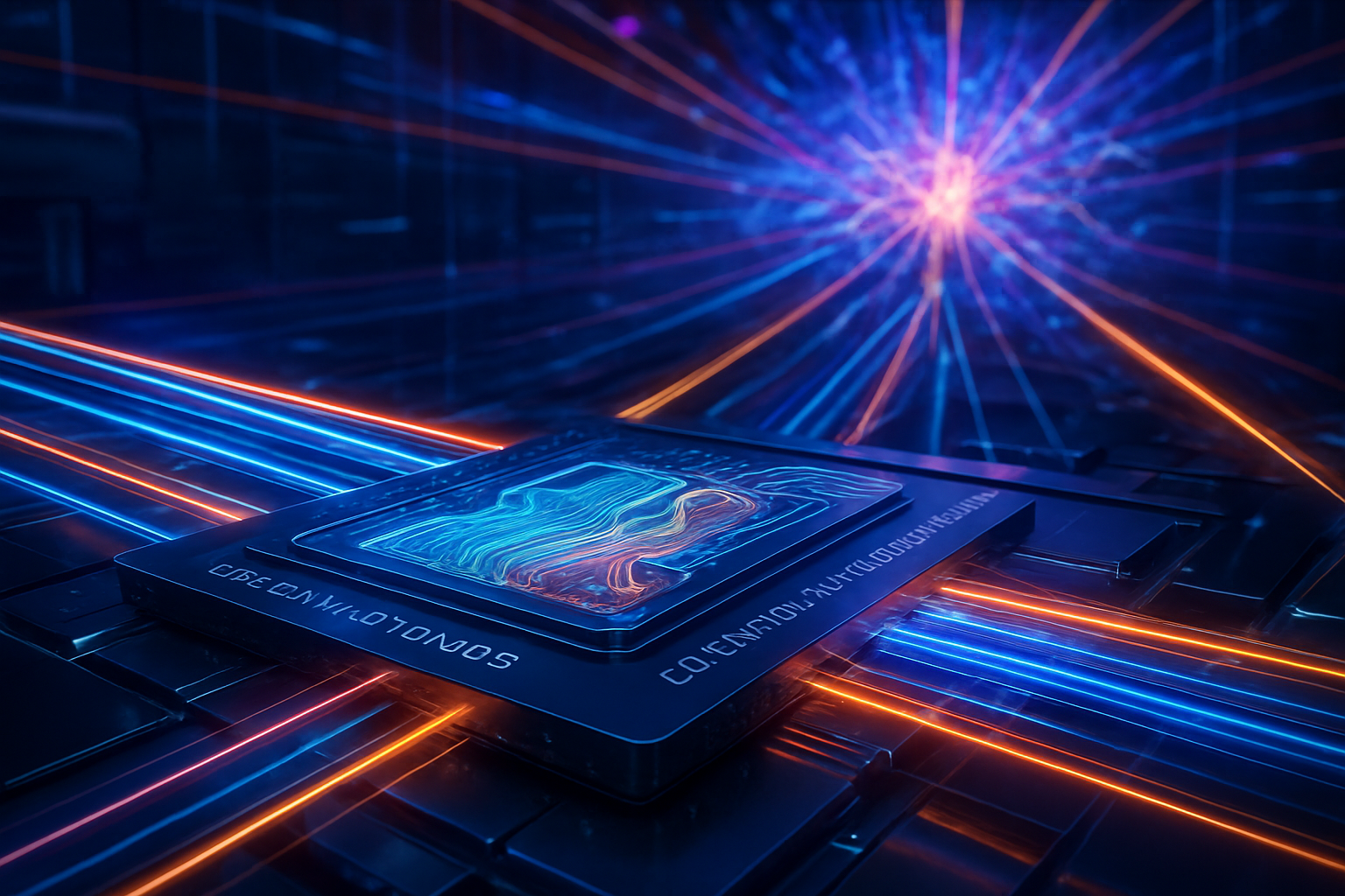
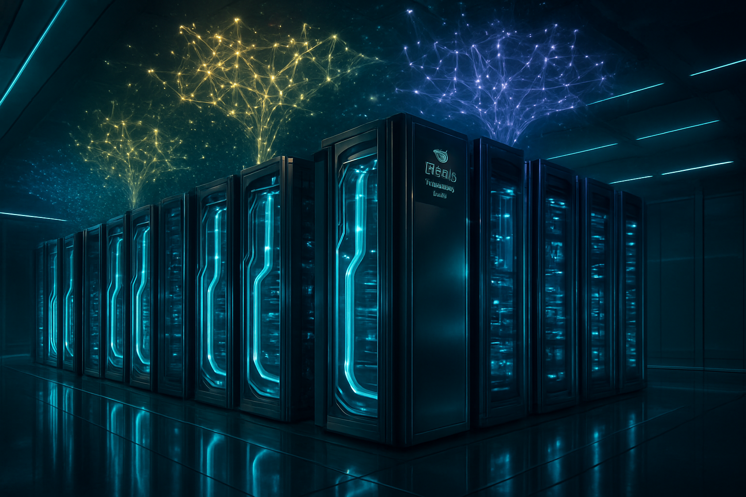
The Vera Rubin architecture represents a leap into the 3nm process node, allowing for a 1.6x increase in transistor density over the Blackwell generation. At the heart of the NVL72 rack is the Rubin GPU, which introduces the NVFP4 (4-bit floating point) precision format. This advancement allows the system to process data with significantly fewer bits without sacrificing accuracy, leading to a 5x performance uplift in inference tasks. The NVL72 configuration—a unified, liquid-cooled rack featuring 72 Rubin GPUs and 36 Vera CPUs—operates as a single, massive GPU, capable of processing the world's most complex Mixture-of-Experts (MoE) models with unprecedented fluidity.
The true "secret sauce" of the Rubin deployment, however, is the transition to HBM4 memory. With a staggering 22 TB/s of bandwidth per GPU, NVIDIA has effectively dismantled the "memory wall" that hampered previous architectures. This massive throughput is paired with the Vera CPU—a custom ARM-based processor featuring 88 "Olympus" cores—which shares a coherent memory pool with the GPU. This co-design ensures that data movement between the CPU and GPU is nearly instantaneous, a requirement for the low-latency reasoning required by next-generation AI agents.
Initial reactions from the AI research community have been overwhelmingly positive. Dr. Elena Rossi, a lead researcher at the European AI Initiative, noted that "the ability to train a 10-trillion parameter model with one-fourth the number of GPUs required just 18 months ago will democratize high-end AI research." Industry experts highlight the "blind-mate" liquid cooling system and cableless design of the NVL72 as a logistics breakthrough, claiming it reduces the installation and commissioning time of a new AI cluster from weeks to mere days.
The Hyperscaler Arms Race: Who Benefits from Rubin?
The deployment of Rubin NVL72 is already reshaping the power dynamics among tech giants. Microsoft (NASDAQ: MSFT) has emerged as the lead partner, integrating Rubin racks into its "Fairwater" AI super-factories. By being the first to market with Rubin-powered Azure instances, Microsoft aims to solidify its lead in the generative AI space, providing the necessary compute for OpenAI’s latest reasoning-heavy models. Similarly, Amazon (NASDAQ: AMZN) and Alphabet (NASDAQ: GOOGL) are racing to update their AWS and Google Cloud footprints, focusing on Rubin’s efficiency to lower the "token tax" for enterprise customers.
However, the Rubin launch also provides a strategic opening for specialized AI cloud providers like CoreWeave and Lambda. These companies have pivoted their entire business models around NVIDIA's "rack-scale" philosophy, offering early access to Rubin NVL72 to startups that are being priced out of the hyperscale giants. Meanwhile, the competitive landscape is heating up as AMD (NASDAQ: AMD) prepares its Instinct MI400 series. While AMD’s upcoming chip boasts a higher raw memory capacity of 432GB HBM4, NVIDIA’s vertical integration—combining networking, CPU, and GPU into a single software-defined rack—remains a formidable barrier to entry for its rivals.
For Meta (NASDAQ: META), the arrival of Rubin is a double-edged sword. While Mark Zuckerberg’s company remains one of NVIDIA's largest customers, it is simultaneously investing in its own MTIA chips and the UALink open standard to mitigate long-term reliance on a single vendor. The success of Rubin in early 2026 will determine whether Meta continues its massive NVIDIA spending spree or accelerates its transition to internal silicon for inference workloads.
The Global Context: Sovereign AI and the Energy Crisis
Beyond the corporate balance sheets, the Rubin deployment carries heavy geopolitical and environmental significance. The "Sovereign AI" movement has gained massive momentum, with European nations like France and Germany investing billions to build national AI factories using Rubin hardware. By hosting their own NVL72 clusters, these nations aim to ensure that sensitive state data and cultural intelligence remain on domestic soil, reducing their dependence on US-based cloud providers.
This massive expansion comes at a cost: energy. In 2026, the power consumption of AI data centers has become a top-tier political issue. While the Rubin architecture is significantly more efficient per watt, the sheer volume of GPUs being deployed is straining national grids. This has led to a radical shift in infrastructure, with Microsoft and Amazon increasingly investing in Small Modular Reactors (SMRs) and direct-to-chip liquid cooling to keep their 130kW Rubin racks operational without triggering regional blackouts.
Comparing this to previous milestones, the Rubin launch feels less like the release of a new chip and more like the rollout of a new utility. In the same way the electrical grid transformed the 20th century, the Rubin NVL72 is being viewed as the foundational infrastructure for a "reasoning economy." Concerns remain, however, regarding the concentration of this power in the hands of a few corporations, and whether the 25x cost reduction will be passed on to consumers or used to pad the margins of the silicon elite.
Future Horizons: From Generative to Agentic AI
Looking ahead to the remainder of 2026 and into 2027, the focus will likely shift from the raw training of models to "Physical AI" and autonomous robotics. Experts predict that the Rubin architecture’s efficiency will enable a new class of edge-capable models that can run on-premise in factories and hospitals. The next challenge for NVIDIA will be scaling this liquid-cooled architecture down to smaller footprints without losing the interconnect advantages of the NVLink 6 protocol.
Furthermore, as the industry moves toward 400 billion and 1 trillion parameter models as the standard, the pressure on memory bandwidth will only increase. We expect to see NVIDIA announce "Rubin Ultra" variations by late 2026, pushing HBM4 capacities even further. The long-term success of this architecture depends on how well the software ecosystem, particularly CUDA 13 and the new "Agentic SDKs," can leverage the massive hardware overhead now available in these data centers.
Conclusion: The Architecture of the Future
The deployment of NVIDIA's Vera Rubin NVL72 is a watershed moment for the technology industry. By delivering a 25x improvement in cost and energy efficiency for the most demanding AI tasks, NVIDIA has once again set the pace for the digital age. This hardware doesn't just represent faster compute; it represents the viability of AI as a sustainable, ubiquitous force in modern society.
As the first racks go live in the US and Europe, the tech world will be watching closely to see if the promised efficiency gains translate into lower costs for developers and more capable AI for consumers. In the coming weeks, keep an eye on the first performance benchmarks from the Microsoft Fairwater facility, as these will likely set the baseline for the "reasoning era" of 2026.
This content is intended for informational purposes only and represents analysis of current AI developments.
TokenRing AI delivers enterprise-grade solutions for multi-agent AI workflow orchestration, AI-powered development tools, and seamless remote collaboration platforms.
For more information, visit https://www.tokenring.ai/.