Tag: Data Centers

  • The Era of Light: Photonic Interconnects Shatter the ‘Copper Wall’ in AI Scaling

    The Era of Light: Photonic Interconnects Shatter the ‘Copper Wall’ in AI Scaling

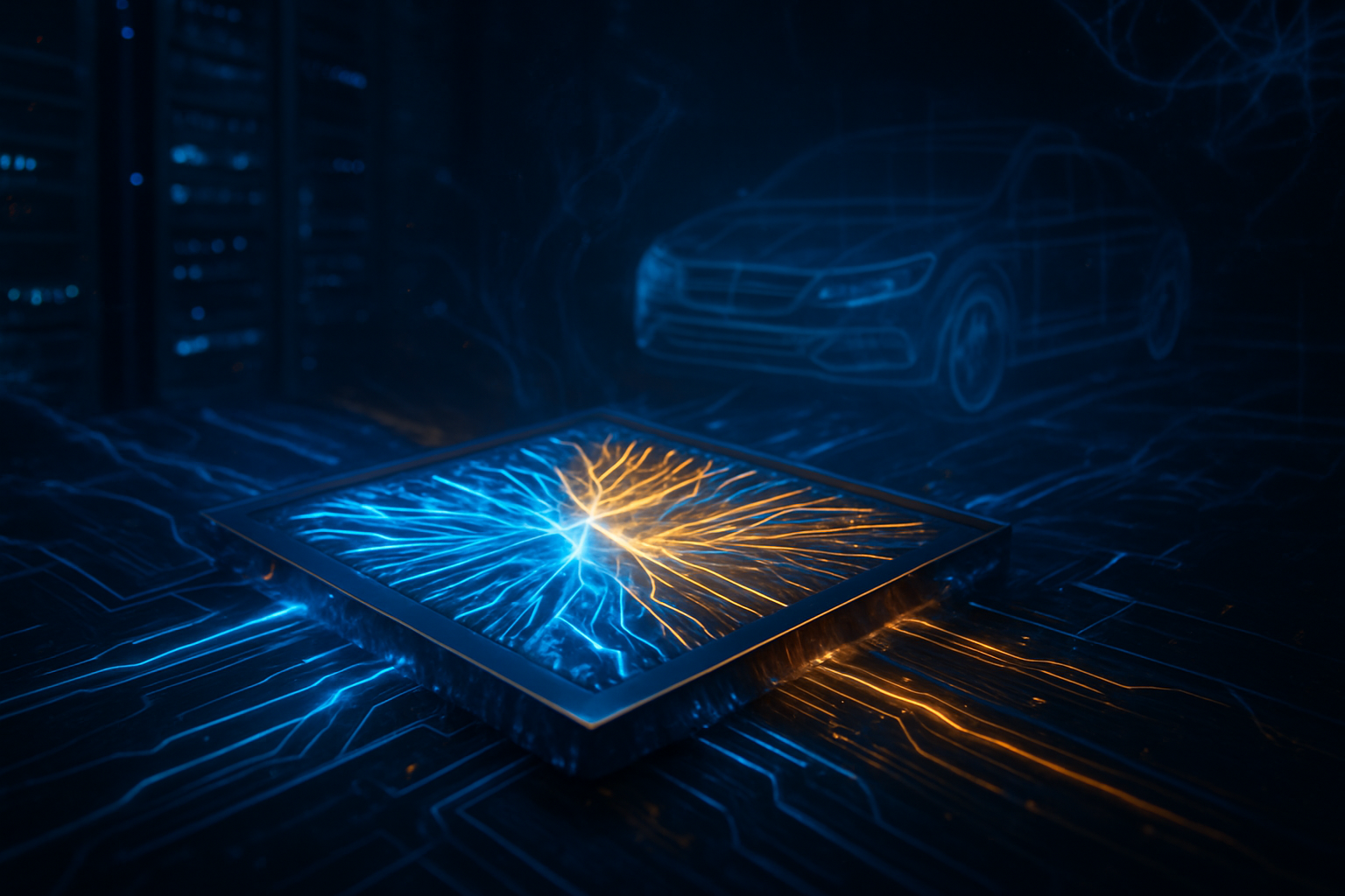
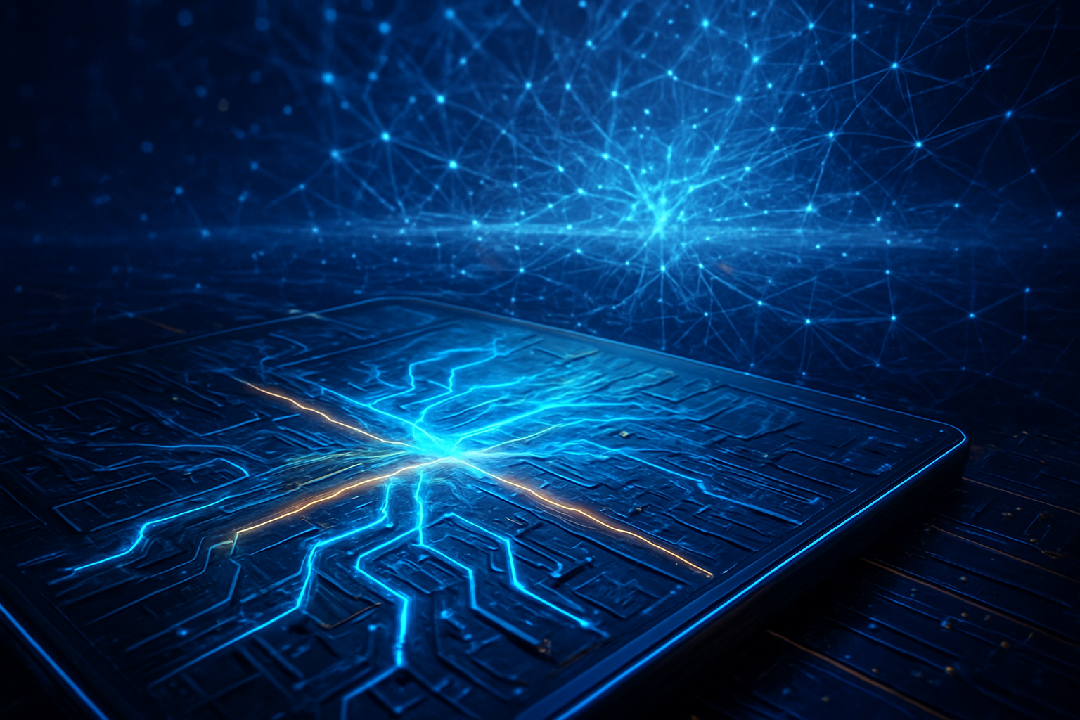
    As of January 9, 2026, the artificial intelligence industry has officially reached a historic architectural milestone: the transition from electricity to light as the primary medium for data movement. For decades, copper wiring has been the backbone of computing, but the relentless demands of trillion-parameter AI models have finally pushed electrical signaling to its physical breaking point. This phenomenon, known as the "Copper Wall," threatened to stall the growth of AI clusters just as the world moved toward the million-GPU era.

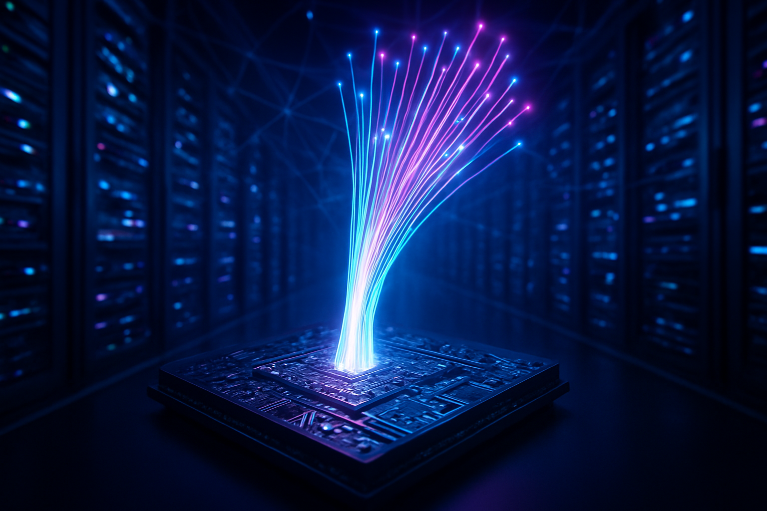
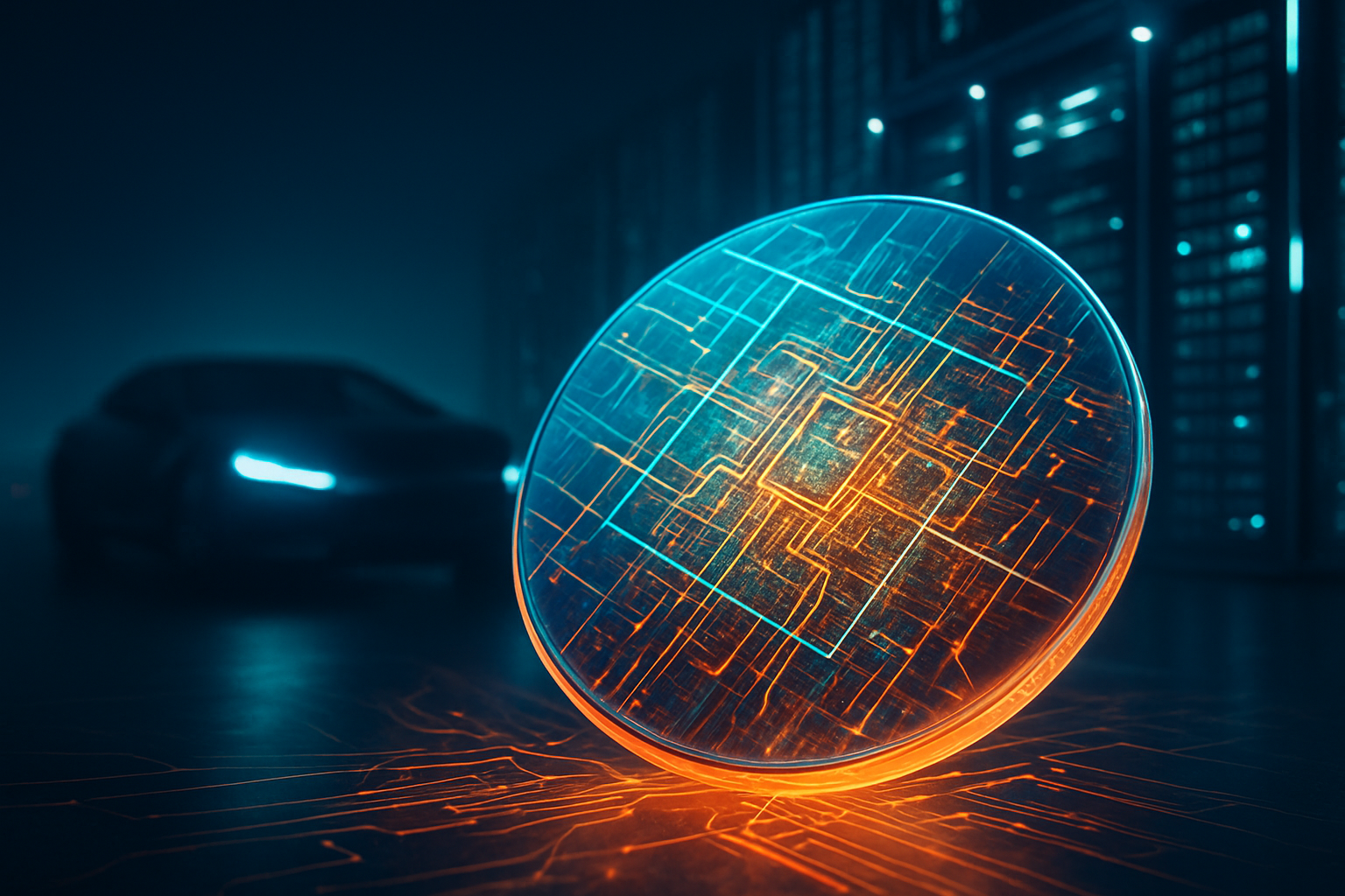
    The solution, now being deployed in high-volume production across the globe, is Photonic Interconnects. By integrating Optical I/O (Input/Output) directly into the silicon package, companies are replacing traditional electrical pins with microscopic lasers and light-modulating chiplets. This shift is not merely an incremental upgrade; it represents a fundamental decoupling of compute performance from the energy and distance constraints of electricity, enabling a 70% reduction in interconnect power and a 10x increase in bandwidth density.

    Breaking the I/O Tax: The Technical Leap to 5 pJ/bit

    The technical crisis that precipitated this revolution was the "I/O Tax"—the massive amount of energy required simply to move data between GPUs. In legacy 2024-era clusters, moving data across a rack could consume up to 30% of a system's total power budget. At the new 224 Gbps and 448 Gbps per-lane data rates required for 2026 workloads, copper signals degrade after traveling just a few inches. Optical I/O solves this by converting electrons to photons at the "shoreline" of the chip. This allows data to travel hundreds of meters with virtually no signal loss and minimal heat generation.

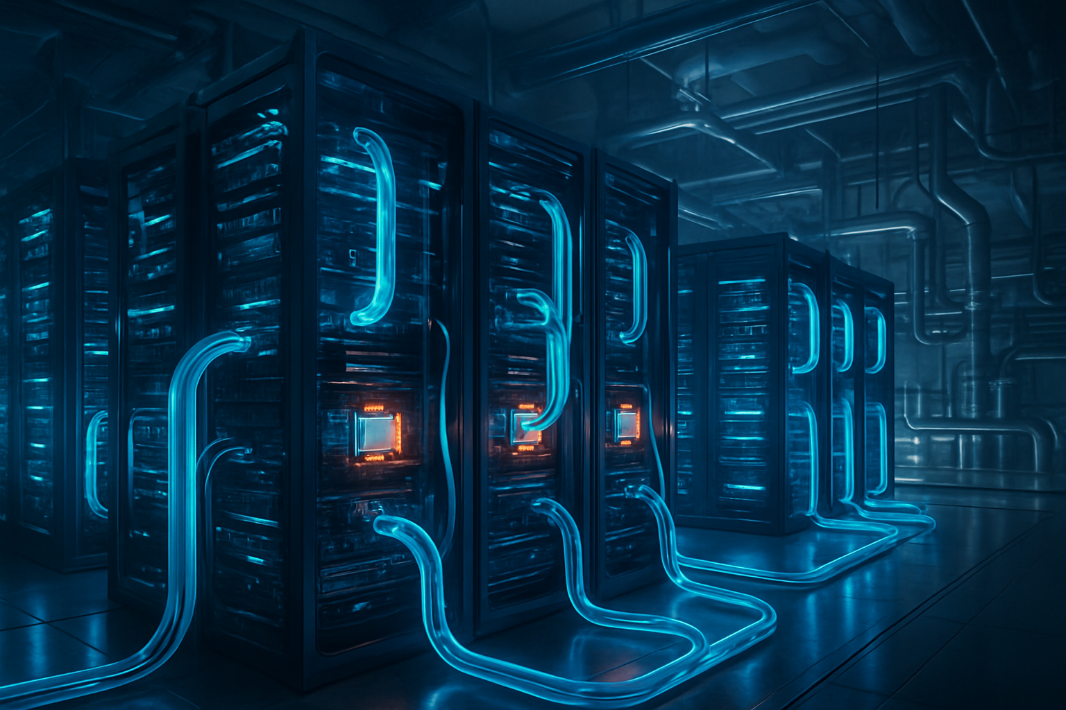
    Leading the charge in technical specifications is Lightmatter, whose Passage M1000 platform has become a cornerstone of the 2026 AI data center. Unlike previous Co-Packaged Optics (CPO) that placed optical engines at the edge of a chip, Lightmatter’s 3D photonic interposer allows GPUs to sit directly on top of a photonic layer. This enables a record-breaking 114 Tbps of aggregate bandwidth and a bandwidth density of 1.4 Tbps/mm². Meanwhile, Ayar Labs has moved into high-volume production of its TeraPHY Gen 3 chiplets, which are the first to carry Universal Chiplet Interconnect Express (UCIe) traffic optically, achieving power efficiencies as low as 5 picojoules per bit (pJ/bit).

    This new approach differs fundamentally from the "pluggable" transceivers of the past. In previous generations, optical modules were bulky components plugged into the front of a switch. In the 2026 paradigm, the laser source is often external for serviceability (standardized as ELSFP), but the modulation and detection happen inside the GPU or Switch package itself. This "Direct Drive" architecture eliminates the need for power-hungry Digital Signal Processors (DSPs), which were a primary source of latency and heat in earlier optical attempts.

    The New Power Players: NVIDIA, Broadcom, and the Marvell-Celestial Merger

    The shift to photonics has redrawn the competitive map of the semiconductor industry. NVIDIA (NASDAQ: NVDA) signaled its dominance in this new era at CES 2026 with the official launch of the Rubin platform. Rubin makes optical I/O a core requirement, utilizing Spectrum-X Ethernet Photonics and Quantum-X800 InfiniBand switches. By integrating silicon photonic engines developed with TSMC (NYSE: TSM) directly into the switch ASIC, NVIDIA has achieved a 5x power reduction per 1.6 Tb/s port, ensuring their "single-brain" cluster architecture can scale to millions of interconnected nodes.

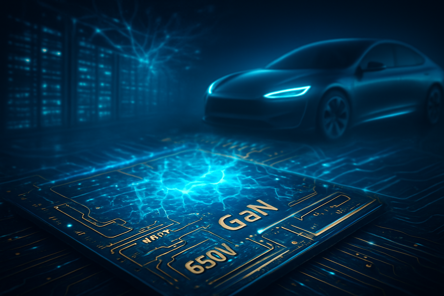
    Broadcom (NASDAQ: AVGO) has also secured a massive lead with its Tomahawk 6 (Davisson) switch, which began volume shipping in late 2025. The TH6-Davisson is a behemoth, boasting 102.4 Tbps of total switching capacity. By utilizing integrated 6.4 Tbps optical engines, Broadcom has effectively cornered the market for hyperscale Ethernet backbones. Not to be outdone, Marvell (NASDAQ: MRVL) made a seismic move in early January 2026 by announcing the $3.25 billion acquisition of Celestial AI. This merger combines Marvell’s robust CXL and PCIe switching portfolio with Celestial’s "Photonic Fabric," a technology specifically designed for optical memory pooling, allowing GPUs to share HBM4 memory across a rack at light speed.

    For startups and smaller AI labs, this development is a double-edged sword. While photonic interconnects lower the long-term operational costs of AI clusters by slashing energy bills, the capital expenditure required to build light-based infrastructure is significantly higher. This reinforces the strategic advantage of "Big Tech" hyperscalers like Amazon (NASDAQ: AMZN) and Google (NASDAQ: GOOGL), who have the capital to transition their entire fleets to photonic-ready architectures.

    A Paradigm Shift: From Moore’s Law to the Million-GPU Cluster

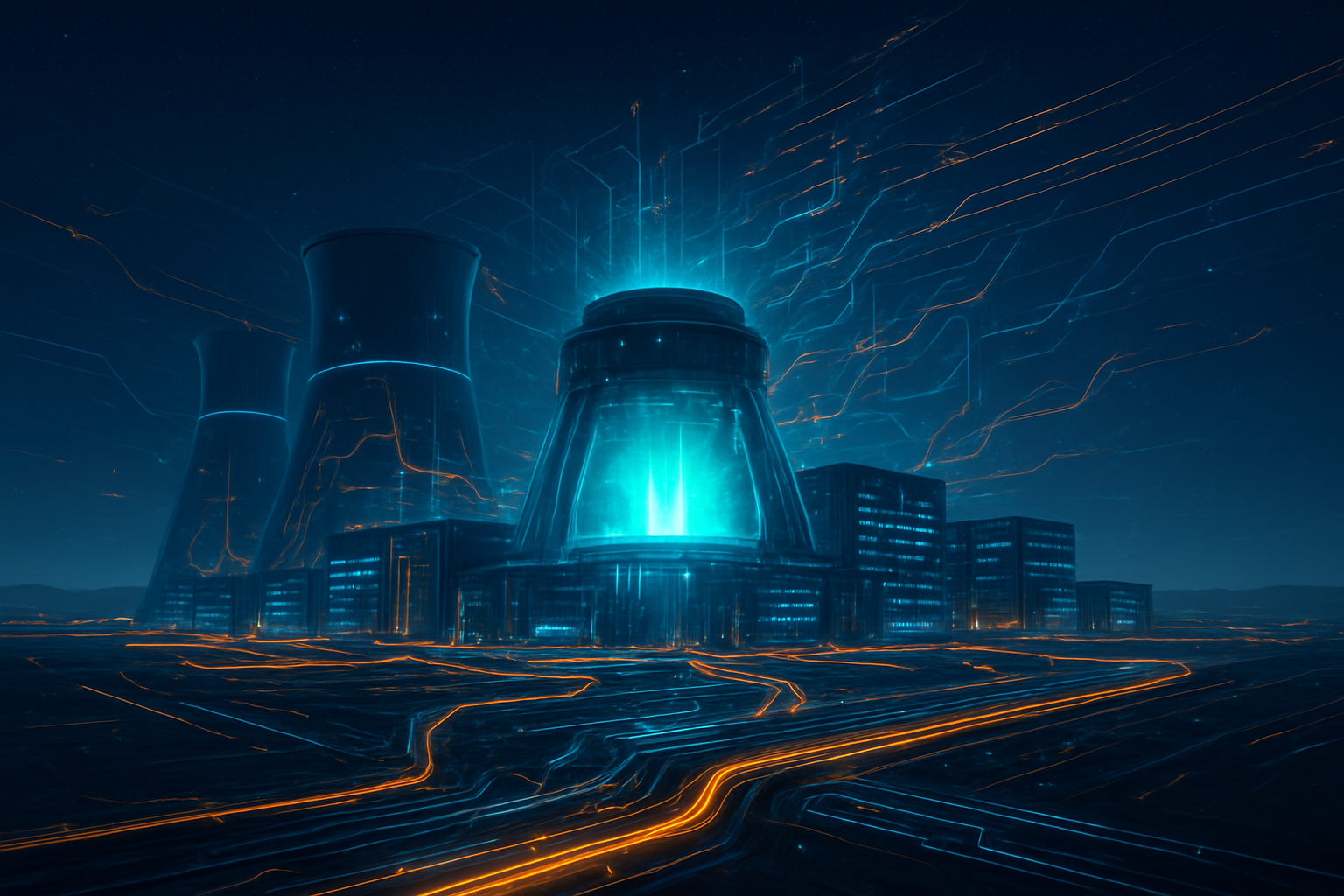
    The wider significance of photonic interconnects cannot be overstated. For years, industry observers feared that Moore’s Law was reaching a hard limit—not because we couldn't make smaller transistors, but because we couldn't get data to those transistors fast enough without melting the chip. The "interconnect bottleneck" was the single greatest threat to the continued scaling of Large Language Models (LLMs) and World Models. By moving to light, the industry has bypassed this physical wall, effectively extending the roadmap for AI scaling for another decade.

    This transition also addresses the growing global concern over the energy consumption of AI data centers. By reducing the power required for data movement by 70%, photonics provides a much-needed "green" dividend. However, this breakthrough also brings new concerns, particularly regarding the complexity of the supply chain. The manufacturing of silicon photonics requires specialized cleanrooms and high-precision packaging techniques that are currently concentrated in a few locations, such as TSMC’s advanced packaging facilities in Taiwan.

    Comparatively, the move to Optical I/O is being viewed as a milestone on par with the introduction of the GPU itself. If the GPU gave AI its "brain," photonic interconnects are giving it a "nervous system" capable of near-instantaneous communication across vast distances. This enables the transition from isolated servers to "warehouse-scale computers," where the entire data center functions as a single, coherent processing unit.

    The Road to 2027: All-Optical Computing and Beyond

    Looking ahead, the near-term focus will be on the refinement of Co-Packaged Optics and the stabilization of external laser sources. Experts predict that by 2027, we will see the first "all-optical" switch fabrics where data is never converted back into electrons between the source and the destination. This would further reduce latency to the absolute limits of the speed of light, enabling real-time training of models that are orders of magnitude larger than GPT-5.

    Potential applications on the horizon include "Disaggregated Memory," where banks of high-speed memory can be located in a separate part of the data center from the processors, connected via optical fabric. This would allow for much more flexible and efficient use of expensive hardware resources. Challenges remain, particularly in the yield rates of integrated photonic chiplets and the long-term reliability of microscopic lasers, but the industry's massive R&D investment suggests these are hurdles, not roadblocks.

    Summary: A New Foundation for Intelligence

    The revolution in photonic interconnects marks the end of the "Copper Age" of high-performance computing. Key takeaways from this transition include the massive 70% reduction in I/O power, the rise of 100+ Tbps switching capacities, and the dominance of integrated silicon photonics in the roadmaps of industry leaders like NVIDIA, Broadcom, and Intel (NASDAQ: INTC).

    This development will likely be remembered as the moment when AI scaling became decoupled from the physical constraints of electricity. In the coming months, watch for the first performance benchmarks from NVIDIA’s Rubin clusters and the finalized integration of Celestial AI’s fabric into Marvell’s silicon. The "Era of Light" is no longer a futuristic concept; it is the current reality of the global AI infrastructure.


    This content is intended for informational purposes only and represents analysis of current AI developments.

    TokenRing AI delivers enterprise-grade solutions for multi-agent AI workflow orchestration, AI-powered development tools, and seamless remote collaboration platforms.
    For more information, visit https://www.tokenring.ai/.

  • Shattering the Silicon Ceiling: Tower Semiconductor and LightIC Unveil Photonics Breakthrough to Power the Next Decade of AI and Autonomy

    Shattering the Silicon Ceiling: Tower Semiconductor and LightIC Unveil Photonics Breakthrough to Power the Next Decade of AI and Autonomy

    In a landmark announcement that signals a paradigm shift for both artificial intelligence infrastructure and autonomous mobility, Tower Semiconductor (NASDAQ: TSEM) and LightIC Technologies have unveiled a strategic partnership to mass-produce the world’s first monolithic 4D FMCW LiDAR and high-bandwidth optical interconnect chips. Announced on January 5, 2026, just days ahead of the Consumer Electronics Show (CES), this collaboration leverages Tower’s advanced 300mm silicon photonics (SiPho) foundry platform to integrate entire "optical benches"—lasers, modulators, and detectors—directly onto a single silicon substrate.

    The immediate significance of this development cannot be overstated. By successfully transitioning silicon photonics from experimental lab settings to high-volume manufacturing, the partnership addresses the two most critical bottlenecks in modern technology: the "memory wall" that limits AI model scaling in data centers and the high cost and unreliability of traditional sensing for autonomous vehicles. This breakthrough promises to slash power consumption in AI factories while providing self-driving systems with the "velocity awareness" required for safe urban navigation, effectively bridging the gap between digital and physical AI.

    The Technical Leap: 4D FMCW and the End of the Copper Era

    At the heart of the Tower-LightIC partnership is the commercialization of Frequency-Modulated Continuous-Wave (FMCW) LiDAR, a technology that differs fundamentally from the Time-of-Flight (ToF) systems currently used by most automotive manufacturers. While ToF LiDAR pulses light to measure distance, the new LightIC "Lark" and "FR60" chips utilize a continuous wave of light to measure both distance and instantaneous velocity—the fourth dimension—simultaneously for every pixel. This coherent detection method ensures that the sensors are immune to interference from sunlight or other LiDAR systems, a persistent challenge for existing technologies.

    Technically, the integration is achieved using Tower Semiconductor's PH18 process, which allows for the monolithic integration of III-V lasers with silicon-based optical components. The resulting "Lark" automotive chip boasts a detection range of up to 500 meters with a velocity precision of 0.05 meters per second. This level of precision allows a vehicle's AI to instantly distinguish between a stationary object and a pedestrian stepping into a lane, significantly reducing the "perception latency" that currently plagues autonomous driving stacks.

    Furthermore, the same silicon photonics platform is being applied to solve the data bottleneck within AI data centers. As AI models grow in complexity, the traditional copper interconnects used to move data between GPUs and High Bandwidth Memory (HBM) have become a liability, consuming excessive power and generating heat. The new optical interconnect chips enable multi-wavelength laser sources that provide bandwidth of up to 3.2 Tbps. By moving data via light rather than electricity, these chips reduce interconnect latency to a staggering 5 nanoseconds per meter, compared to the 15-20 picajoules per bit required by standard pluggable optics.

    Initial reactions from the AI research community have been overwhelmingly positive. Dr. Elena Vance, a senior researcher in photonics, noted that "the ability to manufacture these components on standard 300mm wafers at Tower's scale is the 'holy grail' of the industry. We are finally moving away from discrete, bulky optical components toward a truly integrated, solid-state future."

    Market Disruption: A New Hierarchy in AI Infrastructure

    The strategic alliance between Tower Semiconductor and LightIC creates immediate competitive pressure for industry giants like Nvidia (NASDAQ: NVDA), Marvell Technology (NASDAQ: MRVL), and Broadcom (NASDAQ: AVGO). While these companies have dominated the AI hardware space, the shift toward Co-Packaged Optics (CPO) and integrated silicon photonics threatens to disrupt established supply chains. Companies that can integrate photonics directly into their chipsets will hold a significant advantage in power efficiency and compute density.

    For data center operators like Amazon (NASDAQ: AMZN), Google (NASDAQ: GOOGL), and Meta (NASDAQ: META), this breakthrough offers a path toward "Green AI." As energy consumption in AI factories becomes a regulatory and financial hurdle, the transition to optical interconnects allows these giants to scale their clusters without hitting a thermal ceiling. The lower power profile of the Tower-LightIC chips could potentially reduce the total cost of ownership (TCO) for massive AI clusters by as much as 30% over a five-year period.

    In the automotive sector, the availability of low-cost, high-performance 4D LiDAR could democratize Level 4 and Level 5 autonomy. Currently, high-end LiDAR systems can cost thousands of dollars per unit, limiting them to luxury vehicles or experimental fleets. LightIC’s FR60 chip, designed for compact robotics and mass-market vehicles, aims to bring this cost down to a point where it can be standard equipment in entry-level consumer cars. This puts pressure on traditional sensor companies and may force a consolidation in the LiDAR market as solid-state silicon photonics becomes the dominant architecture.

    The Broader Significance: Toward "Physical AI" and Sustainability

    The convergence of sensing and communication on a single silicon platform marks a major milestone in the evolution of "Physical AI"—the application of artificial intelligence to the physical world through robotics and autonomous systems. By providing robots and vehicles with human-like (or better-than-human) perception at a fraction of the current energy cost, this breakthrough accelerates the timeline for truly autonomous logistics and urban mobility.

    This development also fits into the broader trend of "Compute-as-a-Light-Source." For years, the industry has warned of the "End of Moore’s Law" due to the physical limitations of shrinking transistors. Silicon photonics bypasses many of these limits by using photons instead of electrons for data movement. This is not just an incremental improvement; it is a fundamental shift in how information is processed and transported.

    However, the transition is not without its challenges. The shift to silicon photonics requires a complete overhaul of packaging and testing infrastructures. There are also concerns regarding the geopolitical nature of semiconductor manufacturing. As Tower Semiconductor expands its 300mm capacity, the strategic importance of foundry locations and supply chain resilience becomes even more pronounced. Nevertheless, the environmental impact of this technology—reducing the massive carbon footprint of AI training—is a significant positive that aligns with global sustainability goals.

    The Horizon: 1.6T Interconnects and Consumer-Grade Robotics

    Looking ahead, experts predict that the Tower-LightIC partnership is just the first wave of a photonics revolution. In the near term, we expect to see the release of 1.6T and 3.2T second-generation interconnects that will become the backbone of "GPT-6" class model training. These will likely be integrated into the next generation of AI supercomputers, enabling nearly instantaneous data sharing across thousands of nodes.

    In the long term, the "FR60" compact LiDAR chip is expected to find its way into consumer electronics beyond the automotive sector. Potential applications include high-precision spatial computing for AR/VR headsets and sophisticated obstacle avoidance for consumer-grade drones and home service robots. The challenge will be maintaining high yields during the mass-production phase, but Tower’s proven track record in analog and mixed-signal manufacturing provides a strong foundation for success.

    Industry analysts predict that by 2028, silicon photonics will account for over 40% of the total data center interconnect market. "The era of the electron is giving way to the era of the photon," says market analyst Marcus Thorne. "What we are seeing today is the foundation for the next twenty years of computing."

    A New Chapter in Semiconductor History

    The partnership between Tower Semiconductor and LightIC Technologies represents a definitive moment in the history of semiconductors. By solving the data bottleneck in AI data centers and providing a high-performance, low-cost solution for autonomous sensing, these two companies have cleared the path for the next generation of AI-driven innovation.

    The key takeaway for the industry is that the integration of optical and electrical components is no longer a futuristic concept—it is a manufacturing reality. As these chips move into mass production throughout 2026, the tech world will be watching closely to see how quickly they are adopted by the major cloud providers and automotive OEMs. This development is not just about faster chips or better sensors; it is about enabling a future where AI can operate seamlessly and sustainably in both the digital and physical realms.

    In the coming months, keep a close eye on the initial deployment of "Lark" B-samples in automotive pilot programs and the first integration of Tower’s 3.2T optical engines in commercial AI clusters. The light-speed revolution has officially begun.


    This content is intended for informational purposes only and represents analysis of current AI developments.

    TokenRing AI delivers enterprise-grade solutions for multi-agent AI workflow orchestration, AI-powered development tools, and seamless remote collaboration platforms.
    For more information, visit https://www.tokenring.ai/.

  • Breaking the Copper Wall: Co-Packaged Optics and Silicon Photonics Usher in the Million-GPU Era

    Breaking the Copper Wall: Co-Packaged Optics and Silicon Photonics Usher in the Million-GPU Era

    As of January 8, 2026, the artificial intelligence industry has officially collided with a physical limit known as the "Copper Wall." At data transfer speeds of 224 Gbps and beyond, traditional copper wiring can no longer carry signals more than a few inches without massive signal degradation and unsustainable power consumption. To circumvent this, the world’s leading semiconductor and networking firms have pivoted to Co-Packaged Optics (CPO) and Silicon Photonics, a paradigm shift that integrates fiber-optic communication directly into the chip package. This breakthrough is not just an incremental upgrade; it is the foundational technology enabling the first million-GPU clusters and the training of trillion-parameter AI models.

    The immediate significance of this transition is staggering. By moving the conversion of electrical signals to light (photonics) from separate pluggable modules directly onto the processor or switch substrate, companies are slashing energy consumption by up to 70%. In an era where data center power demands are straining national grids, the ability to move data at 102.4 Tbps while significantly reducing the "tax" of data movement has become the most critical metric in the AI arms race.

    The technical specifications of the current 2026 hardware generation highlight a massive leap over the pluggable optics of 2024. Broadcom Inc. (NASDAQ: AVGO) has begun volume shipping its "Davisson" Tomahawk 6 switch, the industry’s first 102.4 Tbps Ethernet switch. This device utilizes 16 integrated 6.4 Tbps optical engines, leveraging TSMC’s Compact Universal Photonic Engine (COUPE) technology. Unlike previous generations that relied on power-hungry Digital Signal Processors (DSPs) to push signals through copper traces, CPO systems like Davisson use "Direct Drive" architectures. This eliminates the DSP entirely for short-reach links, bringing energy efficiency down from 15–20 picojoules per bit (pJ/bit) to a mere 5 pJ/bit.

    NVIDIA (NASDAQ: NVDA) has similarly embraced this shift with its Quantum-X800 InfiniBand platform. By utilizing micro-ring modulators, NVIDIA has achieved a bandwidth density of over 1.0 Tbps per millimeter of chip "shoreline"—a five-fold increase over traditional methods. This density is crucial because the physical perimeter of a chip is limited; silicon photonics allows dozens of data channels to be multiplexed onto a single fiber using Wavelength Division Multiplexing (WDM), effectively bypassing the physical constraints of electrical pins.

    The research community has hailed these developments as the "end of the pluggable era." Early reactions from the Open Compute Project (OCP) suggest that the shift to CPO has solved the "Distance-Speed Tradeoff." Previously, high-speed signals were restricted to distances of less than one meter. With silicon photonics, these same signals can now travel up to 2 kilometers with negligible latency (5–10ns compared to the 100ns+ required by DSP-based systems), allowing for "disaggregated" data centers where compute and memory can be located in different racks while behaving as a single monolithic machine.

    The commercial landscape for AI infrastructure is being radically reshaped by this optical transition. Broadcom and NVIDIA have emerged as the primary beneficiaries, having successfully integrated photonics into their core roadmaps. NVIDIA’s latest "Rubin" R100 platform, which entered production in late 2025, makes CPO mandatory for its rack-scale architecture. This move forces competitors to either develop similar in-house photonic capabilities or rely on third-party chiplet providers like Ayar Labs, which recently reached high-volume production of its TeraPHY optical I/O chiplets.

    Intel Corporation (NASDAQ: INTC) has also pivoted its strategy, having divested its traditional pluggable module business to Jabil in late 2024 to focus exclusively on high-value Optical Compute Interconnect (OCI) chiplets. Intel’s OCI is now being sampled by major cloud providers, offering a standardized way to add optical I/O to custom AI accelerators. Meanwhile, Marvell Technology (NASDAQ: MRVL) is positioning itself as the leader in the "Scale-Up" market, using its acquisition of Celestial AI’s photonic fabric to power the next generation of UALink-compatible switches, which are expected to sample in the second half of 2026.

    This shift creates a significant barrier to entry for smaller AI chip startups. The complexity of 2.5D and 3D packaging required to co-package optics with silicon is immense, requiring deep partnerships with foundries like TSMC and specialized OSAT (Outsourced Semiconductor Assembly and Test) providers. Major AI labs, such as OpenAI and Anthropic, are now factoring "optical readiness" into their long-term compute contracts, favoring providers who can offer the lower TCO (Total Cost of Ownership) and higher reliability that CPO provides.

    The wider significance of Co-Packaged Optics lies in its impact on the "Power Wall." A cluster of 100,000 GPUs using traditional interconnects can consume over 60 Megawatts just for data movement. By switching to CPO, data center operators can reclaim that power for actual computation, effectively increasing the "AI work per watt" by a factor of three. This is a critical development for global sustainability goals, as the energy footprint of AI has become a point of intense regulatory scrutiny in early 2026.

    Furthermore, CPO addresses the long-standing issue of reliability in large-scale systems. In the past, the laser—the most failure-prone component of an optical link—was embedded deep inside the chip package, making a single laser failure a catastrophic event for a $40,000 GPU. The 2026 generation of hardware has standardized the External Laser Source (ELSFP), a field-replaceable unit that keeps the heat-generating laser away from the compute silicon. This "pluggable laser" approach combines the reliability of traditional optics with the performance of co-packaging.

    Comparisons are already being drawn to the introduction of High Bandwidth Memory (HBM) in 2015. Just as HBM solved the "Memory Wall" by moving memory closer to the processor, CPO is solving the "Interconnect Wall" by moving the network into the package. This evolution suggests that the future of AI scaling is no longer about making individual chips faster, but about making the entire data center act as a single, fluid fabric of light.

    Looking ahead, the next 24 months will likely see the integration of silicon photonics directly with HBM4. This would allow for "Optical CXL," where a GPU could access memory located hundreds of meters away with the same latency as local on-board memory. Experts predict that by 2027, we will see the first all-optical backplanes, eliminating copper from the data center fabric entirely.

    However, challenges remain. The industry is still debating the standardization of optical interfaces. While the Ultra Accelerator Link (UALink) consortium has made strides, a "standards war" between InfiniBand-centric and Ethernet-centric optical implementations continues. Additionally, the yield rates for 3D-stacked silicon photonics remain lower than traditional CMOS, though they are improving as TSMC and Intel refine their specialized photonic processes.

    The most anticipated development for late 2026 is the deployment of 1.6T and 3.2T optical links per lane. As AI models move toward "World Models" and multi-modal reasoning that requires massive real-time data ingestion, these speeds will transition from a luxury to a necessity. Experts predict that the first "Exascale AI" system, capable of a quintillion operations per second, will be built entirely on a silicon photonics foundation.

    The transition to Co-Packaged Optics and Silicon Photonics represents a watershed moment in the history of computing. By breaking the "Copper Wall," the industry has ensured that the scaling laws of AI can continue for at least another decade. The move from 20 pJ/bit to 5 pJ/bit is not just a technical win; it is an economic and environmental necessity that enables the massive infrastructure projects currently being planned by the world's largest technology companies.

    As we move through 2026, the key metrics to watch will be the volume ramp-up of Broadcom’s Tomahawk 6 and the field performance of NVIDIA’s Rubin platform. If these systems deliver on their promise of 70% power reduction and 10x bandwidth density, the "Optical Era" will be firmly established as the backbone of the AI revolution. The light-speed data center is no longer a laboratory dream; it is the reality of the 2026 AI landscape.


    This content is intended for informational purposes only and represents analysis of current AI developments.

    TokenRing AI delivers enterprise-grade solutions for multi-agent AI workflow orchestration, AI-powered development tools, and seamless remote collaboration platforms.
    For more information, visit https://www.tokenring.ai/.

  • The Power Revolution: Onsemi and GlobalFoundries Join Forces to Fuel the AI and EV Era with 650V GaN

    The Power Revolution: Onsemi and GlobalFoundries Join Forces to Fuel the AI and EV Era with 650V GaN

    In a move that signals a tectonic shift in the semiconductor landscape, power electronics giant onsemi (NASDAQ: ON) and contract manufacturing leader GlobalFoundries (NASDAQ: GFS) have announced a strategic partnership to develop and mass-produce 650V Gallium Nitride (GaN) power devices. Announced in late December 2025, this collaboration is designed to tackle the two most pressing energy challenges of 2026: the insatiable power demands of AI-driven data centers and the need for higher efficiency in the rapidly maturing electric vehicle (EV) market.

    The partnership represents a significant leap forward for wide-bandgap (WBG) materials, which are quickly replacing traditional silicon in high-performance applications. By combining onsemi's deep expertise in power systems and packaging with GlobalFoundries’ high-volume, U.S.-based manufacturing capabilities, the two companies aim to provide a resilient and scalable supply of GaN chips. As of January 7, 2026, the industry is already seeing the first ripples of this announcement, with customer sampling scheduled to begin in the first half of this year.

    The technical core of this partnership centers on a 200mm (8-inch) enhancement-mode (eMode) GaN-on-silicon manufacturing process. Historically, GaN production was limited to 150mm wafers, which constrained volume and kept costs high. The transition to 200mm wafers at GlobalFoundries' Malta, New York, facility allows for significantly higher yields and better cost-efficiency, effectively moving GaN from a niche, premium material to a mainstream industrial standard. The 650V rating is particularly strategic, as it serves as the "sweet spot" for devices that interface with standard electrical grids and the 400V battery architectures currently dominant in the automotive sector.

    Unlike traditional silicon transistors, which struggle with heat and efficiency at high frequencies, these 650V GaN devices can switch at much higher speeds with minimal energy loss. This capability allows engineers to use smaller passive components, such as inductors and capacitors, leading to a dramatic reduction in the overall size and weight of power supplies. Furthermore, onsemi is integrating these GaN FETs with its proprietary silicon drivers and controllers in a "system-in-package" (SiP) architecture. This integration reduces electromagnetic interference (EMI) and simplifies the design process for engineers, who previously had to manually tune discrete components from multiple vendors.

    Initial reactions from the semiconductor research community have been overwhelmingly positive. Analysts note that while Silicon Carbide (SiC) has dominated the high-voltage (1200V+) EV traction inverter market, GaN is proving to be the superior choice for the 650V range. Dr. Aris Silvestros, a leading power electronics researcher, commented that the "integration of gate drivers directly with GaN transistors on a 200mm line is the 'holy grail' for power density, finally breaking the thermal barriers that have plagued high-performance computing for years."

    For the broader tech industry, the implications are profound. AI giants and data center operators stand to be the biggest beneficiaries. As Large Language Models (LLMs) continue to scale, the power density of server racks has become a critical bottleneck. Traditional silicon-based power units are no longer sufficient to feed the latest AI accelerators. The onsemi-GlobalFoundries partnership enables the creation of 12kW power modules that fit into the same physical footprint as older 3kW units. This effectively quadruples the power density of data centers, allowing companies like NVIDIA (NASDAQ: NVDA) and Microsoft (NASDAQ: MSFT) to pack more compute power into existing facilities without requiring massive infrastructure overhauls.

    In the automotive sector, the partnership puts pressure on established players like Wolfspeed (NYSE: WOLF) and STMicroelectronics (NYSE: STM). While these competitors have focused heavily on Silicon Carbide, the onsemi-GF alliance's focus on 650V GaN targets the high-volume "onboard charger" (OBC) and DC-DC converter markets. By making these components smaller and more efficient, automakers can reduce vehicle weight and extend range—or conversely, use smaller, cheaper batteries to achieve the same range. The bidirectional capability of these GaN devices also facilitates "Vehicle-to-Grid" (V2G) technology, allowing EVs to act as mobile batteries for the home or the electrical grid, a feature that is becoming a standard requirement in 2026 model-year vehicles.

    Strategically, the partnership provides a major "Made in America" advantage. By utilizing GlobalFoundries' New York fabrication plants, onsemi can offer its customers a supply chain that is insulated from geopolitical tensions in East Asia. This is a critical selling point for U.S. and European automakers and government-linked data center projects that are increasingly prioritized by domestic content requirements and supply chain security.

    The broader significance of this development lies in the global "AI Power Crisis." As of early 2026, data centers are projected to consume over 1,000 Terawatt-hours of electricity annually. The efficiency gains offered by GaN—reducing heat loss by up to 50% compared to silicon—are no longer just a cost-saving measure; they are a prerequisite for the continued growth of artificial intelligence. If the world is to meet its sustainability goals while expanding AI capabilities, the transition to wide-bandgap materials like GaN is non-negotiable.

    This milestone also marks the end of the "Silicon Era" for high-performance power conversion. Much like the transition from vacuum tubes to transistors in the mid-20th century, the shift from Silicon to GaN and SiC represents a fundamental change in how we manage electrons. The partnership between onsemi and GlobalFoundries is a signal that the manufacturing hurdles that once held GaN back have been cleared. This mirrors previous AI milestones, such as the shift to GPU-accelerated computing; it is an enabling technology that allows the software and AI models to reach their full potential.

    However, the rapid transition is not without concerns. The industry must now address the "talent gap" in power electronics engineering. Designing with GaN requires a different mindset than designing with Silicon, as the high switching speeds can create complex signal integrity issues. Furthermore, while the U.S.-based manufacturing is a boon for security, the global industry must ensure that the raw material supply of Gallium remains stable, as it is often a byproduct of aluminum and zinc mining and is subject to its own set of geopolitical sensitivities.

    Looking ahead, the roadmap for 650V GaN is just the beginning. Experts predict that the success of this partnership will lead to even higher levels of integration, where the power stage and the logic stage are combined on a single chip. This would enable "smart" power systems that can autonomously optimize their efficiency in real-time based on the workload of the AI processor they are feeding. In the near term, we expect to see the first GaN-powered AI server racks hitting the market by late 2026, followed by a wave of 2027 model-year EVs featuring integrated GaN onboard chargers.

    Another horizon for this technology is the expansion into consumer electronics and 5G/6G infrastructure. While 650V is the current focus, the lessons learned from this high-volume 200mm process will likely be applied to lower-voltage GaN for smartphones and laptops, leading to even smaller "brickless" chargers. In the long term, we may see GaN-based power conversion integrated directly into the cooling systems of supercomputers, further blurring the line between electrical and thermal management.

    The primary challenge remaining is the standardization of GaN testing and reliability protocols. Unlike silicon, which has decades of reliability data, GaN is still building its long-term track record. The industry will be watching closely as the first large-scale deployments of the onsemi-GF chips go live this year to see if they hold up to the rigorous 10-to-15-year lifespans required by the automotive and industrial sectors.

    The partnership between onsemi and GlobalFoundries is more than just a business deal; it is a foundational pillar for the next phase of the technological revolution. By scaling 650V GaN to high-volume production, these two companies are providing the "energy backbone" required for both the AI-driven digital world and the electrified physical world. The key takeaways are clear: GaN has arrived as a mainstream technology, U.S. manufacturing is reclaiming a central role in the semiconductor supply chain, and the "power wall" that threatened to stall AI progress is finally being dismantled.

    As we move through 2026, this development will be remembered as the moment when the industry stopped talking about the potential of wide-bandgap materials and started delivering them at the scale the world requires. The long-term impact will be measured in gigawatts of energy saved and miles of EV range gained. For investors and tech enthusiasts alike, the coming weeks and months will be a critical period to watch for the first performance benchmarks from the H1 2026 sampling phase, which will ultimately prove if GaN can live up to its promise as the fuel for the future.


    This content is intended for informational purposes only and represents analysis of current AI developments.

    TokenRing AI delivers enterprise-grade solutions for multi-agent AI workflow orchestration, AI-powered development tools, and seamless remote collaboration platforms.
    For more information, visit https://www.tokenring.ai/.

  • The Nuclear Pivot: How Big Tech is Powering the AI Revolution

    The Nuclear Pivot: How Big Tech is Powering the AI Revolution

    The era of "clean-only" energy for Silicon Valley has entered a radical new phase. As of January 6, 2026, the global race for Artificial Intelligence dominance has collided with the physical limits of the power grid, forcing a historic pivot toward the one energy source capable of sustaining the "insatiable" appetite of next-generation neural networks: nuclear power. In what industry analysts are calling the "Great Nuclear Renaissance," the world’s largest technology companies are no longer content with purchasing carbon credits from wind and solar farms; they are now buying, reviving, and building nuclear reactors to secure the 24/7 "baseload" power required to train the AGI-scale models of the future.

    This transition marks a fundamental shift in the tech industry's relationship with infrastructure. With global data center electricity consumption projected to hit 1,050 Terawatt-hours (TWh) this year—nearly double the levels seen in 2023—the bottleneck for AI progress has moved from the availability of high-end GPUs to the availability of gigawatt-scale electricity. For giants like Microsoft, Google, and Amazon, the choice was clear: embrace the atom or risk being left behind in a power-starved digital landscape.

    The Technical Blueprint: From Three Mile Island to Modular Reactors

    The most symbolic moment of this pivot came with the rebranding and technical refurbishment of one of the most infamous sites in American energy history. Microsoft (NASDAQ: MSFT) has partnered with Constellation Energy (NASDAQ: CEG) to restart Unit 1 of the Three Mile Island facility, now known as the Crane Clean Energy Center (CCEC). As of early 2026, the project is in an intensive technical phase, with over 500 on-site employees and a successful series of turbine and generator tests completed in late 2025. Backed by a $1 billion U.S. Department of Energy loan, the 835-megawatt facility is on track to come back online by 2027—a full year ahead of original estimates—dedicated entirely to powering Microsoft’s AI clusters on the PJM grid.

    While Microsoft focuses on reviving established fission, Google (Alphabet) (NASDAQ: GOOGL) is betting on the future of Generation IV reactor technology. In late 2025, Google signed a landmark Power Purchase Agreement (PPA) with Kairos Power and the Tennessee Valley Authority (TVA). This deal centers on the "Hermes 2" demonstration reactor, a 50-megawatt plant currently under construction in Oak Ridge, Tennessee. Unlike traditional water-cooled reactors, Kairos uses a fluoride salt-cooled high-temperature design, which offers enhanced safety and modularity. Google’s "order book" strategy aims to deploy a fleet of these Small Modular Reactors (SMRs) to provide 500 megawatts of carbon-free power by 2035.

    Amazon (NASDAQ: AMZN) has taken a multi-pronged approach to secure its energy future. Following a complex regulatory battle with the Federal Energy Regulatory Commission (FERC) over "behind-the-meter" power delivery, Amazon and Talen Energy (NASDAQ: TLN) successfully restructured a deal to pull up to 1,920 megawatts from the Susquehanna nuclear plant in Pennsylvania. Simultaneously, Amazon is investing heavily in SMR development through X-energy. Their joint project, the Cascade Advanced Energy Facility in Washington State, recently expanded its plans from 320 megawatts to a potential 960-megawatt capacity, utilizing the Xe-100 high-temperature gas-cooled reactor.

    The Power Moat: Competitive Implications for the AI Giants

    The strategic advantage of these nuclear deals cannot be overstated. In the current market, "power is the new hard currency." By securing dedicated nuclear capacity, the "Big Three" have effectively built a "Power Moat" that smaller AI labs and startups find impossible to cross. While a startup may be able to secure a few thousand H100 GPUs, they cannot easily secure the hundreds of megawatts of firm, 24/7 power required to run them. This has led to an even greater consolidation of AI capabilities within the hyperscalers.

    Microsoft, Amazon, and Google are now positioned to bypass the massive interconnection queues that plague the U.S. power grid. With over 2 terawatts of energy projects currently waiting for grid access, the ability to co-locate data centers at existing nuclear sites or build dedicated SMRs allows these companies to bring new AI clusters online years faster than their competitors. This "speed-to-market" is critical as the industry moves toward "frontier" models that require exponentially more compute than GPT-4 or Gemini 1.5.

    The competitive landscape is also shifting for other major players. Meta (NASDAQ: META), which initially trailed the nuclear trend, issued a massive Request for Proposals in late 2024 for up to 4 gigawatts of nuclear capacity. Meanwhile, OpenAI remains in a unique position; while it relies on Microsoft’s infrastructure, its CEO, Sam Altman, has made personal bets on the nuclear sector through his chairmanship of Oklo (NYSE: OKLO) and investments in Helion Energy. This "founder-led" hedge suggests that even the leading AI research labs recognize that software breakthroughs alone are insufficient without a massive, stable energy foundation.

    The Global Significance: Climate Goals and the Nuclear Revival

    The "Nuclear Pivot" has profound implications for the global climate agenda. For years, tech companies have been the largest corporate buyers of renewable energy, but the intermittent nature of wind and solar proved insufficient for the "five-nines" (99.999%) uptime requirement of 2026-era data centers. By championing nuclear power, Big Tech is providing the financial "off-take" agreements necessary to revitalize an industry that had been in decline for decades. This has led to a surge in utility stocks, with companies like Vistra Corp (NYSE: VST) and Constellation Energy seeing record valuations.

    However, the trend is not without controversy. Environmental researchers, such as those at HuggingFace, have pointed out the inherent inefficiency of current generative AI models, noting that a single query can consume ten times the electricity of a traditional search. There are also concerns about "grid fairness." As tech giants lock up existing nuclear capacity, energy experts warn that the resulting supply crunch could drive up electricity costs for residential and commercial consumers, leading to a "digital divide" in energy access.

    Despite these concerns, the geopolitical significance of this energy shift is clear. The U.S. government has increasingly viewed AI leadership as a matter of national security. By supporting the restart of facilities like Three Mile Island and the deployment of Gen IV reactors, the tech sector is effectively subsidizing the modernization of the American energy grid, ensuring that the infrastructure for the next industrial revolution remains domestic.

    The Horizon: SMRs, Fusion, and the Path to 2030

    Looking ahead, the next five years will be a period of intense construction and regulatory testing. While the Three Mile Island restart provides a near-term solution for Microsoft, the long-term viability of the AI boom depends on the successful deployment of SMRs. Unlike the massive, bespoke reactors of the past, SMRs are designed to be factory-built and easily Scaled. If Kairos Power and X-energy can meet their 2030 targets, we may see a future where every major data center campus features its own dedicated modular reactor.

    On the more distant horizon, the "holy grail" of energy—nuclear fusion—remains a major point of interest for AI visionaries. Companies like Helion Energy are working toward commercial-scale fusion, which would provide virtually limitless clean energy without the long-lived radioactive waste of fission. While most experts predict fusion is still decades away from powering the grid, the sheer scale of AI-driven capital currently flowing into the energy sector has accelerated R&D timelines in ways previously thought impossible.

    The immediate challenge for the industry will be navigating the complex web of state and federal regulations. The FERC's recent scrutiny of Amazon's co-location deals suggests that the path to "energy independence" for Big Tech will be paved with legal challenges. Companies will need to prove that their massive power draws do not compromise the reliability of the public grid or unfairly shift costs to the general public.

    A New Era of Symbiosis

    The nuclear pivot of 2025-2026 represents a defining moment in the history of technology. It is the moment when the digital world finally acknowledged its absolute dependence on the physical world. The symbiosis between Artificial Intelligence and Nuclear Energy is now the primary engine of innovation, with the "Big Three" leading a charge that is simultaneously reviving a legacy industry and pioneering a modular future.

    As we move further into 2026, the key metrics to watch will be the progress of the Crane Clean Energy Center's restart and the first regulatory approvals for SMR site permits. The success or failure of these projects will determine not only the carbon footprint of the AI revolution but also which companies will have the "fuel" necessary to reach the next frontier of machine intelligence. In the race for AGI, the winner may not be the one with the best algorithms, but the one with the most stable reactors.


    This content is intended for informational purposes only and represents analysis of current AI developments.

    TokenRing AI delivers enterprise-grade solutions for multi-agent AI workflow orchestration, AI-powered development tools, and seamless remote collaboration platforms.
    For more information, visit https://www.tokenring.ai/.

  • Shattering the Copper Wall: Silicon Photonics Ushers in the Age of Light-Speed AI Clusters

    Shattering the Copper Wall: Silicon Photonics Ushers in the Age of Light-Speed AI Clusters

    As of January 6, 2026, the global technology landscape has reached a definitive crossroads in the evolution of artificial intelligence infrastructure. For decades, the movement of data within the heart of the world’s most powerful computers relied on the flow of electrons through copper wires. However, the sheer scale of modern AI—typified by the emergence of "million-GPU" clusters and the push toward Artificial General Intelligence (AGI)—has officially pushed copper to its physical breaking point. The industry has entered the "Silicon Photonics Era," a transition where light replaces electricity as the primary medium for data center interconnects.

    This shift is not merely a technical upgrade; it is a fundamental re-architecting of how AI models are built and scaled. With the "Copper Wall" rendering traditional electrical signaling inefficient at speeds beyond 224 Gbps, the world’s leading semiconductor and cloud giants have pivoted to optical fabrics. By integrating lasers and photonic circuits directly into the silicon package, the industry has unlocked a 70% reduction in interconnect power consumption while doubling bandwidth, effectively clearing the path for the next decade of AI growth.

    The Physics of the 'Copper Wall' and the Rise of 1.6T Optics

    The technical crisis that precipitated this shift is known as the "Copper Wall." As per-lane speeds reached 224 Gbps in late 2024 and throughout 2025, the reach of passive copper cables plummeted to less than one meter. At these frequencies, electrical signals degrade so rapidly that they can barely traverse a single server rack without massive power-hungry amplification. By early 2025, data center operators reported that the "I/O Tax"—the energy required just to move data between chips—was consuming nearly 30% of total cluster power.

    To solve this, the industry has turned to Co-Packaged Optics (CPO) and Silicon Photonics. Unlike traditional pluggable transceivers that sit at the edge of a switch, CPO moves the optical engine directly onto the processor substrate. This allows for a "shoreline" of high-speed optical I/O that bypasses the energy losses of long electrical traces. In late 2025, the market saw the mass adoption of 1.6T (Terabit) transceivers, which utilize 200G per-lane technology. By early 2026, initial demonstrations of 3.2T links using 400G per-lane technology have already begun, promising to support the massive throughput required for real-time inference on trillion-parameter models.

    The technical community has also embraced Linear-drive Pluggable Optics (LPO) as a bridge technology. By removing the power-intensive Digital Signal Processor (DSP) from the optical module and relying on the host ASIC to drive the signal, LPO has provided a lower-latency, lower-power intermediate step. However, for the most advanced AI clusters, CPO is now considered the "gold standard," as it reduces energy consumption from approximately 15 picojoules per bit (pJ/bit) to less than 5 pJ/bit.

    The New Power Players: NVDA, AVGO, and the Optical Arms Race

    The transition to light has fundamentally shifted the competitive dynamics among semiconductor giants. Nvidia (NASDAQ: NVDA) has solidified its dominance by integrating silicon photonics into its latest Rubin architecture and Quantum-X networking platforms. By utilizing optical NVLink fabrics, Nvidia’s million-GPU clusters can now operate with nanosecond latency, effectively treating an entire data center as a single, massive GPU.

    Broadcom (NASDAQ: AVGO) has emerged as a primary architect of this new era with its Tomahawk 6-Davisson switch, which boasts a staggering 102.4 Tbps throughput and integrated CPO. Broadcom’s success in proving CPO reliability at scale—particularly within the massive AI infrastructures of Meta and Google—has made it the indispensable partner for optical networking. Meanwhile, TSMC (NYSE: TSM) has become the foundational foundry for this transition through its COUPE (Compact Universal Photonic Engine) technology, which allows for the 3D stacking of photonic and electronic circuits, a feat previously thought to be years away from mass production.

    Other key players are carving out critical niches in the optical ecosystem. Marvell (NASDAQ: MRVL), following its strategic acquisition of optical interconnect startups in late 2025, has positioned its Ara 1.6T Optical DSP as the backbone for third-party AI accelerators. Intel (NASDAQ: INTC) has also made a significant comeback in the data center space with its Optical Compute Interconnect (OCI) chiplets. Intel’s unique ability to integrate lasers directly onto the silicon die has enabled "disaggregated" data centers, where compute and memory can be physically separated by over 100 meters without a loss in performance, a capability that is revolutionizing how hyperscalers design their facilities.

    Sustainability and the Global Interconnect Pivot

    The wider significance of the move from copper to light extends far beyond mere speed. In an era where the energy demands of AI have become a matter of national security and environmental concern, silicon photonics offers a rare "win-win" for both performance and sustainability. The 70% reduction in interconnect power provided by CPO is critical for meeting the carbon-neutral goals of tech giants like Microsoft and Amazon, who are currently retrofitting their global data center fleets to support optical fabrics.

    Furthermore, this transition marks the end of the "Compute-Bound" era and the beginning of the "Interconnect-Bound" era. For years, the bottleneck in AI was the speed of the processor itself. Today, the bottleneck is the "fabric"—the ability to move massive amounts of data between thousands of processors simultaneously. By shattering the Copper Wall, the industry has ensured that AI scaling laws can continue to hold true for the foreseeable future.

    However, this shift is not without its concerns. The complexity of manufacturing CPO-based systems is significantly higher than traditional copper-based ones, leading to potential supply chain vulnerabilities. There are also ongoing debates regarding the "serviceability" of integrated optics; if an optical laser fails inside a $40,000 GPU package, the entire unit may need to be replaced, unlike the "hot-swappable" pluggable modules of the past.

    The Road to Petabit Connectivity and Optical Computing

    Looking ahead to the remainder of 2026 and into 2027, the industry is already eyeing the next frontier: Petabit-per-second connectivity. As 3.2T transceivers move into production, researchers are exploring multi-wavelength "comb lasers" that can transmit hundreds of data streams over a single fiber, potentially increasing bandwidth density by another order of magnitude.

    Beyond just moving data, the ultimate goal is Optical Computing—performing mathematical calculations using light itself rather than transistors. While still in the early experimental stages, the integration of photonics into the processor package is the necessary first step toward this "Holy Grail" of computing. Experts predict that by 2028, we may see the first hybrid "Opto-Electronic" processors that perform specific AI matrix multiplications at the speed of light, with virtually zero heat generation.

    The immediate challenge remains the standardization of CPO interfaces. Groups like the OIF (Optical Internetworking Forum) are working feverishly to ensure that components from different vendors can interoperate, preventing the "walled gardens" that could stifle innovation in the optical ecosystem.

    Conclusion: A Bright Future for AI Infrastructure

    The transition from copper to silicon photonics represents one of the most significant architectural shifts in the history of computing. By overcoming the physical limitations of electricity, the industry has laid the groundwork for AGI-scale infrastructure that is faster, more efficient, and more scalable than anything that came before. The "Copper Era," which defined the first fifty years of the digital age, has finally given way to the "Era of Light."

    As we move further into 2026, the key metrics to watch will be the yield rates of CPO-integrated chips and the speed at which 1.6T networking is deployed across global data centers. For AI companies and tech enthusiasts alike, the message is clear: the future of intelligence is no longer traveling through wires—it is moving at the speed of light.


    This content is intended for informational purposes only and represents analysis of current AI developments.

    TokenRing AI delivers enterprise-grade solutions for multi-agent AI workflow orchestration, AI-powered development tools, and seamless remote collaboration platforms.
    For more information, visit https://www.tokenring.ai/.

  • The Wide-Bandgap Tipping Point: How GaN and SiC Are Breaking the Energy Wall for AI and EVs

    The Wide-Bandgap Tipping Point: How GaN and SiC Are Breaking the Energy Wall for AI and EVs

    As of January 6, 2026, the semiconductor industry has officially entered the "Wide-Bandgap (WBG) Era." For decades, traditional silicon was the undisputed king of power electronics, but the dual pressures of the global electric vehicle (EV) transition and the insatiable power hunger of generative AI have pushed silicon to its physical limits. In its place, Gallium Nitride (GaN) and Silicon Carbide (SiC) have emerged as the foundational materials for a new generation of high-efficiency, high-density power systems that are effectively "breaking the energy wall."

    The immediate significance of this shift cannot be overstated. With AI data centers now consuming more electricity than entire mid-sized nations and EV owners demanding charging times comparable to a gas station stop, the efficiency gains provided by WBG semiconductors are no longer a luxury—they are a requirement for survival. By allowing power systems to run hotter, faster, and with significantly less energy loss, GaN and SiC are enabling the next phase of the digital and green revolutions, fundamentally altering the economics of energy consumption across the globe.

    Technically, the transition to WBG materials represents a leap in physics. Unlike traditional silicon, which has a narrow "bandgap" (the energy required to move electrons into a conductive state), GaN and SiC possess much wider bandgaps—3.2 electron volts (eV) for SiC and 3.4 eV for GaN, compared to silicon’s 1.1 eV. This allows these materials to withstand much higher voltages and temperatures. In 2026, the industry has seen a massive move toward "Vertical GaN" (vGaN), a breakthrough that allows GaN to handle the 1200V+ requirements of heavy machinery and long-haul trucking, a domain previously reserved for SiC.

    The most significant manufacturing milestone of the past year was the shipment of the first 300mm (12-inch) GaN-on-Silicon wafers by Infineon Technologies AG (OTC: IFNNY). This transition from 200mm to 300mm wafers has nearly tripled the chip yield per wafer, bringing GaN closer to cost parity with legacy silicon than ever before. Meanwhile, SiC technology has matured through the adoption of "trench" architectures, which increase current density and reduce resistance, allowing for even smaller and more efficient traction inverters in EVs.

    These advancements differ from previous approaches by focusing on "system-level" efficiency rather than just component performance. In the AI sector, this has manifested as "Power-on-Package," where GaN power converters are integrated directly onto the processor substrate. This eliminates the "last inch" of power delivery losses that previously plagued high-performance computing. Initial reactions from the research community have been overwhelmingly positive, with experts noting that these materials have effectively extended the life of Moore’s Law by solving the thermal throttling issues that threatened to stall AI hardware progress.

    The competitive landscape for power semiconductors has been radically reshaped. STMicroelectronics (NYSE: STM) has solidified its leadership in the EV space through its fully integrated SiC production facility in Italy, securing long-term supply agreements with major European and American automakers. onsemi (NASDAQ: ON) has similarly positioned itself as a critical partner for the industrial and energy sectors with its EliteSiC M3e platform, which has set new benchmarks for reliability in harsh environments.

    In the AI infrastructure market, Navitas Semiconductor (NASDAQ: NVTS) has emerged as a powerhouse, partnering with NVIDIA (NASDAQ: NVDA) to provide the 12kW power supply units (PSUs) required for the latest "Vera Rubin" AI architectures. These PSUs achieve 98% efficiency, meeting the rigorous 80 PLUS Titanium standard and allowing data center operators to pack more compute power into existing rack footprints. This has created a strategic advantage for companies like Vertiv Holdings Co (NYSE: VRT), which integrates these WBG-based power modules into their liquid-cooled data center solutions.

    The disruption to existing products is profound. Legacy silicon-based Insulated-Gate Bipolar Transistors (IGBTs) are being rapidly phased out of the high-end EV market. Even Tesla (NASDAQ: TSLA), which famously announced a plan to reduce SiC usage in 2023, has pivoted toward a "hybrid" approach in its mass-market platforms—using high-efficiency SiC for performance-critical components while optimizing die area to manage costs. This shift has forced traditional silicon suppliers to either pivot to WBG or face obsolescence in the high-growth power sectors.

    The wider significance of the WBG revolution lies in its impact on global sustainability and the "Energy Wall." As AI models grow in complexity, the energy required to train and run them has become a primary bottleneck. WBG semiconductors act as a pressure valve, reducing the cooling requirements and energy waste in data centers by up to 40%. This is not just a technical win; it is a geopolitical necessity as governments around the world implement stricter energy consumption mandates for digital infrastructure.

    In the transportation sector, the move to 800V architectures powered by SiC has effectively solved "range anxiety" for many consumers. By enabling 15-minute ultra-fast charging and extending vehicle range by 7-10% through efficiency alone, WBG materials have done more to accelerate EV adoption than almost any battery chemistry breakthrough in the last five years. This transition is comparable to the shift from vacuum tubes to transistors in the mid-20th century, marking a fundamental change in how humanity manages and converts electrical energy.

    However, the rapid transition has raised concerns regarding the supply chain. The "SiC War" of 2025, which saw a surge in demand outstrip supply, led to the dramatic restructuring of Wolfspeed (NYSE: WOLF). After successfully emerging from a mid-2025 financial reorganization, Wolfspeed is now a leaner, 200mm-focused player, highlighting the immense capital intensity and risk involved in scaling these advanced materials. There are also environmental concerns regarding the energy-intensive process of growing SiC crystals, though these are largely offset by the energy saved during the chips' lifetime.

    Looking ahead, the next frontier for WBG semiconductors is the integration of diamond-based materials. While still in the early experimental phases in 2026, "Ultra-Wide-Bandgap" (UWBG) materials like diamond and Gallium Oxide ($Ga_2O_3$) promise thermal conductivity and voltage handling that dwarf even GaN and SiC. In the near term, we expect to see GaN move into the main traction inverters of entry-level EVs, further driving down costs and making high-efficiency electric mobility accessible to the masses.

    Experts predict that by 2028, we will see the first "All-GaN" data centers, where every stage of power conversion—from the grid to the chip—is handled by WBG materials. This would represent a near-total decoupling of compute growth from energy growth. Another area to watch is the integration of WBG into renewable energy grids; SiC-based string inverters are expected to become the standard for utility-scale solar and wind farms, drastically reducing the cost of transmitting green energy over long distances.

    The rise of Gallium Nitride and Silicon Carbide marks a pivotal moment in the history of technology. By overcoming the thermal and electrical limitations of silicon, these materials have provided the "missing link" for the AI and EV revolutions. The key takeaways from the start of 2026 are clear: efficiency is the new currency of the tech industry, and the ability to manage power at scale is the ultimate competitive advantage.

    As we look toward the rest of the decade, the significance of this development will only grow. The "Wide-Bandgap Tipping Point" has passed, and the industry is now in a race to scale. In the coming weeks and months, watch for more announcements regarding 300mm GaN production capacity and the first commercial deployments of Vertical GaN in heavy industry. The era of silicon dominance in power is over; the era of WBG has truly begun.


    This content is intended for informational purposes only and represents analysis of current AI developments.

    TokenRing AI delivers enterprise-grade solutions for multi-agent AI workflow orchestration, AI-powered development tools, and seamless remote collaboration platforms.
    For more information, visit https://www.tokenring.ai/.

  • The Data Center Power Crisis: Energy Grid Constraints on AI Growth

    The Data Center Power Crisis: Energy Grid Constraints on AI Growth

    As of early 2026, the artificial intelligence revolution has collided head-on with the physical limits of the 20th-century electrical grid. What began as a race for the most sophisticated algorithms and the largest datasets has transformed into a desperate, multi-billion dollar scramble for raw wattage. The "Data Center Power Crisis" is no longer a theoretical bottleneck; it is the defining constraint of the AI era, forcing tech giants to abandon their reliance on public utilities in favor of a "Bring Your Own Generation" (BYOG) model that is resurrecting the nuclear power industry.

    This shift marks a fundamental pivot in the tech industry’s evolution. For decades, software companies scaled with negligible physical footprints. Today, the training of "Frontier Models" requires energy on the scale of small nations. As the industry moves into 2026, the strategy has shifted from optimizing code to securing "behind-the-meter" power—direct connections to nuclear reactors and massive onsite natural gas plants that bypass the congested and aging public infrastructure.

    The Gigawatt Era: Technical Demands of Next-Gen Compute

    The technical specifications for the latest AI hardware have shattered previous energy assumptions. NVIDIA (NASDAQ:NVDA) has continued its aggressive release cycle, with the transition from the Blackwell architecture to the newly deployed Rubin (R100) platform in late 2025. While the Blackwell GB200 chips already pushed rack densities to a staggering 120 kW, the Rubin platform has increased the stakes further. Each R100 GPU now draws approximately 2,300 watts of thermal design power (TGP), nearly double that of its predecessor. This has forced a total redesign of data center electrical systems, moving toward 800-volt power delivery and mandatory warm-water liquid cooling, as traditional air-cooling methods are physically incapable of dissipating the heat generated by these clusters.

    These power requirements are not just localized to the chips themselves. A modern "Stargate-class" supercluster, designed to train the next generation of multimodal LLMs, now targets a power envelope of 2 to 5 gigawatts (GW). To put this in perspective, 1 GW can power roughly 750,000 homes. The industry research community has noted that the "Fairfax Near-Miss" of mid-2024—where 60 data centers in Northern Virginia simultaneously switched to diesel backup due to grid instability—was a turning point. Experts now agree that the existing grid cannot support the simultaneous ramp-up of multiple 5 GW clusters without risking regional blackouts.

    The Power Play: Tech Giants Become Energy Producers

    The competitive landscape of AI is now dictated by energy procurement. Microsoft (NASDAQ:MSFT) made waves with its landmark agreement with Constellation Energy (NASDAQ:CEG) to restart the Three Mile Island Unit 1 reactor, now known as the Crane Clean Energy Center. As of January 2026, the project has cleared major NRC milestones, with Microsoft securing 800 MW of dedicated carbon-free power. Not to be outdone, Amazon (NASDAQ:AMZN) Web Services (AWS) recently expanded its partnership with Talen Energy (NASDAQ:TLN), securing a massive 1.9 GW supply from the Susquehanna nuclear plant to power its burgeoning Pennsylvania data center hub.

    This "nuclear land grab" has extended to Google (NASDAQ:GOOGL), which has pivoted toward Small Modular Reactors (SMRs). Google’s partnership with Kairos Power and Elementl Power aims to deploy a 10-GW advanced nuclear pipeline by 2035, with the first sites entering the permitting phase this month. Meanwhile, Oracle (NYSE:ORCL) and OpenAI have taken a more immediate approach to the crisis, breaking ground on a 2.3 GW onsite natural gas plant in Texas. By bypassing the public utility commission and building their own generation, these companies are gaining a strategic advantage: the ability to scale compute capacity without waiting the typical 5-to-8-year lead time for a new grid interconnection.

    Gridlock and Governance: The Wider Significance

    The environmental and social implications of this energy hunger are profound. In major AI hubs like Northern Virginia and Central Texas (ERCOT), the massive demand from data centers has been blamed for double-digit increases in residential utility bills. This has led to a regulatory backlash; in late 2025, several states passed "Large Load" tariffs requiring data centers to pay significant upfront collateral for grid upgrades. The U.S. Department of Energy has also intervened, with a 2025 directive from the Federal Energy Regulatory Commission (FERC) aimed at standardizing how these "mega-loads" connect to the grid to prevent them from destabilizing local power supplies.

    Furthermore, the shift toward nuclear and natural gas to meet AI demands has complicated the "Net Zero" pledges of the big tech firms. While nuclear provides carbon-free baseload power, the sheer volume of energy needed has forced some companies to extend the life of fossil fuel plants. In Europe, the full implementation of the EU AI Act this year now mandates strict "Sustainability Disclosures," forcing AI labs to report the exact carbon and water footprint of every training run. This transparency is creating a new metric for AI efficiency: "Intelligence per Watt," which is becoming as important to investors as raw performance scores.

    The Horizon: SMRs and the Future of Onsite Power

    Looking ahead to the rest of 2026 and beyond, the focus will shift from securing existing nuclear plants to the deployment of next-generation reactor technology. Small Modular Reactors (SMRs) are the primary hope for sustainable long-term growth. Companies like Oklo, backed by Sam Altman, are racing to deploy their first commercial microreactors by 2027. These units are designed to be "plug-and-play," allowing data center operators to add 50 MW modules of power as their compute clusters grow.

    However, significant challenges remain. The supply chain for High-Assay Low-Enriched Uranium (HALEU) fuel is still in its infancy, and public opposition to nuclear waste storage remains a hurdle for new site permits. Experts predict that the next two years will see a "bridge period" dominated by onsite natural gas and massive battery storage installations, as the industry waits for the first wave of SMRs to come online. We may also see the rise of "Energy-First" AI hubs—data centers located in remote, energy-rich regions like the Dakotas or parts of Canada, where power is cheap and cooling is natural, even if latency to major cities is higher.

    Summary: The Physical Reality of Artificial Intelligence

    The data center power crisis has served as a reality check for an industry that once believed "compute" was an infinite resource. As we move through 2026, the winners in the AI race will not just be those with the best researchers, but those with the most robust energy supply chains. The revival of nuclear power, driven by the demands of large language models, represents one of the most significant shifts in global infrastructure in the 21st century.

    Key takeaways for the coming months include the progress of SMR permitting, the impact of new state-level energy taxes on data center operators, and whether NVIDIA’s upcoming Rubin Ultra platform will push power demands even further into the stratosphere. The "gold rush" for AI has officially become a "power rush," and the stakes for the global energy grid have never been higher.


    This content is intended for informational purposes only and represents analysis of current AI developments.

    TokenRing AI delivers enterprise-grade solutions for multi-agent AI workflow orchestration, AI-powered development tools, and seamless remote collaboration platforms.
    For more information, visit https://www.tokenring.ai/.

  • The Great Chill: How 1,800W GPUs Forced the Data Center Liquid Cooling Revolution of 2026

    The Great Chill: How 1,800W GPUs Forced the Data Center Liquid Cooling Revolution of 2026

    The era of the "air-cooled" data center is officially coming to a close. As of January 2026, the artificial intelligence industry has hit a thermal wall that fans and air conditioning can no longer climb. Driven by the relentless power demands of next-generation silicon, the transition to liquid cooling has accelerated from a niche engineering choice to a global infrastructure mandate. Recent industry forecasts confirm that 38% of all data centers worldwide have now implemented liquid cooling solutions, a staggering jump from just 20% two years ago.

    This shift represents more than just a change in plumbing; it is a fundamental redesign of how the world’s digital intelligence is manufactured. As NVIDIA (NASDAQ: NVDA) begins the wide-scale rollout of its Rubin architecture, the power density of AI clusters has reached a point where traditional air cooling is physically incapable of removing heat fast enough to prevent chips from melting. The "AI Factory" has arrived, and it is running on a steady flow of coolant.

    The 1,000W Barrier and the Death of Air

    The primary catalyst for this infrastructure revolution is the skyrocketing Thermal Design Power (TDP) of modern AI accelerators. NVIDIA’s Blackwell Ultra (GB300) chips, which dominated the market through late 2025, pushed power envelopes to approximately 1,400W per GPU. However, the true "extinction event" for air cooling arrived with the 2026 debut of the Vera Rubin architecture. These chips are reaching a projected 1,800W per GPU, making them nearly twice as power-hungry as the flagship chips of the previous generation.

    At these power levels, the physics of air cooling simply break down. To cool a modern AI rack—which now draws between 250kW and 600kW—using air alone would require airflow velocities exceeding 15,000 cubic feet per minute. Industry experts describe this as "hurricane-force winds" inside a server room, creating noise levels and air turbulence that are physically damaging to equipment and impractical for human operators. Furthermore, air is an inefficient medium for heat transfer; liquid has nearly 4,000 times the heat-carrying capacity of air, allowing it to absorb and transport thermal energy from 1,800W chips with surgical precision.

    The industry has largely split into two technical camps: Direct-to-Chip (DTC) cold plates and immersion cooling. DTC remains the dominant choice, accounting for roughly 65-70% of the liquid cooling market in 2026. This method involves circulating coolant through metal plates directly attached to the GPU and CPU, allowing data centers to keep their existing rack formats while achieving a Power Usage Effectiveness (PUE) of 1.1. Meanwhile, immersion cooling—where entire servers are submerged in a non-conductive dielectric fluid—is gaining traction in the most extreme high-density tiers, offering a near-perfect PUE of 1.02 by eliminating fans entirely.

    The New Titans of Infrastructure

    The transition to liquid cooling has reshuffled the deck for hardware providers and infrastructure giants. Supermicro (NASDAQ: SMCI) has emerged as an early leader, currently claiming roughly 70% of the direct liquid cooling (DLC) market. By leveraging its "Data Center Building Block Solutions," the company has positioned itself to deliver fully integrated, liquid-cooled racks at a scale its competitors are still struggling to match, with revenue targets for fiscal year 2026 reaching as high as $40 billion.

    However, the "picks and shovels" of this revolution extend beyond the server manufacturers. Infrastructure specialists like Vertiv (NYSE: VRT) and Schneider Electric (EPA: SU) have become the "Silicon Sovereigns" of the 2026 economy. Vertiv has seen its valuation soar as it provides the mission-critical cooling loops and 800 VDC power portfolios required for 1-megawatt AI racks. Similarly, Schneider Electric’s strategic acquisition of Motivair in 2025 has allowed it to dominate the direct-to-chip portfolio, offering standardized reference designs that support the massive 132kW-per-rack requirements of NVIDIA’s latest clusters.

    For hyperscalers like Microsoft (NASDAQ: MSFT), Alphabet (NASDAQ: GOOGL), and Amazon (NASDAQ: AMZN), the adoption of liquid cooling is a strategic necessity. Those who can successfully manage the thermodynamics of these 2026-era "AI Factories" gain a significant competitive advantage in training larger models at a lower cost per token. The ability to pack more compute into a smaller physical footprint allows these giants to maximize the utility of their existing real estate, even as the power demands of their AI workloads continue to double every few months.

    Beyond Efficiency: The Rise of the AI Factory

    This transition marks a broader shift in the philosophy of data center design. NVIDIA CEO Jensen Huang has popularized the concept of the "AI Factory," where the data center is no longer viewed as a storage warehouse, but as an industrial plant that produces intelligence. In this paradigm, the primary unit of measure is no longer "uptime," but "tokens per second per watt." Liquid cooling is the essential lubricant for this industrial process, enabling the "gigawatt-scale" facilities that are now becoming the standard for frontier model training.

    The environmental implications of this shift are also profound. By reducing cooling energy consumption by 40% to 50%, liquid cooling is helping the industry manage the massive surge in total power demand. Furthermore, the high-grade waste heat captured by liquid systems is far easier to repurpose than the low-grade heat from air-cooled exhausts. In 2026, we are seeing the first wave of "circular" data centers that pipe their 60°C (140°F) waste heat directly into district heating systems or industrial processes, turning a cooling problem into a community asset.

    Despite these gains, the transition has not been without its challenges. The industry is currently grappling with a shortage of specialized plumbing components and a lack of standardized "quick-disconnect" fittings, which has led to some interoperability headaches. There are also lingering concerns regarding the long-term maintenance of immersion tanks and the potential for leaks in direct-to-chip systems. However, compared to the alternative—thermal throttling and the physical limits of air—these are seen as manageable engineering hurdles rather than deal-breakers.

    The Horizon: 2-Phase Cooling and 1MW Racks

    Looking ahead to the remainder of 2026 and into 2027, the industry is already eyeing the next evolution: two-phase liquid cooling. While current single-phase systems rely on the liquid staying in a liquid state, two-phase systems allow the coolant to boil and turn into vapor at the chip surface, absorbing massive amounts of latent heat. This technology is expected to be necessary as GPU power consumption moves toward the 2,000W mark.

    We are also seeing the emergence of modular, liquid-cooled "data centers in a box." These pre-fabricated units can be deployed in weeks rather than years, allowing companies to add AI capacity at the "edge" or in regions where traditional data center construction is too slow. Experts predict that by 2028, the concept of a "rack" may disappear entirely, replaced by integrated compute-cooling modules that resemble industrial engines more than traditional server cabinets.

    The most significant challenge on the horizon is the sheer scale of power delivery. While liquid cooling has solved the heat problem, the electrical grid must now keep up with the demand of 1-megawatt racks. We expect to see more data centers co-locating with nuclear power plants or investing in on-site small modular reactors (SMRs) to ensure a stable supply of the "fuel" their AI factories require.

    A Structural Shift in AI History

    The 2026 transition to liquid cooling will likely be remembered as a pivotal moment in the history of computing. It represents the point where AI hardware outpaced the traditional infrastructure of the 20th century, forcing a complete rethink of the physical environment required for digital thought. The 38% adoption rate we see today is just the beginning; by the end of the decade, an air-cooled AI server will likely be as rare as a vacuum tube.

    Key takeaways for the coming months include the performance of infrastructure stocks like Vertiv and Schneider Electric as they fulfill the massive backlog of cooling orders, and the operational success of the first wave of Rubin-based AI Factories. Investors and researchers should also watch for advancements in "coolant-to-grid" heat reuse projects, which could redefine the data center's role in the global energy ecosystem.

    As we move further into 2026, the message is clear: the future of AI is not just about smarter algorithms or bigger datasets—it is about the pipes, the pumps, and the fluid that keep the engines of intelligence running cool.


    This content is intended for informational purposes only and represents analysis of current AI developments.

    TokenRing AI delivers enterprise-grade solutions for multi-agent AI workflow orchestration, AI-powered development tools, and seamless remote collaboration platforms.
    For more information, visit https://www.tokenring.ai/.

  • The Nuclear Renaissance: How Big Tech is Resurrecting Atomic Energy to Fuel the AI Boom

    The Nuclear Renaissance: How Big Tech is Resurrecting Atomic Energy to Fuel the AI Boom

    The rapid ascent of generative artificial intelligence has triggered an unprecedented surge in electricity demand, forcing the world’s largest technology companies to abandon traditional energy procurement strategies in favor of a "Nuclear Renaissance." As of early 2026, the tech industry has pivoted from being mere consumers of renewable energy to becoming the primary financiers of a new atomic age. This shift is driven by the insatiable power requirements of massive AI model training clusters, which demand gigawatt-scale, carbon-free, 24/7 "firm" power that wind and solar alone cannot reliably provide.

    This movement represents a fundamental decoupling of Big Tech from the public utility grid. Faced with aging infrastructure and five-to-seven-year wait times for new grid connections, companies like Microsoft (NASDAQ: MSFT), Amazon (NASDAQ: AMZN), and Google (NASDAQ: GOOGL) have adopted a "Bring Your Own Generation" (BYOG) strategy. By co-locating data centers directly at nuclear power sites or financing the restart of decommissioned reactors, these giants are bypassing traditional bottlenecks to ensure their AI dominance isn't throttled by a lack of electrons.

    The Resurrection of Three Mile Island and the Rise of Nuclear-Powered Data Centers

    The most symbolic milestone in this transition is the rebirth of the Crane Clean Energy Center, formerly known as Three Mile Island Unit 1. In a historic deal with Constellation Energy (NASDAQ: CEG), Microsoft has secured 100% of the plant’s 835-megawatt output for the next 20 years. As of January 2026, the facility is roughly 80% staffed, with technical refurbishments of the steam generators and turbines nearing completion. Initially slated for a 2028 restart, expedited regulatory pathways have put the plant on track to begin delivering power to Microsoft’s Mid-Atlantic data centers by early 2027. This marks the first time a retired American nuclear plant has been brought back to life specifically to serve a single corporate customer.

    While Microsoft focuses on restarts, Amazon has pursued a "behind-the-meter" strategy at the Susquehanna Steam Electric Station in Pennsylvania. Through a deal with Talen Energy (NASDAQ: TLN), Amazon acquired the Cumulus data center campus, which is physically connected to the nuclear plant. This allows Amazon to draw up to 960 megawatts of power without relying on the public transmission grid. Although the project faced significant legal challenges at the Federal Energy Regulatory Commission (FERC) throughout 2024 and 2025—with critics arguing that "co-located" data centers "free-ride" on the grid—a pivotal 5th U.S. Circuit Court ruling and new FERC rulemaking (RM26-4-000) in late 2025 have cleared a legal path for these "behind-the-fence" configurations to proceed.

    Google has taken a more diversified approach by betting on the future of Small Modular Reactors (SMRs). In a landmark partnership with Kairos Power, Google is financing the deployment of a fleet of fluoride salt-cooled high-temperature reactors totaling 500 megawatts. Unlike traditional large-scale reactors, these SMRs are designed to be factory-built and deployed closer to load centers. To bridge the gap until these reactors come online in 2030, Google also finalized a $4.75 billion acquisition of Intersect Power in late 2025. This allows Google to build "Energy Parks"—massive co-located sites featuring solar, wind, and battery storage that provide immediate, albeit variable, power while the nuclear baseload is under construction.

    Strategic Dominance and the BYOG Advantage

    The shift toward nuclear energy is not merely an environmental choice; it is a strategic necessity for market positioning. In the high-stakes arms race between OpenAI, Google, and Meta, the ability to scale compute capacity is the primary bottleneck. Companies that can secure their own dedicated power sources—the "Bring Your Own Generation" model—gain a massive competitive advantage. By bypassing the 2-terawatt backlog in the U.S. interconnection queue, these firms can bring new AI clusters online years faster than competitors who remain tethered to the public utility process.

    For energy providers like Constellation Energy and Talen Energy, the AI boom has transformed nuclear plants from aging liabilities into the most valuable assets in the energy sector. The premium prices paid by Big Tech for "firm" carbon-free energy have sent valuations for nuclear-heavy utilities to record highs. This has also triggered a consolidation wave, as tech giants seek to lock up the remaining available nuclear capacity in the United States. Analysts suggest that we are entering an era of "vertical energy integration," where the line between a technology company and a power utility becomes increasingly blurred.

    A New Paradigm for the Global Energy Landscape

    The "Nuclear Renaissance" fueled by AI has broader implications for society and the global energy landscape. The move toward "Nuclear-AI Special Economic Zones"—a concept formalized by a 2025 Executive Order—allows for the creation of high-density compute hubs on federal land, such as those near the Idaho National Lab. These zones benefit from streamlined permitting and dedicated nuclear power, creating a blueprint for how future industrial sectors might solve the energy trilemma of reliability, affordability, and sustainability.

    However, this trend has sparked concerns regarding energy equity. As Big Tech "hoards" clean energy capacity, there are growing fears that everyday ratepayers will be left with a grid that is more reliant on older, fossil-fuel-based plants, or that they will bear the costs of grid upgrades that primarily benefit data centers. The late 2025 FERC "Large Load" rulemaking was a direct response to these concerns, attempting to standardize how data centers pay for their share of the transmission system while still encouraging the "BYOG" innovation that the AI economy requires.

    The Road to 2030: SMRs and Regulatory Evolution

    Looking ahead, the next phase of the nuclear-AI alliance will be defined by the commercialization of SMRs and the implementation of the ADVANCE Act. The Nuclear Regulatory Commission (NRC) is currently under a strict 18-month mandate to review new reactor applications, a move intended to accelerate the deployment of the Kairos Power reactors and other advanced designs. Experts predict that by 2030, the first wave of SMRs will begin powering data centers in regions where the traditional grid has reached its physical limits.

    We also expect to see the "BYOG" strategy expand beyond nuclear to include advanced geothermal and fusion energy research. Microsoft and Google have already made "off-take" agreements with fusion startups, signaling that their appetite for power will only grow as AI models evolve from text-based assistants to autonomous agents capable of complex scientific reasoning. The challenge will remain the physical construction of these assets; while software scales at the speed of light, pouring concrete and forging reactor vessels still operates on the timeline of heavy industry.

    Conclusion: Atomic Intelligence

    The convergence of artificial intelligence and nuclear energy marks a definitive chapter in industrial history. We have moved past the era of "greenwashing" and into an era of "hard infrastructure" where the success of the world's most advanced software depends on the most reliable form of 20th-century hardware. The deals struck by Microsoft, Amazon, and Google in the past 18 months have effectively underwritten the future of the American nuclear industry, providing the capital and demand needed to modernize a sector that had been stagnant for decades.

    As we move through 2026, the industry will be watching the April 30th FERC deadline for final "Large Load" rules and the progress of the Crane Clean Energy Center's restart. These milestones will determine whether the "Nuclear Renaissance" can keep pace with the "AI Revolution." For now, the message from Big Tech is clear: the future of intelligence is atomic, and those who do not bring their own power may find themselves left in the dark.


    This content is intended for informational purposes only and represents analysis of current AI developments.

    TokenRing AI delivers enterprise-grade solutions for multi-agent AI workflow orchestration, AI-powered development tools, and seamless remote collaboration platforms.
    For more information, visit https://www.tokenring.ai/.